R
RAMs and ROMs HDL Coding Techniques
=========================================================================
...
RAMs and ROMs Related Constraints
•“BRAM Utilization Ratio (BRAM_UTILIZATION_RATIO)”
•“Automatic BRAM Packing (AUTO_BRAM_PACKING)”
•“RAM Extraction (RAM_EXTRACT)”
•“RAM Style (RAM_STYLE)”
•“ROM Extraction (ROM_EXTRACT)”
•“ROM Style (ROM_STYLE)”
XST accepts LOC and “RLOC” constraints on inferred RAMs that can be implemented in a single block RAM primitive. The LOC and RLOC constraints are propagated to the NGC netlist.
RAMs and ROMs Coding Examples
The coding examples in this section are accurate as of the date of publication. Download updates from ftp://ftp.xilinx.com/pub/documentation/misc/examples_v9.zip
•“Single-Port RAM in Read-First Mode”
•“Single-Port RAM in Write-First Mode”
•“Single-Port RAM In No-Change Mode”
•“Single-Port RAM With Asynchronous Read”
•“Single-Port RAM With False Synchronous Read”
•“Single-Port RAM With False Synchronous Read and Reset on the Output”
•“Single-Port RAM With Synchronous Read (Read Through)”
•“Single-Port RAM With Enable”
•“Dual-Port RAM With Asynchronous Read”
•“Dual-Port RAM With False Synchronous Read”
•“Dual-Port RAM With Synchronous Read (Read Through)”
•“Dual-Port RAM With Synchronous Read (Read Through) and Two Clocks”
•“Dual-Port RAM With One Enable Controlling Both Ports”
•“Dual Port RAM With Enable on Each Port”
•“Dual-Port Block RAM With Different Clocks”
•“Dual-Port Block RAM With Two Write Ports”
•“Block Ram with Byte-Wide Write Enable”
•“Multiple-Port RAM Descriptions”
•“Block RAM With Reset”
•“Block RAM With Optional Output Registers”
XST User Guide |
www.xilinx.com |
163 |
10.1

Chapter 2: XST HDL Coding Techniques
R
RAM Read/Write Modes Virtex-II and Higher
Block RAM resources in the following devices offer different read/write synchronization modes:
•Virtex-II
•Virtex-II Pro
•Virtex-4
•Virtex-5
•Spartan-3
•Spartan-3E
•Spartan-3A
The following coding examples describe a single-port block RAM. You can deduce descriptions of dual-port block RAMs from these examples. Dual-port block RAMs can be configured with a different read/write mode on each port. Inference supports this capability.
Table 2-66, “Support For Read/Write Modes,” summarizes support for read/write modes according to the targeted devices and how XST handles it.
Table 2-66: Support For Read/Write Modes
|
Devices |
|
Inferred Modes |
Behavior |
|
|
|
|
|
• |
Spartan-3, Spartan-3E, Spartan- |
• |
write-first |
• Macro inference and generation |
• |
3A |
• |
read-first |
• Attach adequate WRITE_MODE, |
Virtex-II, |
• |
no-change |
WRITE_MODE_A, |
|
• |
Virtex-II Pro, |
|
|
WRITE_MODE_B constraints to |
Virtex-4, Virtex-5 |
|
|
generated block RAMs in NCF |
|
|
|
|
|
|
• |
Virtex, |
• |
write-first |
• Macro inference and generation |
• |
Virtex-E |
|
|
• No constraint to attach on |
Spartan-II |
|
|
generated block RAMs |
|
|
Spartan-IIE |
|
|
|
|
|
|
|
|
• |
CPLD |
• |
none |
• RAM inference completely |
|
|
|
|
disabled |
|
|
|
|
|
164 |
www.xilinx.com |
XST User Guide |
|
|
10.1 |
R
RAMs and ROMs HDL Coding Techniques
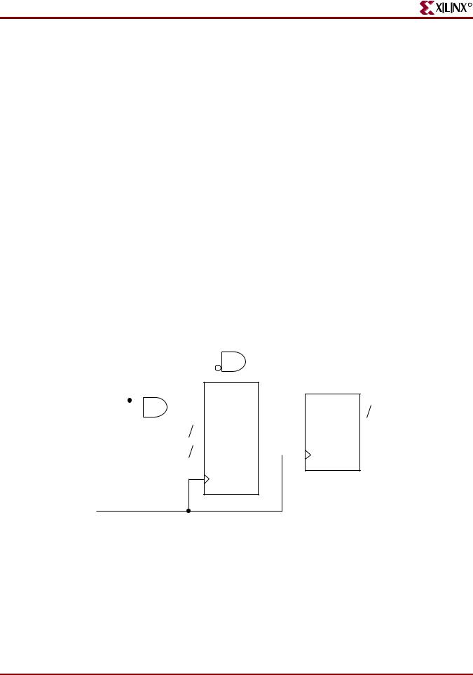
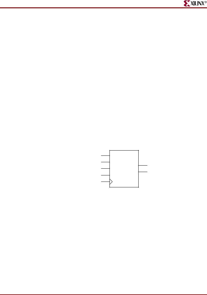
Single-Port RAM in Read-First Mode
This section discusses Single-Port RAM in Read-First Mode, and includes:
•“Single-Port RAM in Read-First Mode Diagram”
•“Single-Port RAM in Read-First Mode Pin Descriptions”
•“Single-Port RAM in Read-First Mode VHDL Coding Example”
•“Single-Port RAM in Read-First Mode Verilog Coding Example”
EN |
|
|
|
|
BRAM |
4 |
|
||||
|
|
|
|
WEA |
DOA |
|
DO |
||||
|
|
|
|
|
|||||||
WE |
|
|
|
|
|
|
|
|
|||
|
|
|
|
|
|
|
|||||
|
|
|
|
|
|
|
|
||||
|
|
|
|
|
|
|
|
|
|
||
4 |
|
|
|
|
|||||||
|
|
|
|
|
|
|
|||||
|
|
|
|
|
|
|
|
||||
DI |
|
|
|
|
DIA |
|
|
|
CE |
||
5 |
|
|
|
||||||||
|
|
|
|
|
|
|
|
||||
ADDR |
|
|
|
|
ADDRA |
|
|
|
|
|
|
|
|
|
|
|
|
|
|
|
|
||
|
CLK |
|
|
|
|
X10563 |
|
|
|
|
|
||
|
Figure 2-53: Single-Port RAM in Read-First Mode Diagram |
|||||
Table 2-67: |
Single-Port RAM in Read-First Mode Pin Descriptions |
|
||||
|
|
|
|
|
|
|
IO Pins |
|
Description |
|
|||
|
|
|
|
|
|
|
clk |
|
Positive-Edge Clock |
|
|||
|
|
|
|
|
|
|
we |
|
Synchronous Write Enable (Active High) |
|
|||
|
|
|
|
|
|
|
en |
|
Clock Enable |
|
|||
|
|
|
|
|
|
|
addr |
|
Read/Write Address |
|
|||
|
|
|
|
|
|
|
di |
|
Data Input |
|
|||
|
|
|
|
|
|
|
do |
|
Data Output |
|
|||
|
|
|
|
|
|
|
Single-Port RAM in Read-First Mode VHDL Coding Example
--
-- Read-First Mode
--
library ieee;
use ieee.std_logic_1164.all; use ieee.std_logic_unsigned.all;
entity rams_01 |
is |
port (clk |
: in std_logic; |
we |
: in std_logic; |
en |
: in std_logic; |
addr |
: in std_logic_vector(5 downto 0); |
di |
: in std_logic_vector(15 downto 0); |
XST User Guide |
www.xilinx.com |
165 |
10.1

Chapter 2: XST HDL Coding Techniques
R
do : out std_logic_vector(15 downto 0)); end rams_01;
architecture syn of rams_01 is
type ram_type is array (63 downto 0) of std_logic_vector (15 downto
0);
signal RAM: ram_type; begin
process (clk) begin
if clk'event and clk = '1' then if en = '1' then
if we = '1' then RAM(conv_integer(addr)) <= di;
end if;
do <= RAM(conv_integer(addr)) ; end if;
end if; end process;
end syn;
Single-Port RAM in Read-First Mode Verilog Coding Example
//
// Read-First Mode
//
module v_rams_01 (clk, en, we, addr, di, do);
input |
clk; |
input |
we; |
input |
en; |
input |
[5:0] addr; |
input |
[15:0] di; |
output |
[15:0] do; |
reg |
[15:0] RAM [63:0]; |
reg |
[15:0] do; |
always @(posedge clk) begin
if (en) begin
if (we) RAM[addr]<=di;
do <= RAM[addr];
end
end
endmodule
166 |
www.xilinx.com |
XST User Guide |
|
|
10.1 |
R
RAMs and ROMs HDL Coding Techniques
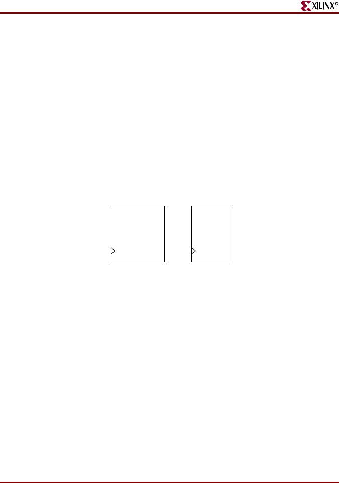
Single-Port RAM in Write-First Mode
This section discusses Single-Port RAM In Write-First Mode, and includes:
•“Single-Port RAM in Write-First Mode Diagram”
•“Single-Port RAM in Write-First Mode Pin Descriptions”
•“Single-Port RAM in Write-First Mode VHDL Coding Example One”
•“Single-Port RAM in Write-First Mode VHDL Coding Example Two”
•“Single-Port RAM In Write-First Mode Verilog Coding Example One”
•“Single-Port RAM In Write-First Mode Verilog Coding Example Two”
|
BRAM |
|
4 |
|
EN |
WEA |
DOA |
MUX |
|
WE |
DO |
|||
4 |
|
|
|
|
|
|
|
|
|
DI |
DIA |
|
|
|
|
5 |
|
|
CE |
ADDR |
ADDRA |
|
|
|
|
|
|
||
CLK |
|
|
|
X10564 |
Figure 2-54: Single-Port RAM in Write-First Mode Diagram
Table 2-68: Single-Port RAM in Write-First Mode Pin Descriptions
IO Pins |
Description |
|
|
clk |
Positive-Edge Clock |
|
|
we |
Synchronous Write Enable (Active High) |
|
|
en |
Clock Enable |
|
|
addr |
Read/Write Address |
|
|
di |
Data Input |
|
|
do |
Data Output |
|
|
Single-Port RAM in Write-First Mode VHDL Coding Example One
--
-- Write-First Mode (template 1)
--
library ieee;
use ieee.std_logic_1164.all; use ieee.std_logic_unsigned.all;
entity rams_02a is
port (clk |
: |
in |
std_logic; |
we |
: |
in |
std_logic; |
XST User Guide |
www.xilinx.com |
167 |
10.1

Chapter 2: XST HDL Coding Techniques
R
en |
: in std_logic; |
addr |
: in std_logic_vector(5 downto 0); |
di |
: in std_logic_vector(15 downto 0); |
do |
: out std_logic_vector(15 downto 0)); |
end rams_02a; |
|
architecture syn of rams_02a is
type ram_type is array (63 downto 0) of std_logic_vector (15 downto 0);
signal RAM : ram_type; begin
process (clk) begin
if clk'event and clk = '1' then if en = '1' then
if we = '1' then RAM(conv_integer(addr)) <= di; do <= di;
else
do <= RAM( conv_integer(addr)); end if;
end if; end if;
end process;
end syn;
Single-Port RAM in Write-First Mode VHDL Coding Example Two
--
-- Write-First Mode (template 2)
--
library ieee;
use ieee.std_logic_1164.all; use ieee.std_logic_unsigned.all;
entity rams_02b is
port (clk |
: in std_logic; |
we |
: in std_logic; |
en |
: in std_logic; |
addr |
: in std_logic_vector(5 downto 0); |
di |
: in std_logic_vector(15 downto 0); |
do |
: out std_logic_vector(15 downto 0)); |
end rams_02b;
architecture syn of rams_02b is
type ram_type is array (63 downto 0) of std_logic_vector (15 downto
0);
signal RAM : ram_type;
signal read_addr: std_logic_vector(5 downto 0); begin
process (clk) begin
if clk'event and clk = '1' then if en = '1' then
168 |
www.xilinx.com |
XST User Guide |
|
|
10.1 |

R
RAMs and ROMs HDL Coding Techniques
if we = '1' then ram(conv_integer(addr)) <= di;
end if;
read_addr <= addr; end if;
end if; end process;
do <= ram(conv_integer(read_addr));
end syn;
Single-Port RAM In Write-First Mode Verilog Coding Example One
//
// Write-First Mode (template 1)
//
module v_rams_02a (clk, we, en, addr, di, do);
input |
clk; |
input |
we; |
input |
en; |
input |
[5:0] addr; |
input |
[15:0] di; |
output |
[15:0] do; |
reg |
[15:0] RAM [63:0]; |
reg |
[15:0] do; |
always @(posedge clk) begin
if (en) begin
if (we) begin
RAM[addr] <= di; do <= di;
end else
do <= RAM[addr];
end
end endmodule
Single-Port RAM In Write-First Mode Verilog Coding Example Two
//
// Write-First Mode (template 2)
//
module v_rams_02b (clk, we, en, addr, di, do);
input clk; input we; input en;
input [5:0] addr; input [15:0] di;
XST User Guide |
www.xilinx.com |
169 |
10.1
Chapter 2: XST HDL Coding Techniques
R
output |
[15:0] do; |
reg |
[15:0] RAM [63:0]; |
reg |
[5:0] read_addr; |
always |
@(posedge clk) |
begin |
|
if |
(en) |
begin
if (we)
RAM[addr] <= di; read_addr <= addr;
end
end
assign do = RAM[read_addr];
endmodule
Single-Port RAM In No-Change Mode
This section discusses Single-Port RAM In No-Change Mode, and includes:
•“Single-Port RAM In No-Change Mode Diagram”
•“Single-Port RAM In No-Change Mode Pin Descriptions”
•“Single-Port RAM In No-Change Mode VHDL Coding Example”
•“Single-Port RAM In No-Change Mode Verilog Coding Example”
|
|
|
|
|
|
|
|
|
|
|
|
|
|
|
|
|
|
|
|
|
|
|
|
|
|
|
|
|
|
|
|
|
|
BRAM |
4 |
|
|||||
EN |
|
|
|
|
|
WEA DOA |
|
DO |
|||||
|
|
|
|
|
|
||||||||
WE |
|
|
|
|
|
|
|
|
|
||||
|
|
|
|
|
|
|
|
||||||
|
|
|
|
|
|
|
|
|
|||||
|
|
|
|
|
|
|
|
|
|
|
|
||
4 |
|
|
|
|
|
||||||||
|
|
|
|
|
|
|
|
||||||
|
|
|
|
|
|
|
|
|
|||||
DI |
|
|
|
|
|
DIA |
|
|
|
|
|||
5 |
|
CE |
|||||||||||
|
|
|
|
|
|
||||||||
ADDR |
|
|
|
|
|
ADDRA |
|
||||||
|
|
|
|
|
|
|
|
|
|||||
X10565
CLK
Figure 2-55: Single-Port RAM In No-Change Mode Diagram
Table 2-69: Single-Port RAM In No-Change Mode Pin Descriptions
IO Pins |
Description |
|
|
clk |
Positive-Edge Clock |
|
|
we |
Synchronous Write Enable (Active High) |
|
|
en |
Clock Enable |
|
|
170 |
www.xilinx.com |
XST User Guide |
|
|
10.1 |
R
RAMs and ROMs HDL Coding Techniques
Table 2-69: |
Single-Port RAM In No-Change Mode Pin Descriptions (Cont’d) |
|
|
|
|
IO Pins |
|
Description |
|
|
|
addr |
|
Read/Write Address |
|
|
|
di |
|
Data Input |
|
|
|
do |
|
Data Output |
|
|
|
Single-Port RAM In No-Change Mode VHDL Coding Example
--
-- No-Change Mode (template 1)
--
library ieee;
use ieee.std_logic_1164.all; use ieee.std_logic_unsigned.all;
entity rams_03 |
is |
port (clk |
: in std_logic; |
we |
: in std_logic; |
en |
: in std_logic; |
addr |
: in std_logic_vector(5 downto 0); |
di |
: in std_logic_vector(15 downto 0); |
do |
: out std_logic_vector(15 downto 0)); |
end rams_03; |
|
architecture syn of rams_03 is
type ram_type is array (63 downto 0) of std_logic_vector (15 downto
0);
signal RAM : ram_type; begin
process (clk) begin
if clk'event and clk = '1' then if en = '1' then
if we = '1' then RAM(conv_integer(addr)) <= di;
else
do <= RAM( conv_integer(addr)); end if;
end if; end if;
end process;
end syn;
Single-Port RAM In No-Change Mode Verilog Coding Example
//
// No-Change Mode (template 1)
//
module v_rams_03 (clk, we, en, addr, di, do);
input clk; input we;
XST User Guide |
www.xilinx.com |
171 |
10.1

Chapter 2: XST HDL Coding Techniques
R
input |
en; |
input |
[5:0] addr; |
input |
[15:0] di; |
output |
[15:0] do; |
reg |
[15:0] RAM [63:0]; |
reg |
[15:0] do; |
always |
@(posedge clk) |
begin |
|
if |
(en) |
begin
if (we)
RAM[addr] <= di; else
do <= RAM[addr];
end
end
endmodule
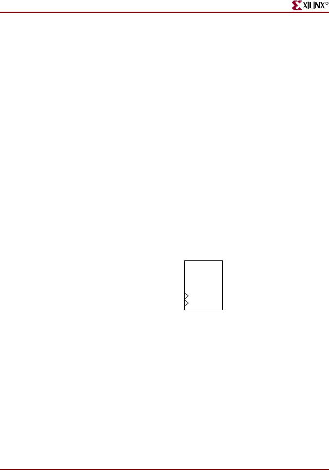
Single-Port RAM With Asynchronous Read
This section discusses Single-Port RAM With Asynchronous Read, and includes:
•“Single-Port RAM With Asynchronous Read Diagram”
•“Single-Port RAM With Asynchronous Read Pin Descriptions”
•“Single-Port RAM With Asynchronous Read VHDL Coding Example”
•“Single-Port RAM With Asynchronous Read Verilog Coding Example”
The following descriptions are directly mappable onto distributed RAM only.
|
WE |
|
|
|
|
|
|
|
|
|
|
||
|
|
DI |
|
Distributed |
|
DO |
|
|
|
|
|||
|
|
A |
|
RAM |
|
|
|
|
|
|
|
||
|
|
|
|
|
||
|
CLK |
|
|
X8976 |
||
|
|
|
||||
|
|
|
|
|
||
|
|
|
|
|
||
|
Figure 2-56: Single-Port RAM With Asynchronous Read Diagram |
|||||
Table 2-70: |
Single-Port RAM With Asynchronous Read Pin Descriptions |
|||||
|
|
|
|
|
|
|
IO Pins |
|
Description |
|
|
||
|
|
|
|
|
|
|
clk |
|
Positive-Edge Clock |
|
|
||
|
|
|
|
|
|
|
we |
|
Synchronous Write Enable (Active High) |
||||
|
|
|
|
|
|
|
a |
|
Read/Write Address |
|
|
||
|
|
|
|
|
|
|
di |
|
Data Input |
|
|
||
|
|
|
|
|
|
|
do |
|
Data Output |
|
|
||
|
|
|
|
|
|
|
172 |
www.xilinx.com |
XST User Guide |
|
|
10.1 |

R
RAMs and ROMs HDL Coding Techniques
Single-Port RAM With Asynchronous Read VHDL Coding Example
--
-- Single-Port RAM with Asynchronous Read
--
library ieee;
use ieee.std_logic_1164.all; use ieee.std_logic_unsigned.all;
entity rams_04 is
port (clk : in std_logic; we : in std_logic;
a : in std_logic_vector(5 downto 0); di : in std_logic_vector(15 downto 0); do : out std_logic_vector(15 downto 0));
end rams_04;
architecture syn of rams_04 is
type ram_type is array (63 downto 0) of std_logic_vector (15 downto
0);
signal RAM : ram_type; begin
process (clk) begin
if (clk'event and clk = '1') then if (we = '1') then
RAM(conv_integer(a)) <= di; end if;
end if; end process;
do <= RAM(conv_integer(a));
end syn;
Single-Port RAM With Asynchronous Read Verilog Coding Example
//
// Single-Port RAM with Asynchronous Read
//
module v_rams_04 (clk, we, a, di, do);
input |
clk; |
input |
we; |
input |
[5:0] a; |
input |
[15:0] di; |
output |
[15:0] do; |
reg |
[15:0] ram [63:0]; |
always |
@(posedge clk) begin |
if |
(we) |
|
ram[a] <= di; |
end |
|
assign |
do = ram[a]; |
endmodule |
|
XST User Guide |
www.xilinx.com |
173 |
10.1

Chapter 2: XST HDL Coding Techniques
R
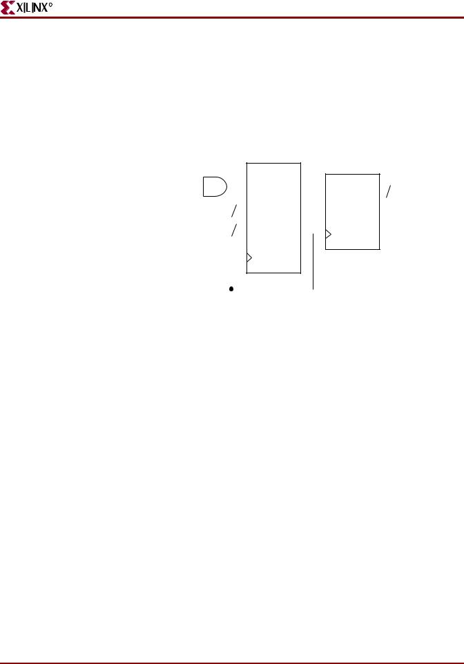
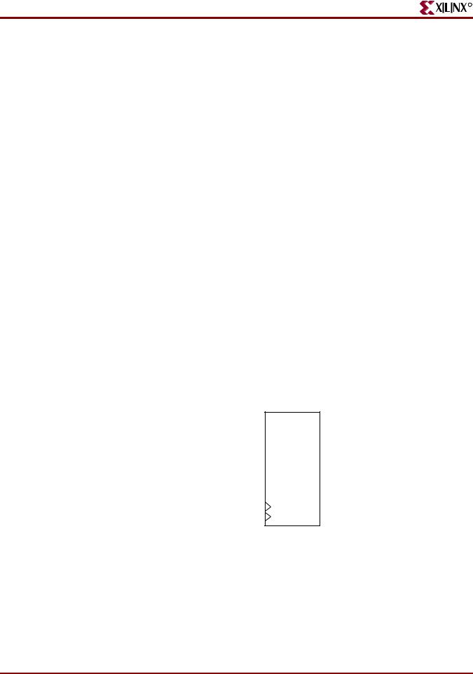
Single-Port RAM With False Synchronous Read
This section discusses Single-Port RAM With False Synchronous Read, and includes:
•“Single-Port RAM With False Synchronous Read Diagram”
•“Single-Port RAM With False Synchronous Read Pin Descriptions”
•“Single-Port RAM With False Synchronous Read VHDL Coding Example”
•“Single-Port RAM With False Synchronous Read Verilog Coding Example”
The following descriptions do not implement true synchronous read access as defined by the Virtex block RAM specification, where the read address is registered. They are mappable only onto distributed RAM with an additional buffer on the data output for the Virtex and Virtex-E families, as shown in Figure 2-57, “Single-Port RAM With False Synchronous Read Diagram.” For Virtex-II devices and higher, this code is mappable on block RAM.
WE |
|
|
|
|
|
|
|
|
|
|
|
|
|
|
|
|
|
|
|
DI |
|
|
|
Distributed |
|
|
D |
|
DO |
|
|
|
|
|
|
||||
A |
|
|
|
RAM |
|
|
|
||
|
|
|
|
|
|
|
|
||
|
|
|
|
|
|
|
|
||
CLK |
|
|
|
|
|
|
|
|
X8977 |
|
|
|
|
|
|
|
|
||
|
|
|
|
|
|
|
|
|
|
|
|
|
|
|
|
|
|
|
|
|
|
|
|
|
|
|
|
|
|
Figure 2-57: Single-Port RAM With False Synchronous Read Diagram |
|||||||||
Table 2-71: Single-Port RAM With False Synchronous Read Pin Descriptions |
|||||||||
|
|
|
|
|
|
|
|
|
|
IO Pins |
Description |
|
|
||||||
|
|
|
|
|
|
|
|
|
|
clk |
Positive-Edge Clock |
|
|
||||||
|
|
|
|
|
|
|
|
|
|
we |
Synchronous Write Enable (Active High) |
||||||||
|
|
|
|
|
|
|
|
|
|
a |
Read/Write Address |
|
|
||||||
|
|
|
|
|
|
|
|
|
|
di |
Data Input |
|
|
||||||
|
|
|
|
|
|
|
|
|
|
do |
Data Output |
|
|
||||||
|
|
|
|
|
|
|
|
|
|
Single-Port RAM With False Synchronous Read VHDL Coding Example
--
-- Single-Port RAM with "False" Synchronous Read
--
library ieee;
use ieee.std_logic_1164.all; use ieee.std_logic_unsigned.all;
entity rams_05 is
port (clk : in std_logic; we : in std_logic;
174 |
www.xilinx.com |
XST User Guide |
|
|
10.1 |

R
RAMs and ROMs HDL Coding Techniques
a : in std_logic_vector(5 downto 0); di : in std_logic_vector(15 downto 0); do : out std_logic_vector(15 downto 0));
end rams_05;
architecture syn of rams_05 is
type ram_type is array (63 downto 0) of std_logic_vector (15 downto 0);
signal RAM : ram_type; begin
process (clk) begin
if (clk'event and clk = '1') then if (we = '1') then
RAM(conv_integer(a)) <= di; end if;
do <= RAM(conv_integer(a)); end if;
end process;
end syn;
Single-Port RAM With False Synchronous Read Verilog Coding Example
//
// Single-Port RAM with "False" Synchronous Read
//
module v_rams_05 (clk, we, a, di, do);
input |
clk; |
|
input |
we; |
|
input |
[5:0] a; |
|
input |
[15:0] di; |
|
output |
[15:0] do; |
|
reg |
[15:0] ram |
[63:0]; |
reg |
[15:0] do; |
|
always |
@(posedge clk) begin |
|
if |
(we) |
|
|
ram[a] <= |
di; |
do |
<= ram[a]; |
|
end |
|
|
endmodule
XST User Guide |
www.xilinx.com |
175 |
10.1
Chapter 2: XST HDL Coding Techniques
R
Single-Port RAM With False Synchronous Read and Reset on the Output
This section discusses Single-Port RAM With False Synchronous Read and Reset on the Output, and includes:
•“Single-Port RAM With False Synchronous Read and Reset on the Output Diagram”
•“Single-Port RAM With False Synchronous Read and Reset on the Output Pin Descriptions”
•“Single-Port RAM With False Synchronous Read and Reset on the Output VHDL Coding Example”
•“Single-Port RAM With False Synchronous Read and Reset on the Output Verilog Coding Example”
The following descriptions, featuring an additional reset of the RAM output, are also only mappable onto Distributed RAM with an additional resetable buffer on the data output as shown in Figure 2-58, “Single-Port RAM With False Synchronous Read and Reset on the Output Diagram.”
WE |
|
|
|
RST |
|
|
||||
|
|
|
|
|
|
DO |
||||
|
|
|
|
|
|
|
|
|
||
|
|
|
|
|
|
|
|
|
||
|
|
|
|
|
|
|
|
|
||
DI |
|
|
Distributed |
|
|
|
D |
|||
|
|
|
|
|
||||||
A |
|
|
RAM |
|
|
|
|
|
|
|
|
|
|
|
|
|
|
|
|
|
|
CLK |
|
|
|
|
|
|
|
|
X10566 |
|
|
|
|
|
|
|
|
|
|||
|
|
|
|
|
|
|
|
|
||
|
|
|
|
|
|
|
||||
Figure 2-58: Single-Port RAM With False Synchronous Read and Reset on the Output Diagram
Table 2-72: Single-Port RAM With False Synchronous Read and Reset on the Output Pin Descriptions
IO Pins |
Description |
|
|
clk |
Positive-Edge Clock |
|
|
we |
Synchronous Write Enable (Active High) |
|
|
rst |
Synchronous Output Reset (Active High) |
|
|
a |
Read/Write Address |
|
|
di |
Data Input |
|
|
do |
Data Output |
|
|
Single-Port RAM With False Synchronous Read and Reset on the Output VHDL Coding Example
--Single-Port RAM with "False" Synchronous Read with
--an additional reset of the RAM output,
library ieee;
use ieee.std_logic_1164.all;
176 |
www.xilinx.com |
XST User Guide |
|
|
10.1 |

R
RAMs and ROMs HDL Coding Techniques
use ieee.std_logic_unsigned.all;
entity rams_06 is
port (clk : in std_logic; we : in std_logic; rst : in std_logic;
a : in std_logic_vector(5 downto 0); di : in std_logic_vector(15 downto 0); do : out std_logic_vector(15 downto 0));
end rams_06;
architecture syn of rams_06 is
type ram_type is array (63 downto 0) of std_logic_vector (15 downto
0);
signal RAM : ram_type; begin
process (clk) begin
if (clk'event and clk = '1') then
if (we = '1') then RAM(conv_integer(a)) <= di;
end if;
if (rst = '1') then
do <= (others => '0');
else
do <= RAM(conv_integer(a)); end if;
end if; end process;
end syn;
Single-Port RAM With False Synchronous Read and Reset on the Output Verilog Coding Example
//
//Single-Port RAM with "False" Synchronous Read with
//an additional reset of the RAM output,
//
module v_rams_06 (clk, we, rst, a, di, do);
input |
clk; |
input |
we; |
input |
rst; |
input |
[5:0] a; |
input |
[15:0] di; |
output |
[15:0] do; |
reg |
[15:0] ram [63:0]; |
reg |
[15:0] do; |
always |
@(posedge clk) begin |
if |
(we) |
|
ram[a] <= di; |
XST User Guide |
www.xilinx.com |
177 |
10.1
Chapter 2: XST HDL Coding Techniques
R
if (rst)
do <= 16'h0000; else
do <= ram[a];
end
endmodule
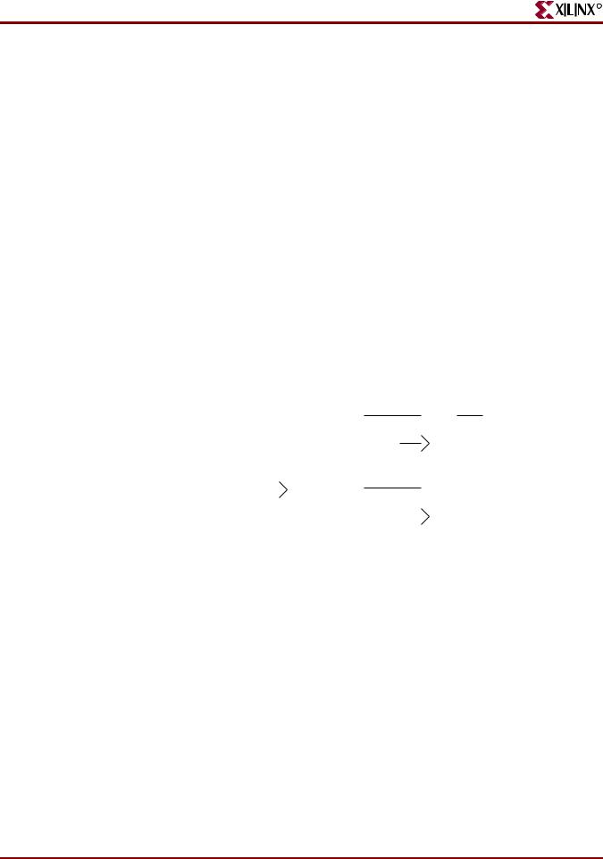
Single-Port RAM With Synchronous Read (Read Through)
This section discusses Single-Port RAM With Synchronous Read (Read Through), and includes:
•“Single-Port RAM With Synchronous Read (Read Through) Diagram”
•“Single-Port RAM With Synchronous Read (Read Through) Pin Descriptions”
•“Single-Port RAM With Synchronous Read (Read Through) VHDL Coding Example”
•“Single-Port RAM With Synchronous Read (Read Through) Verilog Coding Example”
The following description implements a true synchronous read. A true synchronous read is the synchronization mechanism in Virtex block RAMs, where the read address is registered on the RAM clock edge. Such descriptions are directly mappable onto block RAM, as shown in Figure 2-59, “Single-Port RAM With Synchronous Read (Read Through) Diagram.” The same descriptions can also be mapped onto Distributed RAM.
.
WE
DI Block
DO
A RAM
CLK
X8979
Figure 2-59: Single-Port RAM With Synchronous Read (Read Through) Diagram
Table 2-73: Single-Port RAM With Synchronous Read (Read Through) Pin Descriptions
IO Pins |
Description |
|
|
clk |
Positive-Edge Clock |
|
|
we |
Synchronous Write Enable (Active High) |
|
|
a |
Read/Write Address |
|
|
di |
Data Input |
|
|
do |
Data Output |
|
|
178 |
www.xilinx.com |
XST User Guide |
|
|
10.1 |

R
RAMs and ROMs HDL Coding Techniques
Single-Port RAM With Synchronous Read (Read Through) VHDL Coding Example
--
-- Single-Port RAM with Synchronous Read (Read Through)
--
library ieee;
use ieee.std_logic_1164.all; use ieee.std_logic_unsigned.all;
entity rams_07 is
port (clk : in std_logic; we : in std_logic;
a : in std_logic_vector(5 downto 0); di : in std_logic_vector(15 downto 0); do : out std_logic_vector(15 downto 0));
end rams_07;
architecture syn of rams_07 is
type ram_type is array (63 downto 0) of std_logic_vector (15 downto
0);
signal RAM : ram_type;
signal read_a : std_logic_vector(5 downto 0); begin
process (clk) begin
if (clk'event and clk = '1') then if (we = '1') then
RAM(conv_integer(a)) <= di; end if;
read_a <= a; end if;
end process;
do <= RAM(conv_integer(read_a));
end syn;
Single-Port RAM With Synchronous Read (Read Through) Verilog Coding Example
//
// Single-Port RAM with Synchronous Read (Read Through)
//
module v_rams_07 (clk, we, a, di, do);
input |
clk; |
input |
we; |
input |
[5:0] a; |
input |
[15:0] di; |
output |
[15:0] do; |
reg |
[15:0] ram [63:0]; |
reg |
[5:0] read_a; |
always |
@(posedge clk) begin |
if |
(we) |
|
ram[a] <= di; |
read_a <= a;
XST User Guide |
www.xilinx.com |
179 |
10.1

Chapter 2: XST HDL Coding Techniques
R
end
assign do = ram[read_a];
endmodule
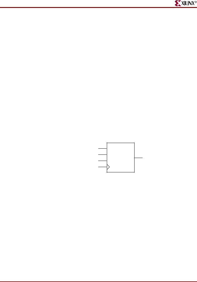
Single-Port RAM With Enable
This section discusses Single-Port RAM With Enable, and includes:
•“Single-Port RAM With Enable Diagram”
•“Single-Port RAM With Enable Pin Descriptions”
•“Single-Port RAM With Enable VHDL Coding Example”
•“Single-Port RAM With Enable Verilog Coding Example”
|
A |
|
|
|
|
|
DO |
|
|
|
|
|
|
|
|||
|
EN |
|
|
Block |
|
|
||
|
|
|
|
|||||
|
WE |
|
|
|
|
|||
|
|
|
|
|
||||
|
DI |
|
|
RAM |
|
|
||
|
|
|
|
|
|
|
||
|
CLK |
|
|
|
|
X9478 |
||
|
|
|
|
|
||||
|
|
|
|
|
|
|
||
|
|
|
|
|
|
|
||
|
Figure 2-60: Single-Port RAM With Enable Diagram |
|||||||
Table 2-74: |
Single-Port RAM With Enable |
Pin Descriptions |
||||||
|
|
|
|
|
|
|
|
|
IO Pins |
|
Description |
|
|
|
|||
|
|
|
|
|
|
|
||
clk |
|
Positive-Edge Clock |
||||||
|
|
|
|
|
|
|
|
|
en |
|
Global Enable |
|
|
|
|||
|
|
|
|
|
|
|
||
we |
|
Synchronous Write Enable (Active High) |
||||||
|
|
|
|
|
|
|
||
a |
|
Read/Write Address |
||||||
|
|
|
|
|
|
|
|
|
di |
|
Data Input |
|
|
|
|
||
|
|
|
|
|
|
|
|
|
do |
|
Data Output |
|
|
|
|||
|
|
|
|
|
|
|
|
|
180 |
www.xilinx.com |
XST User Guide |
|
|
10.1 |
R
RAMs and ROMs HDL Coding Techniques
Single-Port RAM With Enable VHDL Coding Example
--
-- Single-Port RAM with Enable
--
library ieee;
use ieee.std_logic_1164.all; use ieee.std_logic_unsigned.all;
entity rams_08 is
port (clk : in std_logic; en : in std_logic; we : in std_logic;
a : in std_logic_vector(5 downto 0); di : in std_logic_vector(15 downto 0); do : out std_logic_vector(15 downto 0));
end rams_08;
architecture syn of rams_08 is
type ram_type is array (63 downto 0) of std_logic_vector (15 downto
0);
signal RAM : ram_type;
signal read_a : std_logic_vector(5 downto 0); begin
process (clk) begin
if (clk'event and clk = '1') then if (en = '1') then
if (we = '1') then RAM(conv_integer(a)) <= di;
end if; read_a <= a;
end if; end if;
end process;
do <= RAM(conv_integer(read_a));
end syn;
Single-Port RAM With Enable Verilog Coding Example
//
// Single-Port RAM with Enable
//
module v_rams_08 (clk, en, we, a, di, do);
input |
clk; |
input |
en; |
input |
we; |
input |
[5:0] a; |
input |
[15:0] di; |
output |
[15:0] do; |
reg |
[15:0] ram [63:0]; |
reg |
[5:0] read_a; |
XST User Guide |
www.xilinx.com |
181 |
10.1

Chapter 2: XST HDL Coding Techniques
R
always @(posedge clk) begin if (en)
begin
if (we)
ram[a] <= di; read_a <= a;
end
end
assign do = ram[read_a];
endmodule
Dual-Port RAM With Asynchronous Read
This section discusses Dual-Port RAM With Asynchronous Read, and includes:
•“Dual-Port RAM With Asynchronous Read Diagram”
•“Dual-Port RAM With Asynchronous Read Pin Descriptions”
•“Dual-Port RAM With Asynchronous Read VHDL Coding Example”
•“Dual-Port RAM With Asynchronous Read Verilog Coding Example”
Figure 2-61, “Dual-Port RAM With Asynchronous Read Diagram,” shows where the two output ports are used. It is directly mappable onto Distributed RAM only.
|
DPRA |
|
|
|
|
|
|
|
|
|
|
|
|
||
|
WE |
|
Distributed |
|
SPO |
||
|
|
|
|||||
|
|
DI |
|
|
|||
|
|
|
|
||||
|
|
|
|
RAM |
|
DPO |
|
|
|
A |
|
|
|
||
|
|
|
|
|
|||
|
|
|
|
|
|
|
|
|
|
|
|
|
|
|
|
|
CLK |
|
|
|
|
X8980 |
|
|
|
|
|
|
|||
|
|
|
|
|
|
|
|
|
|
|
|
|
|
|
|
|
Figure 2-61: Dual-Port RAM With Asynchronous Read Diagram |
||||||
Table 2-75: |
Dual-Port RAM With Asynchronous Read Pin Descriptions |
||||||
|
|
|
|
|
|
|
|
IO Pins |
|
Description |
|
|
|
||
|
|
|
|
|
|
|
|
clk |
|
Positive-Edge Clock |
|
|
|||
|
|
|
|
|
|
|
|
we |
|
Synchronous Write Enable (Active High) |
|||||
|
|
|
|
|
|
|
|
a |
|
Write Address/Primary Read Address |
|||||
|
|
|
|
|
|
|
|
dpra |
|
Dual Read Address |
|
|
|||
|
|
|
|
|
|
|
|
di |
|
Data Input |
|
|
|
||
|
|
|
|
|
|
|
|
spo |
|
Primary Output Port |
|
|
|||
|
|
|
|
|
|
|
|
dpo |
|
Dual Output Port |
|
|
|||
|
|
|
|
|
|
|
|
182 |
www.xilinx.com |
XST User Guide |
|
|
10.1 |

R
RAMs and ROMs HDL Coding Techniques
Dual-Port RAM With Asynchronous Read VHDL Coding Example
--
-- Dual-Port RAM with Asynchronous Read
--
library ieee;
use ieee.std_logic_1164.all; use ieee.std_logic_unsigned.all;
entity rams_09 |
is |
port (clk |
: in std_logic; |
we |
: in std_logic; |
a |
: in std_logic_vector(5 downto 0); |
dpra |
: in std_logic_vector(5 downto 0); |
di |
: in std_logic_vector(15 downto 0); |
spo |
: out std_logic_vector(15 downto 0); |
dpo |
: out std_logic_vector(15 downto 0)); |
end rams_09; |
|
architecture syn of rams_09 is
type ram_type is array (63 downto 0) of std_logic_vector (15 downto
0);
signal RAM : ram_type; begin
process (clk) begin
if (clk'event and clk = '1') then if (we = '1') then
RAM(conv_integer(a)) <= di; end if;
end if; end process;
spo <= RAM(conv_integer(a)); dpo <= RAM(conv_integer(dpra));
end syn;
Dual-Port RAM With Asynchronous Read Verilog Coding Example
//
// Dual-Port RAM with Asynchronous Read
//
module v_rams_09 (clk, we, a, dpra, di, spo, dpo);
input |
clk; |
input |
we; |
input |
[5:0] a; |
input |
[5:0] dpra; |
input |
[15:0] di; |
output |
[15:0] spo; |
output |
[15:0] dpo; |
reg |
[15:0] ram [63:0]; |
always |
@(posedge clk) begin |
if |
(we) |
XST User Guide |
www.xilinx.com |
183 |
10.1
Chapter 2: XST HDL Coding Techniques
R
ram[a] <= di;
end
assign spo = ram[a]; assign dpo = ram[dpra];
endmodule
Dual-Port RAM With False Synchronous Read
This section discusses Dual-Port RAM With False Synchronous Read, and includes:
•“Dual-Port RAM With False Synchronous Read Diagram”
•“Dual-Port RAM With False Synchronous Read Pin Descriptions”
•“Dual-Port RAM With False Synchronous Read VHDL Coding Example”
•“Dual-Port RAM With False Synchronous Read Verilog Coding Example”
The following description is mapped onto Distributed RAM with additional registers on the data outputs for Virtex and Virtex-E devices. For Virtex-II devices and higher, this code is mappable on block RAM.
DPRA |
|
|
|
|
|
D |
|
SPO |
|
|
|
|
|
|
|||
|
|
|
||||||
WE |
|
|
Distributed |
CLK |
|
|
|
|
|
|
|
|
|
||||
DI |
|
|
|
|
|
|||
|
|
RAM |
|
|
|
|
|
|
|
|
|
|
|
|
|
||
A |
|
|
|
|
D |
|
DPO |
|
|
|
|
|
|
|
|||
|
|
|
|
|
|
|||
CLK |
|
|
|
CLK |
|
|
||
|
|
|
|
|
||||
|
|
|
||||||
|
|
|
|
|
|
|
X8981 |
|
|
|
|
|
|
|
|
||
|
|
|
|
|
|
|
||
|
|
|
|
|
|
|
|
|
|
|
|
|
|
|
|
|
|
Figure 2-62: Dual-Port RAM With False Synchronous Read Diagram |
||||||||
Table 2-76: Dual-Port RAM With False Synchronous Read Pin Descriptions |
||||||||
|
|
|
|
|
|
|
|
|
IO Pins |
Description |
|
|
|
|
|
||
|
|
|
|
|
|
|
|
|
clk |
Positive-Edge Clock |
|
|
|||||
|
|
|
|
|
|
|
|
|
we |
Synchronous Write Enable (Active High) |
|||||||
|
|
|
|
|
|
|
|
|
a |
Write Address/Primary Read Address |
|||||||
|
|
|
|
|
|
|
|
|
dpra |
Dual Read Address |
|
|
|||||
|
|
|
|
|
|
|
|
|
di |
Data Input |
|
|
|
|
|
||
|
|
|
|
|
|
|
|
|
spo |
Primary Output Port |
|
|
|||||
|
|
|
|
|
|
|
|
|
dpo |
Dual Output Port |
|
|
|||||
|
|
|
|
|
|
|
|
|
184 |
www.xilinx.com |
XST User Guide |
|
|
10.1 |

R
RAMs and ROMs HDL Coding Techniques
Dual-Port RAM With False Synchronous Read VHDL Coding Example
--
-- Dual-Port RAM with False Synchronous Read
--
library ieee;
use ieee.std_logic_1164.all; use ieee.std_logic_unsigned.all;
entity rams_10 |
is |
port (clk |
: in std_logic; |
we |
: in std_logic; |
a |
: in std_logic_vector(5 downto 0); |
dpra |
: in std_logic_vector(5 downto 0); |
di |
: in std_logic_vector(15 downto 0); |
spo |
: out std_logic_vector(15 downto 0); |
dpo |
: out std_logic_vector(15 downto 0)); |
end rams_10; |
|
architecture syn of rams_10 is
type ram_type is array (63 downto 0) of std_logic_vector (15 downto
0);
signal RAM : ram_type; begin
process (clk) begin
if (clk'event and clk = '1') then if (we = '1') then
RAM(conv_integer(a)) <= di; end if;
spo <= RAM(conv_integer(a)); dpo <= RAM(conv_integer(dpra));
end if; end process;
end syn;
Dual-Port RAM With False Synchronous Read Verilog Coding Example
//
// Dual-Port RAM with False Synchronous Read
//
module v_rams_10 (clk, we, a, dpra, di, spo, dpo);
input |
clk; |
input |
we; |
input |
[5:0] a; |
input |
[5:0] dpra; |
input |
[15:0] di; |
output |
[15:0] spo; |
output |
[15:0] dpo; |
reg |
[15:0] ram [63:0]; |
reg |
[15:0] spo; |
reg |
[15:0] dpo; |
XST User Guide |
www.xilinx.com |
185 |
10.1
Chapter 2: XST HDL Coding Techniques
R
always @(posedge clk) begin if (we)
ram[a] <= di;
spo <= ram[a]; dpo <= ram[dpra];
end
endmodule
Dual-Port RAM With Synchronous Read (Read Through)
This section discusses Dual-Port RAM With Synchronous Read (Read Through), and includes:
•“Dual-Port RAM With Synchronous Read (Read Through) Diagram”
•“Dual-Port RAM With Synchronous Read (Read Through) Pin Descriptions”
•“Dual-Port RAM With Synchronous Read (Read Through) VHDL Coding Example”
•“Dual-Port RAM With Synchronous Read (Read Through) Verilog Coding Example”
The following descriptions are directly mappable onto block RAM, as shown in
Figure 2-63, “Dual-Port RAM With Synchronous Read (Read Through) Diagram.” They may also be implemented with Distributed RAM.
DPRA
WE
Block SPO
DI
RAM DPO
A
CLK
X8982
Figure 2-63: Dual-Port RAM With Synchronous Read (Read Through) Diagram
Table 2-77: Dual-Port RAM With Synchronous Read (Read Through) Pin Descriptions
IO Pins |
Description |
|
|
clk |
Positive-Edge Clock |
|
|
we |
Synchronous Write Enable (Active High) |
|
|
a |
Write Address/Primary Read Address |
|
|
dpra |
Dual Read Address |
|
|
di |
Data Input |
|
|
spo |
Primary Output Port |
|
|
dpo |
Dual Output Port |
|
|
186 |
www.xilinx.com |
XST User Guide |
|
|
10.1 |

R
RAMs and ROMs HDL Coding Techniques
Dual-Port RAM With Synchronous Read (Read Through) VHDL Coding Example
--
-- Dual-Port RAM with Synchronous Read (Read Through)
--
library ieee;
use ieee.std_logic_1164.all; use ieee.std_logic_unsigned.all;
entity rams_11 |
is |
port (clk |
: in std_logic; |
we |
: in std_logic; |
a |
: in std_logic_vector(5 downto 0); |
dpra |
: in std_logic_vector(5 downto 0); |
di |
: in std_logic_vector(15 downto 0); |
spo |
: out std_logic_vector(15 downto 0); |
dpo |
: out std_logic_vector(15 downto 0)); |
end rams_11; |
|
architecture syn of rams_11 is
type ram_type is array (63 downto 0) of std_logic_vector (15 downto 0);
signal RAM : ram_type;
signal read_a : std_logic_vector(5 downto 0); signal read_dpra : std_logic_vector(5 downto 0);
begin
process (clk) begin
if (clk'event and clk = '1') then if (we = '1') then
RAM(conv_integer(a)) <= di; end if;
read_a <= a; read_dpra <= dpra;
end if; end process;
spo <= RAM(conv_integer(read_a)); dpo <= RAM(conv_integer(read_dpra));
end syn;
Dual-Port RAM With Synchronous Read (Read Through) Verilog Coding Example
//
// Dual-Port RAM with Synchronous Read (Read Through)
//
module v_rams_11 (clk, we, a, dpra, di, spo, dpo);
input clk; input we; input [5:0] a;
input [5:0] dpra; input [15:0] di; output [15:0] spo; output [15:0] dpo;
XST User Guide |
www.xilinx.com |
187 |
10.1
Chapter 2: XST HDL Coding Techniques
R
reg |
[15:0] ram [63:0]; |
reg |
[5:0] read_a; |
reg |
[5:0] read_dpra; |
always |
@(posedge clk) begin |
if |
(we) |
|
ram[a] <= di; |
read_a <= a; read_dpra <= dpra;
end
assign spo = ram[read_a]; assign dpo = ram[read_dpra];
endmodule
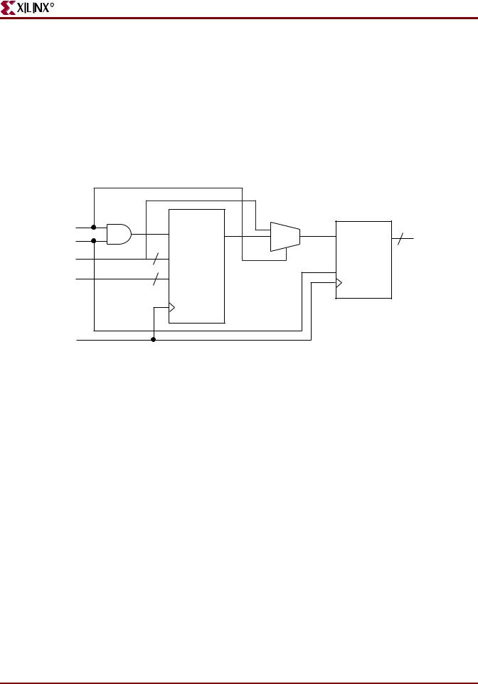
Dual-Port RAM With Synchronous Read (Read Through) and Two Clocks
This section discusses Dual-Port RAM With Synchronous Read (Read Through) and Two Clocks, and includes:
•“Dual-Port RAM With Synchronous Read (Read Through) and Two Clocks Diagram”
•“Dual-Port RAM With Synchronous Read (Read Through) and Two Clocks Pin Descriptions”
•“Dual-Port RAM With Synchronous Read (Read Through) and Two Clocks VHDL Coding Example”
•“Dual-Port RAM With Synchronous Read (Read Through) and Two Clocks Verilog Coding Example”
WE |
|
|
|
DO1 |
|
|
|
||
DI |
|
Block |
|
|
|
|
|||
ADD1 |
|
|
DO2 |
|
|
RAM |
|
||
ADD2 |
|
|
|
|
|
|
|
|
|
CLK1 |
|
|
|
|
|
|
|
|
|
CLK2 |
|
|
|
X10567 |
|
|
|
||
|
|
|
|
Figure 2-64: Dual-Port RAM With Synchronous Read (Read Through) and Two Clocks
Diagram
Table 2-78: Dual-Port RAM With Synchronous Read (Read Through) and Two Clocks Pin Descriptions
IO Pins |
Description |
|
|
clk1 |
Positive-Edge Write/Primary Read Clock |
|
|
clk2 |
Positive-Edge Dual Read Clock |
|
|
we |
Synchronous Write Enable (Active High) |
|
|
add1 |
Write/Primary Read Address |
|
|
add2 |
Dual Read Address |
|
|
di |
Data Input |
|
|
188 |
www.xilinx.com |
XST User Guide |
|
|
10.1 |

R
RAMs and ROMs HDL Coding Techniques
Table 2-78: Dual-Port RAM With Synchronous Read (Read Through) and Two Clocks (Cont’d) Pin Descriptions
IO Pins |
Description |
|
|
do1 |
Primary Output Port |
|
|
do2 |
Dual Output Port |
|
|
Dual-Port RAM With Synchronous Read (Read Through) and Two Clocks VHDL Coding Example
--
--Dual-Port RAM with Synchronous Read (Read Through)
--using More than One Clock
--
library ieee;
use ieee.std_logic_1164.all; use ieee.std_logic_unsigned.all;
entity rams_12 |
is |
port (clk1 |
: in std_logic; |
clk2 |
: in std_logic; |
we |
: in std_logic; |
add1 |
: in std_logic_vector(5 downto 0); |
add2 |
: in std_logic_vector(5 downto 0); |
di |
: in std_logic_vector(15 downto 0); |
do1 |
: out std_logic_vector(15 downto 0); |
do2 |
: out std_logic_vector(15 downto 0)); |
end rams_12; |
|
architecture syn of rams_12 is
type ram_type is array (63 downto 0) of std_logic_vector (15 downto
0);
signal RAM : ram_type;
signal read_add1 : std_logic_vector(5 downto 0); signal read_add2 : std_logic_vector(5 downto 0);
begin
process (clk1) begin
if (clk1'event and clk1 = '1') then if (we = '1') then
RAM(conv_integer(add1)) <= di; end if;
read_add1 <= add1; end if;
end process;
do1 <= RAM(conv_integer(read_add1));
process (clk2) begin
if (clk2'event and clk2 = '1') then read_add2 <= add2;
end if; end process;
XST User Guide |
www.xilinx.com |
189 |
10.1

Chapter 2: XST HDL Coding Techniques
R
do2 <= RAM(conv_integer(read_add2));
end syn;
Dual-Port RAM With Synchronous Read (Read Through) and Two Clocks Verilog Coding Example
//
//Dual-Port RAM with Synchronous Read (Read Through)
//using More than One Clock
//
module v_rams_12 (clk1, clk2, we, add1, add2, di, do1, do2);
input |
clk1; |
input |
clk2; |
input |
we; |
input |
[5:0] add1; |
input |
[5:0] add2; |
input |
[15:0] di; |
output |
[15:0] do1; |
output |
[15:0] do2; |
reg |
[15:0] ram [63:0]; |
reg |
[5:0] read_add1; |
reg |
[5:0] read_add2; |
always |
@(posedge clk1) begin |
if |
(we) |
|
ram[add1] <= di; |
read_add1 <= add1;
end
assign do1 = ram[read_add1];
always @(posedge clk2) begin read_add2 <= add2;
end
assign do2 = ram[read_add2];
endmodule
190 |
www.xilinx.com |
XST User Guide |
|
|
10.1 |
R
RAMs and ROMs HDL Coding Techniques
Dual-Port RAM With One Enable Controlling Both Ports
This section discusses Dual-Port RAM With One Enable Controlling Both Ports and includes:
•“Dual-Port RAM With One Enable Controlling Both Ports Diagram”
•“Dual-Port RAM With One Enable Controlling Both Ports Pin Descriptions”
•“Dual-Port RAM With One Enable Controlling Both Ports VHDL Coding Example”
•“Dual-Port RAM With One Enable Controlling Both Ports Verilog Coding Example”
ADDRA |
|
|
|
|
|
|
|
|
|
ADDRB |
|
|
DOA |
|
|
|
|||
EN |
|
Block |
|
|
|
|
|
||
WE |
|
RAM |
|
DOB |
|
|
|
||
DI |
|
|
|
|
|
|
|
|
|
CLK |
|
|
|
|
|
|
|
|
|
|
|
|
|
|
X10581
Figure 2-65: Dual-Port RAM With One Enable Controlling Both Ports Diagram
Table 2-79: Dual-Port RAM With One Enable Controlling Both Ports Pin Descriptions
IO Pins |
Description |
|
|
clk |
Positive-Edge Clock |
|
|
en |
Primary Global Enable (Active High) |
|
|
we |
Primary Synchronous Write Enable (Active High) |
|
|
addra |
Write Address/Primary Read Address |
|
|
addrb |
Dual Read Address |
|
|
di |
Primary Data Input |
|
|
doa |
Primary Output Port |
|
|
dob |
Dual Output Port |
|
|
Dual-Port RAM With One Enable Controlling Both Ports VHDL Coding Example
--
-- Dual-Port RAM with One Enable Controlling Both Ports
--
library ieee;
use ieee.std_logic_1164.all; use ieee.std_logic_unsigned.all;
entity rams_13 is
port (clk |
: in std_logic; |
en |
: in std_logic; |
we |
: in std_logic; |
XST User Guide |
www.xilinx.com |
191 |
10.1

Chapter 2: XST HDL Coding Techniques
R
addra |
: in std_logic_vector(5 downto 0); |
addrb |
: in std_logic_vector(5 downto 0); |
di |
: in std_logic_vector(15 downto 0); |
doa |
: out std_logic_vector(15 downto 0); |
dob |
: out std_logic_vector(15 downto 0)); |
end rams_13; |
|
architecture syn of rams_13 is
type ram_type is array (63 downto 0) of std_logic_vector (15 downto
0);
signal RAM : ram_type;
signal read_addra : std_logic_vector(5 downto 0); signal read_addrb : std_logic_vector(5 downto 0);
begin
process (clk) begin
if (clk'event and clk = '1') then if (en = '1') then
if (we = '1') then RAM(conv_integer(addra)) <= di;
end if;
read_addra <= addra; read_addrb <= addrb;
end if; end if;
end process;
doa <= RAM(conv_integer(read_addra)); dob <= RAM(conv_integer(read_addrb));
end syn;
Dual-Port RAM With One Enable Controlling Both Ports Verilog Coding Example
//
// Dual-Port RAM with One Enable Controlling Both Ports
//
module v_rams_13 (clk, en, we, addra, addrb, di, doa, dob);
input |
clk; |
input |
en; |
input |
we; |
input |
[5:0] addra; |
input |
[5:0] addrb; |
input |
[15:0] di; |
output |
[15:0] doa; |
output |
[15:0] dob; |
reg |
[15:0] ram [63:0]; |
reg |
[5:0] read_addra; |
reg |
[5:0] read_addrb; |
always @(posedge clk) begin if (en)
begin
if (we)
192 |
www.xilinx.com |
XST User Guide |
|
|
10.1 |

R
RAMs and ROMs HDL Coding Techniques
ram[addra] <= di; read_addra <= addra; read_addrb <= addrb;
end
end
assign doa = ram[read_addra]; assign dob = ram[read_addrb];
endmodule
Dual Port RAM With Enable on Each Port
This section discusses Dual Port RAM With Enable on Each Port and includes:
•“Dual Port RAM With Enable on Each Port Diagram”
•“Dual Port RAM With Enable on Each Port Pin Descriptions”
•“Dual Port RAM With Enable on Each Port VHDL Coding Example”
•“Dual Port RAM With Enable on Each Port Verilog Coding Example”
The following descriptions are directly mappable onto block RAM, as shown in
Figure 2-66, “Dual Port RAM With Enable on Each Port Diagram.”
|
ADDRA |
|
|
|
|
DOA |
|
|
|
|
|
|
|||
|
ADDRB |
|
|
|
|
||
|
|
ENA |
|
|
Block |
|
DOB |
|
|
|
|
||||
|
|
ENB |
|
|
|
|
|
|
|
|
|
RAM |
|
|
|
|
|
|
|
|
|
||
|
|
|
|
|
|
|
|
|
|
WEA |
|
|
|
|
|
|
|
|
|
|
|
|
|
|
|
DIA |
|
|
|
|
|
|
|
|
|
|
|
|
|
|
|
CLK |
|
|
|
|
X9476 |
|
|
|
|
|
|
||
|
|
|
|
|
|
|
|
|
|
|
|
|
|
|
|
|
Figure 2-66: Dual Port RAM With Enable on Each Port Diagram |
||||||
Table 2-80: |
Dual Port RAM With Enable on Each Port Pin Descriptions |
||||||
|
|
|
|
|
|
|
|
IO Pins |
|
Description |
|
|
|
||
|
|
|
|
|
|
|
|
clk |
|
Positive-Edge Clock |
|
|
|||
|
|
|
|
|
|
|
|
ena |
|
Primary Global Enable (Active High) |
|||||
|
|
|
|
|
|
|
|
enb |
|
Dual Global Enable (Active High) |
|||||
|
|
|
|
|
|
|
|
wea |
|
Primary Synchronous Write Enable (Active High) |
|||||
|
|
|
|
|
|
|
|
addra |
|
Write Address/Primary Read Address |
|||||
|
|
|
|
|
|
|
|
addrb |
|
Dual Read Address |
|
|
|||
|
|
|
|
|
|
|
|
dia |
|
Primary Data Input |
|
|
|||
|
|
|
|
|
|
|
|
XST User Guide |
www.xilinx.com |
193 |
10.1

Chapter 2: XST HDL Coding Techniques
Table 2-80: Dual Port RAM With Enable on Each Port (Cont’d) Pin Descriptions
IO Pins |
Description |
doa |
Primary Output Port |
dob |
Dual Output Port |
|
|
R
Dual Port RAM With Enable on Each Port VHDL Coding Example
--
-- Dual-Port RAM with Enable on Each Port
--
library ieee;
use ieee.std_logic_1164.all; use ieee.std_logic_unsigned.all;
entity rams_14 is
port (clk |
: in std_logic; |
ena |
: in std_logic; |
enb |
: in std_logic; |
wea |
: in std_logic; |
addra |
: in std_logic_vector(5 downto 0); |
addrb |
: in std_logic_vector(5 downto 0); |
dia |
: in std_logic_vector(15 downto 0); |
doa |
: out std_logic_vector(15 downto 0); |
dob |
: out std_logic_vector(15 downto 0)); |
end rams_14; |
|
architecture syn of rams_14 is
type ram_type is array (63 downto 0) of std_logic_vector (15 downto
0);
signal RAM : ram_type;
signal read_addra : std_logic_vector(5 downto 0); signal read_addrb : std_logic_vector(5 downto 0);
begin
process (clk) begin
if (clk'event and clk = '1') then
if (ena = '1') then
if (wea = '1') then
RAM (conv_integer(addra)) <= dia; end if;
read_addra <= addra; end if;
if (enb = '1') then read_addrb <= addrb;
end if;
end if; end process;
doa <= RAM(conv_integer(read_addra)); dob <= RAM(conv_integer(read_addrb));
end syn;
194 |
www.xilinx.com |
XST User Guide |
|
|
10.1 |

R
RAMs and ROMs HDL Coding Techniques
Dual Port RAM With Enable on Each Port Verilog Coding Example
//
// Dual-Port RAM with Enable on Each Port
//
module v_rams_14 (clk,ena,enb,wea,addra,addrb,dia,doa,dob);
input |
clk; |
input |
ena; |
input |
enb; |
input |
wea; |
input |
[5:0] addra; |
input |
[5:0] addrb; |
input |
[15:0] dia; |
output |
[15:0] doa; |
output |
[15:0] dob; |
reg |
[15:0] ram [63:0]; |
reg |
[5:0] read_addra; |
reg |
[5:0] read_addrb; |
always |
@(posedge clk) begin |
if |
(ena) |
begin |
|
|
if (wea) |
|
ram[addra] <= dia; |
|
read_addra <= addra; |
end |
|
if |
(enb) |
|
read_addrb <= addrb; |
end |
|
assign |
doa = ram[read_addra]; |
assign |
dob = ram[read_addrb]; |
endmodule
XST User Guide |
www.xilinx.com |
195 |
10.1

Chapter 2: XST HDL Coding Techniques
R
Dual-Port Block RAM With Different Clocks
This section discusses Dual-Port Block RAM With Different Clocks and includes:
•“Dual-Port Block RAM With Different Clocks Diagram”
•“Dual-Port Block RAM With Different Clock Pin Descriptions”
•“Dual-Port Block RAM With Different Clocks VHDL Coding Example”
•“Dual-Port Block RAM With Different Clocks Verilog Coding Example”
|
DIA |
|
BLOCK RAM |
|
|
|
WEA |
|
|
|
|
|
ADDRA |
|
|
DOA |
|
|
ADDRB |
|
|
|
|
|
|
|
DOB |
||
|
CLKA |
|
|
|
|
|
CLKB |
|
|
|
|
|
|
|
|
X9799 |
|
|
|
|
|
||
Figure 2-67: Dual-Port Block RAM With Different Clocks Diagram |
|||||
Table 2-81: Dual-Port Block RAM With Different Clock Pin Descriptions |
|||||
|
|
|
|
|
|
IO Pins |
Description |
||||
|
|
|
|
|
|
clka |
Positive-Edge Clock |
||||
|
|
|
|
|
|
clkb |
Positive-Edge Clock |
||||
|
|
|
|
|
|
wea |
Primary Synchronous Write Enable (Active High) |
||||
|
|
|
|
|
|
addra |
Write Address/Primary Read Address |
||||
|
|
|
|
|
|
addrb |
Dual Read Address |
||||
|
|
|
|
|
|
dia |
Primary Data Input |
||||
|
|
|
|
|
|
doa |
Primary Output Port |
||||
|
|
|
|
|
|
dob |
Dual Output Port |
||||
|
|
|
|
|
|
Dual-Port Block RAM With Different Clocks VHDL Coding Example
--
-- Dual-Port Block RAM with Different Clocks
--
library ieee;
use ieee.std_logic_1164.all; use ieee.std_logic_unsigned.all;
entity rams_15 is
port (clka |
: in std_logic; |
clkb |
: in std_logic; |
wea |
: in std_logic; |
addra |
: in std_logic_vector(5 downto 0); |
196 |
www.xilinx.com |
XST User Guide |
|
|
10.1 |

R
RAMs and ROMs HDL Coding Techniques
addrb |
: in std_logic_vector(5 downto 0); |
|||
dia |
: in std_logic_vector(15 downto 0); |
|||
doa |
: out |
std_logic_vector(15 |
downto |
0); |
dob |
: out |
std_logic_vector(15 |
downto |
0)); |
end rams_15;
architecture syn of rams_15 is
type ram_type is array (63 downto 0) of std_logic_vector (15 downto
0);
signal RAM : ram_type;
signal read_addra : std_logic_vector(5 downto 0); signal read_addrb : std_logic_vector(5 downto 0);
begin
process (clka) begin
if (clka'event and clka = '1') then if (wea = '1') then
RAM(conv_integer(addra)) <= dia; end if;
read_addra <= addra; end if;
end process;
process (clkb) begin
if (clkb'event and clkb = '1') then read_addrb <= addrb;
end if; end process;
doa <= RAM(conv_integer(read_addra)); dob <= RAM(conv_integer(read_addrb));
end syn;
Dual-Port Block RAM With Different Clocks Verilog Coding Example
//
// Dual-Port Block RAM with Different Clocks
//
module v_rams_15 (clka, clkb, wea, addra, addrb, dia, doa, dob);
input |
clka; |
input |
clkb; |
input |
wea; |
input |
[5:0] addra; |
input |
[5:0] addrb; |
input |
[15:0] dia; |
output |
[15:0] doa; |
output |
[15:0] dob; |
reg |
[15:0] RAM [63:0]; |
reg |
[5:0] read_addra; |
reg |
[5:0] read_addrb; |
always |
@(posedge clka) |
begin |
|
if |
(wea == 1'b1) |
XST User Guide |
www.xilinx.com |
197 |
10.1
Chapter 2: XST HDL Coding Techniques
R
RAM[addra] <= dia; read_addra <= addra;
end
always @(posedge clkb) begin
read_addrb <= addrb;
end
assign doa = RAM[read_addra]; assign dob = RAM[read_addrb];
endmodule
Dual-Port Block RAM With Two Write Ports
This section discusses Dual-Port Block RAM With Two Write Ports and includes:
•“Dual-Port Block RAM With Two Write Ports Diagram”
•“Dual-Port Block RAM With Two Write Ports Pin Descriptions”
•“Dual-Port Block RAM With Two Write Ports VHDL Coding Example”
•“Dual-Port Block RAM With Two Write Ports Verilog Coding Example”
XST supports dual-port block RAMs with two write ports for VHDL and Verilog. The concept of dual-write ports implies not only distinct data ports, but the possibility of distinct write clocks and write enables as well. Distinct write clocks also mean distinct read clocks, since the dual-port block RAM offers two clocks, one shared by the primary read and write port, the other shared by the secondary read and write port. In VHDL, the description of this type of block RAM is based on the usage of shared variables. The XST VHDL analyzer accepts shared variables, but errors out in the HDL Synthesis step if a shared variable does not describe a valid RAM macro.
WEA |
|
|
|
|
|
|
|
|
|
WEB |
|
|
|
DOA |
|
|
|
||
ENA |
|
|
|
|
|
|
|
||
ENB |
|
|
|
DOB |
|
|
|
||
DIA |
|
Block |
||
|
RAM |
|||
DIB |
|
|||
|
|
|
|
|
ADDRA |
|
|
|
|
|
|
|
|
|
ADDRB |
|
|
|
|
|
|
|
|
|
CLKA |
|
|
|
|
|
|
|
|
|
CLKB |
|
|
|
X10568 |
|
|
|
||
|
|
|
|
|
Figure 2-68: Dual-Port Block RAM With Two Write Ports Diagram
198 |
www.xilinx.com |
XST User Guide |
|
|
10.1 |

R
RAMs and ROMs HDL Coding Techniques
Table 2-82: |
Dual-Port Block RAM With Two Write Ports Pin Descriptions |
|
|
|
|
IO Pins |
|
Description |
|
|
|
clka, clkb |
|
Positive-Edge Clock |
|
|
|
ena |
|
Primary Global Enable (Active High) |
|
|
|
enb |
|
Dual Global Enable (Active High) |
|
|
|
wea, web |
|
Primary Synchronous Write Enable (Active High) |
|
|
|
addra |
|
Write Address/Primary Read Address |
|
|
|
addrb |
|
Dual Read Address |
|
|
|
dia |
|
Primary Data Input |
|
|
|
dib |
|
Dual Data Input |
|
|
|
doa |
|
Primary Output Port |
|
|
|
dob |
|
Dual Output Port |
|
|
|
Dual-Port Block RAM With Two Write Ports VHDL Coding Example
This is the most general example. It has different clocks, enables, and write enables.
--
-- Dual-Port Block RAM with Two Write Ports
--
library IEEE;
use IEEE.std_logic_1164.all; use IEEE.std_logic_unsigned.all;
entity rams_16 |
is |
port(clka |
: in std_logic; |
clkb |
: in std_logic; |
ena |
: in std_logic; |
enb |
: in std_logic; |
wea |
: in std_logic; |
web |
: in std_logic; |
addra |
: in std_logic_vector(5 downto 0); |
addrb |
: in std_logic_vector(5 downto 0); |
dia |
: in std_logic_vector(15 downto 0); |
dib |
: in std_logic_vector(15 downto 0); |
doa |
: out std_logic_vector(15 downto 0); |
dob |
: out std_logic_vector(15 downto 0)); |
end rams_16; |
|
architecture syn of rams_16 is
type ram_type is array (63 downto 0) of std_logic_vector(15 downto
0);
shared variable RAM : ram_type; begin
process (CLKA) begin
if CLKA'event and CLKA = '1' then
XST User Guide |
www.xilinx.com |
199 |
10.1

Chapter 2: XST HDL Coding Techniques
R
if ENA = '1' then
if WEA = '1' then RAM(conv_integer(ADDRA)) := DIA;
end if;
DOA <= RAM(conv_integer(ADDRA)); end if;
end if; end process;
process (CLKB) begin
if CLKB'event and CLKB = '1' then if ENB = '1' then
if WEB = '1' then RAM(conv_integer(ADDRB)) := DIB;
end if;
DOB <= RAM(conv_integer(ADDRB)); end if;
end if;
end process;
end syn;
Because of the shared variable, the description of the different read/write synchronizations may be different from coding examples recommended for single-write RAMs. The order of appearance of the different lines of code is significant.
Dual-Port Block RAM With Two Write Ports Verilog Coding Example
This is the most general example. It has different clocks, enables, and write enables.
//
// Dual-Port Block RAM with Two Write Ports
//
module v_rams_16 (clka,clkb,ena,enb,wea,web,addra,addrb,dia,dib,doa,dob);
input |
clka,clkb,ena,enb,wea,web; |
||
input |
[5:0] |
addra,addrb; |
|
input |
[15:0] |
dia,dib; |
|
output |
[15:0] |
doa,dob; |
|
reg |
[15:0] |
ram [63:0]; |
|
reg |
[15:0] |
doa,dob; |
|
always |
@(posedge clka) |
begin |
|
if |
(ena) |
|
|
begin |
|
|
|
|
if (wea) |
|
|
|
ram[addra] |
<= dia; |
|
|
doa <= ram[addra]; |
||
end
end
always @(posedge clkb) begin if (enb)
begin
if (web)
200 |
www.xilinx.com |
XST User Guide |
|
|
10.1 |
R
RAMs and ROMs HDL Coding Techniques
ram[addrb] <= dib; dob <= ram[addrb];
end
end
endmodule
Write-First Synchronization Coding Example One
process (CLKA) begin
if CLKA'event and CLKA = '1' then if WEA = '1' then
RAM(conv_integer(ADDRA)) := DIA; DOA <= DIA;
else
DOA <= RAM(conv_integer(ADDRA)); end if;
end if; end process;
Write-First Synchronization Coding Example Two
In this example, the read statement necessarily comes after the write statement.
process (CLKA) begin
if CLKA'event and CLKA = '1' then if WEA = '1' then
RAM(conv_integer(ADDRA)) := DIA; end if;
DOA <= RAM(conv_integer(ADDRA)); -- The read statement must come -- AFTER the write statement
end if; end process;
Although they may look the same except for the signal/variable difference, it is also important to understand the functional difference between this template and the following well known template which describes a read-first synchronization in a single-write RAM.
signal RAM : RAMtype;
process (CLKA) begin
if CLKA'event and CLKA = '1' then if WEA = '1' then
RAM(conv_integer(ADDRA)) <= DIA; end if;
DOA <= RAM(conv_integer(ADDRA)); end if;
end process;
Read-First Synchronization Coding Example
A read-first synchronization is described as follows, where the read statement must come BEFORE the write statement.
process (CLKA) begin
if CLKA'event and CLKA = '1' then
DOA <= RAM(conv_integer(ADDRA)); -- The read statement must come -- BEFORE the write statement
XST User Guide |
www.xilinx.com |
201 |
10.1

Chapter 2: XST HDL Coding Techniques
R
if WEA = '1' then RAM(conv_integer(ADDRA)) := DIA;
end if; end if;
end process;
No-Change Synchronization Coding Example
The following is a description for a no-change synchronization.
process (CLKA) begin
if CLKA'event and CLKA = '1' then if WEA = '1' then
RAM(conv_integer(ADDRA)) := DIA; else
DOA <= RAM(conv_integer(ADDRA)); end if;
end if; end process;
Block Ram with Byte-Wide Write Enable
This section discusses Block Ram with Byte-Wide Write Enable, and includes:
•“Multiple Write Statement VHDL Coding Example”
•“Multiple Write Statement Verilog Coding Example”
•“Single Write Statement VHDL Coding Example”
•“Single Write Statement Verilog Coding Example”
XST supports single and dual-port block RAM with Byte-wide Write Enable for VHDL and Verilog. The RAM can be seen as a collection of equal size columns. During a write cycle, you separately control writing into each of these columns.
In the Multiple Write Statement method, there is one separate write access statement, including the description of the related write enable, for each column.
The Single Write Statement method allows you to describe only one write access statement. The write enables are described separately outside the main sequential process.
The two methods for describing column-based RAM writes are shown in the following coding examples.
XST currently supports the second solution only (Single Write Statement).
Multiple Write Statement VHDL Coding Example
type ram_type is array (SIZE-1 downto 0)
of std_logic_vector (2*WIDTH-1 downto 0); signal RAM : ram_type;
(...)
process(clk) begin
if posedge(clk) then
if we(1) = '1' then
RAM(conv_integer(addr))(2*WIDTH-1 downto WIDTH) <= di(2*WIDTH- 1 downto WIDTH);
end if;
202 |
www.xilinx.com |
XST User Guide |
|
|
10.1 |