


Chapter 2: XST HDL Coding Techniques
R
Shift Registers HDL Coding Techniques
This section discusses Shift Registers HDL Coding Techniques, and includes:
•“About Shift Registers”
•“Describing Shift Registers”
•“Implementing Shift Registers”
•“Shift Registers Log File”
•“Shift Registers Related Constraints”
•“Shift Registers Coding Examples”
About Shift Registers
In general, a shift register is characterized by the following control and data signals, which are fully recognized by XST:
•Clock
•Serial input
•Asynchronous set/reset
•Synchronous set/reset
•Synchronous/asynchronous parallel load
•Clock enable
•Serial or parallel output. The shift register output mode may be:
♦Serial
Only the contents of the last flip-flop are accessed by the rest of the circuit
♦Parallel
The contents of one or several flip-flops, other than the last one, are accessed
•Shift modes: for example, left, right
Describing Shift Registers
Ways to describe shift registers in VHDL include:
•Concatenation operator
shreg <= shreg (6 downto 0) & SI;
•For loop construct
for i in 0 to 6 loop shreg(i+1) <= shreg(i);
end loop; shreg(0) <= SI;
•Predefined shift operators; for example, SLL or SRL
For more information, see your VHDL and Verilog language reference manuals.
64 |
www.xilinx.com |
XST User Guide |
|
|
10.1 |

R
Shift Registers HDL Coding Techniques
Implementing Shift Registers
This section discusses Implementing Shift Registers, and includes:
•“Hardware Resources to Implement Shift Registers”
•“SRL16 and SRLC16”
•“SRL16 and SRLC16 Pin Layout Diagrams”
Hardware Resources to Implement Shift Registers
Table 2-22: Hardware Resources to Implement Shift Registers
|
SRL16 |
SRL16E |
SRLC16 |
SRLC16E |
SRLC32E |
|
|
|
|
|
|
Virtex™, Virtex-E |
Yes |
Yes |
No |
No |
No |
|
|
|
|
|
|
Spartan™-II, Spartan-IIE |
Yes |
Yes |
No |
No |
No |
|
|
|
|
|
|
Virtex-II, Virtex-II Pro |
Yes |
Yes |
Yes |
Yes |
No |
|
|
|
|
|
|
Spartan-3, Spartan-3-E, Spartan-3A |
Yes |
Yes |
Yes |
Yes |
No |
|
|
|
|
|
|
Virtex-4 |
Yes |
Yes |
Yes |
Yes |
No |
|
|
|
|
|
|
Virtex-5 |
Yes |
Yes |
Yes |
Yes |
Yes |
|
|
|
|
|
|
SRL16 and SRLC16
Both SRL16 and SRLC16 are available with or without a clock enable.
Synchronous and asynchronous control signals are not available in the SLRC16x primitives. However, XST takes advantage of dedicated SRL resources if a shift register description has only a single asynchronous or synchronous set or reset signal. Such implementation reduces area significantly.
SRL16 and SRLC16 support only LEFT shift operation for a limited number of IO signals:
•clock
•clock enable
•serial data in
•serial data out
If your shift register does have, for instance, a synchronous parallel load, or multiple set or reset signals, no SRL16 is implemented. XST uses specific internal processing which enables it to produce the best final results.
The XST log file reports recognized shift registers when it can be implemented using
SRL16.
For more information, see “Specifying INIT and RLOC.”
XST User Guide |
www.xilinx.com |
65 |
10.1

Chapter 2: XST HDL Coding Techniques
R
SRL16 and SRLC16 Pin Layout Diagrams
This section includes:
•“Pin Layout of SRL16E Diagram”
•“Pin Layout of SRLC16 Diagram”
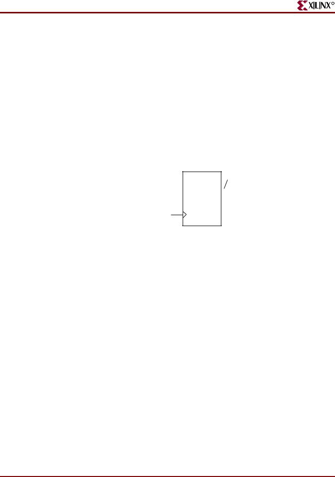
Pin Layout of SRL16E Diagram
|
D |
SRL16E |
Q |
|
|
CE |
|
|
|
|
|
|
|
|
CLK |
|
|
|
|
|
|
|
|
|
|
A0 |
|
|
|
|
|
|
|
|
|
A1 |
|
|
|
|
|
|
|
|
|
A2 |
|
|
|
|
|
|
|
|
|
A3 |
|
|
|
|
|
|
X8423 |
|
|
|
|
||
|
|
|
||
Figure 2-20: |
Pin Layout of SRL16E |
|||
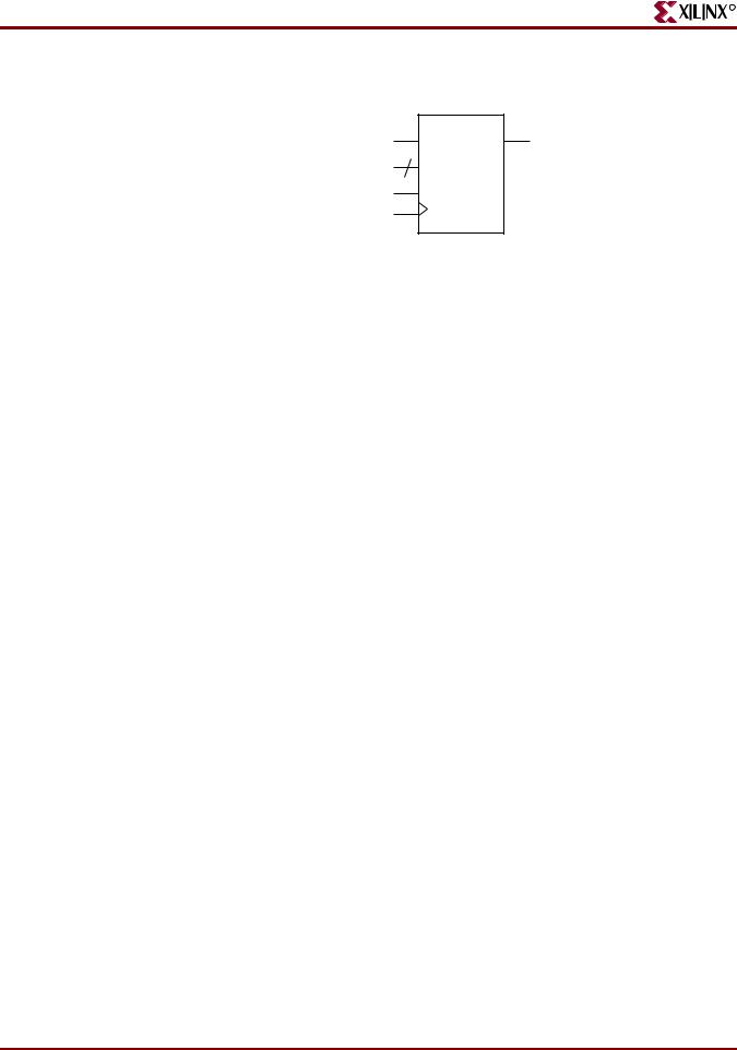
Pin Layout of SRLC16 Diagram
D |
|
|
|
Q |
|
|
|
||
CLK |
|
|
||
|
|
|||
|
|
|
||
A0 |
|
SRLC16 |
|
Q15 |
|
|
|||
A1 |
|
|
||
|
|
|||
|
|
|
|
|
|
|
|
|
|
A2 |
|
|
|
|
|
|
|
|
|
A3 |
|
|
|
X9497 |
|
|
|
||
|
|
|
|
|
|
|
|
|
|
Figure 2-21: Pin Layout of SRLC16
Shift Registers Log File
XST recognizes shift registers in the Low Level Optimization step. The XST log file reports the size of recognized shift registers.
...
=============================================
* HDL Synthesis *
=============================================
Synthesizing Unit <shift_registers_1>.
66 |
www.xilinx.com |
XST User Guide |
|
|
10.1 |

R
Shift Registers HDL Coding Techniques
Related source file is "shift_registers_1.vhd". Found 8-bit register for signal <tmp>. Summary:
inferred 8 D-type flip-flop(s). Unit <shift_registers_1> synthesized.
=============================================
* Advanced HDL Synthesis *
=============================================
Advanced HDL Synthesis Report Macro Statistics
# Registers : 8
Flip-Flops : 8
=============================================
=============================================
* Low Level Synthesis *
=============================================
Processing Unit <shift_registers_1> :
Found 8-bit shift register for signal <tmp_7>. Unit <shift_registers_1> processed.
=============================================
Final Register Report Macro Statistics
# Shift Registers : 1 8-bit shift register : 1
=============================================
...
Shift Registers Related Constraints
•“Shift Register Extraction (SHREG_EXTRACT)”
Shift Registers Coding Examples
This section gives the following Shift Registers examples:
•“8-Bit Shift-Left Register With Positive-Edge Clock, Serial In and Serial Out”
•“8-Bit Shift-Left Register With Negative-Edge Clock, Clock Enable, Serial In and Serial Out”
•“8-Bit Shift-Left Register With Positive-Edge Clock, Asynchronous Reset, Serial In and Serial Out”
•“8-Bit Shift-Left Register With Positive-Edge Clock, Synchronous Set, Serial In and Serial Out”
•“8-Bit Shift-Left Register With Positive-Edge Clock, Serial In and Parallel Out”
•“8-Bit Shift-Left Register With Positive-Edge Clock, Asynchronous Parallel Load, Serial In and Serial Out”
•“8-Bit Shift-Left Register With Positive-Edge Clock, Synchronous Parallel Load, Serial In and Serial Out”
•“8-Bit Shift-Left/Shift-Right Register With Positive-Edge Clock, Serial In and Parallel Out”
The coding examples in this section are accurate as of the date of publication. Download updates from ftp://ftp.xilinx.com/pub/documentation/misc/examples_v9.zip
XST User Guide |
www.xilinx.com |
67 |
10.1
Chapter 2: XST HDL Coding Techniques
R
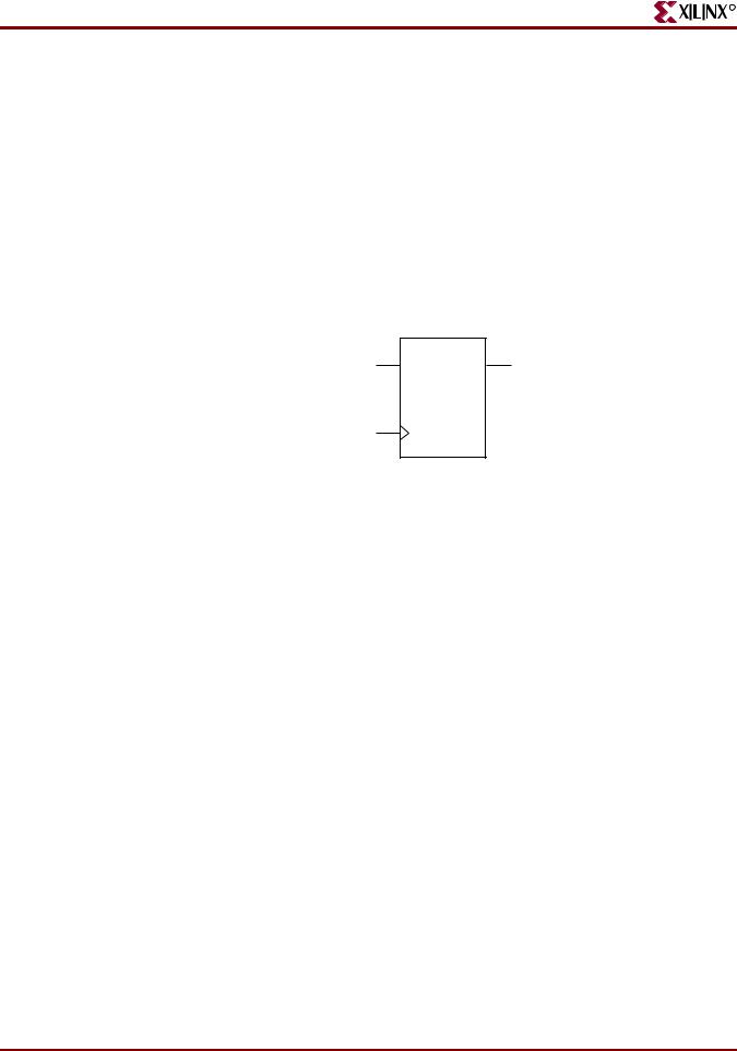
8-Bit Shift-Left Register With Positive-Edge Clock, Serial In and Serial Out
This section discusses 8-Bit Shift-Left Register With Positive-Edge Clock, Serial In and Serial Out, and includes:
•“8-Bit Shift-Left Register With Positive-Edge Clock, Serial In and Serial Out Diagram”
•“8-Bit Shift-Left Register With Positive-Edge Clock, Serial In and Serial Out Pin Descriptions”
•“8-Bit Shift-Left Register With Positive-Edge Clock, Serial In and Serial Out VHDL Coding Example”
•“8-Bit Shift-Left Register With Positive-Edge Clock, Serial In and Serial Out Verilog Coding Example”
SI |
SRL |
SO |
C
X10534
Figure 2-22: 8-Bit Shift-Left Register With Positive-Edge Clock, Serial In and Serial Out
Diagram
8-Bit Shift-Left Register With Positive-Edge Clock, Serial In and Serial Out Pin Descriptions
Table 2-23: 8-Bit Shift-Left Register With Positive-Edge Clock, Serial In and Serial Out Pin Descriptions
IO Pins |
Description |
|
|
C |
Positive-Edge Clock |
|
|
SI |
Serial In |
|
|
SO |
Serial Output |
|
|
8-Bit Shift-Left Register With Positive-Edge Clock, Serial In and Serial Out VHDL Coding Example
--
-- 8-bit Shift-Left Register with Positive-Edge Clock, Serial In, and Serial Out
--
library ieee;
use ieee.std_logic_1164.all;
entity shift_registers_1 is port(C, SI : in std_logic;
SO : out std_logic); end shift_registers_1;
68 |
www.xilinx.com |
XST User Guide |
|
|
10.1 |

R
Shift Registers HDL Coding Techniques
architecture archi of shift_registers_1 is signal tmp: std_logic_vector(7 downto 0);
begin
process (C) begin
if (C'event and C='1') then for i in 0 to 6 loop
tmp(i+1) <= tmp(i); end loop;
tmp(0) <= SI; end if;
end process;
SO <= tmp(7);
end archi;
8-Bit Shift-Left Register With Positive-Edge Clock, Serial In and Serial Out Verilog Coding Example
//
//8-bit Shift-Left Register with Positive-Edge Clock,
//Serial In, and Serial Out
//
module v_shift_registers_1 (C, SI, SO); input C,SI;
output SO; reg [7:0] tmp;
always @(posedge C) begin
tmp = {tmp[6:0], SI};
end
assign SO = tmp[7];
endmodule
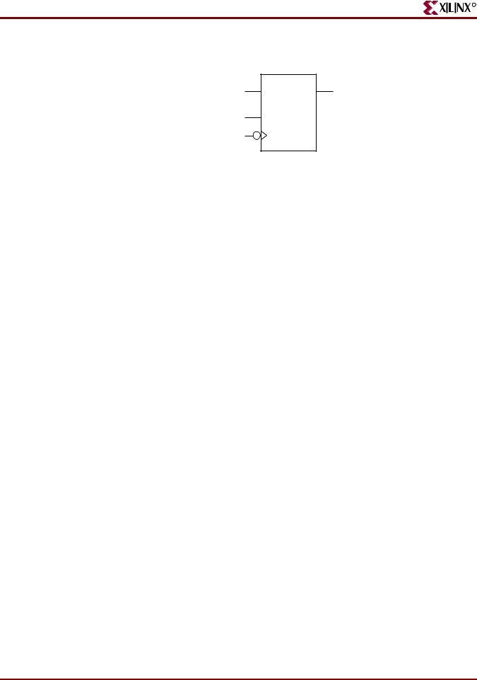
8-Bit Shift-Left Register With Negative-Edge Clock, Clock Enable, Serial In and Serial Out
This section discusses 8-Bit Shift-Left Register With Negative-Edge Clock, Clock Enable, Serial In and Serial Out, and includes:
•“8-Bit Shift-Left Register With Negative-Edge Clock, Clock Enable, Serial In and Serial Out Diagram”
•“8-Bit Shift-Left Register With Negative-Edge Clock, Clock Enable, Serial In and Serial Out Pin Descriptions”
•“8-Bit Shift-Left Register With Negative-Edge Clock, Clock Enable, Serial In and Serial Out VHDL Coding Example”
•“8-Bit Shift-Left Register With Negative-Edge Clock, Clock Enable, Serial In and Serial Out Verilog Coding Example”
XST User Guide |
www.xilinx.com |
69 |
10.1
Chapter 2: XST HDL Coding Techniques
R
SI |
SRL |
SO |
CE
C
X10535
Figure 2-23: 8-Bit Shift-Left Register With Negative-Edge Clock, Clock Enable, Serial In
and Serial Out Diagram
Table 2-24: 8-Bit Shift-Left Register With Negative-Edge Clock, Clock Enable, Serial In and Serial Out Pin Descriptions
IO Pins |
Description |
|
|
C |
Negative-Edge Clock |
|
|
SI |
Serial In |
|
|
CE |
Clock Enable (Active High) |
|
|
SO |
Serial Output |
|
|
8-Bit Shift-Left Register With Negative-Edge Clock, Clock Enable, Serial In and Serial Out VHDL Coding Example
--
--8-bit Shift-Left Register with Negative-Edge Clock, Clock Enable,
--Serial In, and Serial Out
--
library ieee;
use ieee.std_logic_1164.all;
entity shift_registers_2 is port(C, SI, CE : in std_logic;
SO : out std_logic); end shift_registers_2;
architecture archi of shift_registers_2 is signal tmp: std_logic_vector(7 downto 0);
begin
process (C) begin
if (C'event and C='0') then if (CE='1') then
for i in 0 to 6 loop tmp(i+1) <= tmp(i);
end loop; tmp(0) <= SI;
end if;
70 |
www.xilinx.com |
XST User Guide |
|
|
10.1 |
R
Shift Registers HDL Coding Techniques
end if; end process;
SO <= tmp(7);
end archi;
8-Bit Shift-Left Register With Negative-Edge Clock, Clock Enable, Serial In and Serial Out Verilog Coding Example
//
//8-bit Shift-Left Register with Negative-Edge Clock, Clock Enable,
//Serial In, and Serial Out
//
module v_shift_registers_2 (C, CE, SI, SO); input C,SI, CE;
output SO; reg [7:0] tmp;
always @(negedge C) begin
if (CE) begin
tmp = {tmp[6:0], SI};
end
end
assign SO = tmp[7];
endmodule
XST User Guide |
www.xilinx.com |
71 |
10.1
Chapter 2: XST HDL Coding Techniques
R
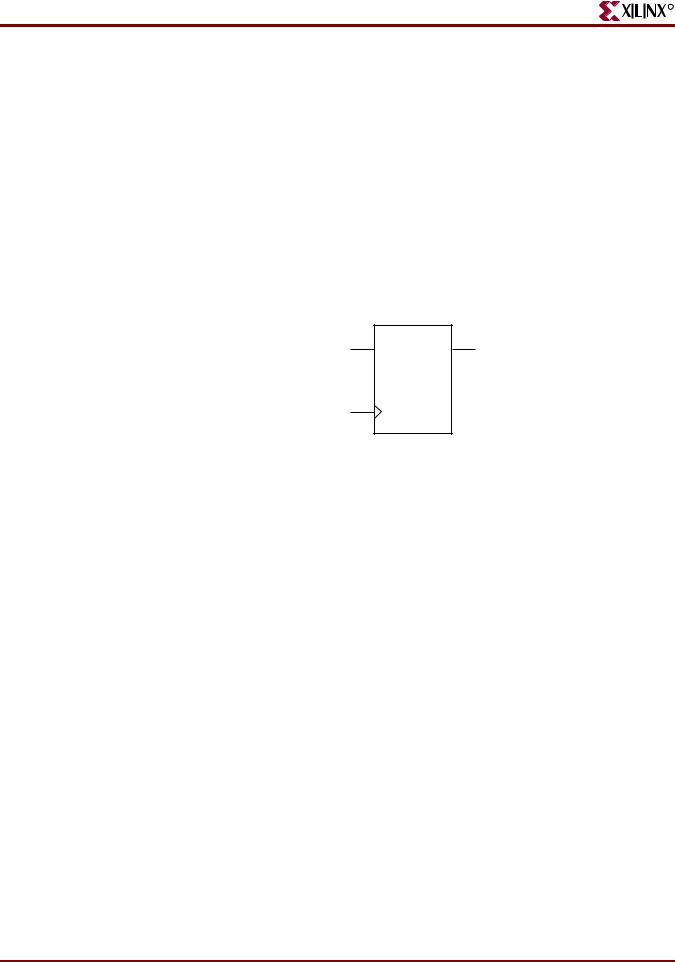
8-Bit Shift-Left Register With Positive-Edge Clock,
Asynchronous Reset, Serial In and Serial Out
This section discusses 8-Bit Shift-Left Register With Positive-Edge Clock, Asynchronous Reset, Serial In and Serial Out, and includes:
•“8-Bit Shift-Left Register With Positive-Edge Clock, Asynchronous Reset, Serial In and Serial Out Diagram”
•“8-Bit Shift-Left Register With Positive-Edge Clock, Asynchronous Reset, Serial In and Serial Out Pin Descriptions”
•“8-Bit Shift-Left Register With Positive-Edge Clock, Asynchronous Reset, Serial In and Serial Out VHDL Coding Example”
•“8-Bit Shift-Left Register With Positive-Edge Clock, Asynchronous Reset, Serial In and Serial Out Verilog Coding Example”
SHIFT
SI REG SO
C
CLR |
|
X10536 |
|
Figure 2-24: 8-Bit Shift-Left Register With Positive-Edge Clock, Asynchronous Reset,
Serial In and Serial Out Diagram
Table 2-25: 8-Bit Shift-Left Register With Positive-Edge Clock, Asynchronous Reset,
Serial In and Serial Out Pin Descriptions
IO Pins |
Description |
|
|
C |
Positive-Edge Clock |
|
|
SI |
Serial In |
|
|
CLR |
Asynchronous Reset (Active High) |
|
|
8-Bit Shift-Left Register With Positive-Edge Clock, Asynchronous Reset, Serial In and Serial Out VHDL Coding Example
--
--8-bit Shift-Left Register with Positive-Edge Clock,
--Asynchronous Reset,Serial In, and Serial Out
--
library ieee;
use ieee.std_logic_1164.all;
entity shift_registers_3 is port(C, SI, CLR : in std_logic;
SO : out std_logic); end shift_registers_3;
architecture archi of shift_registers_3 is
72 |
www.xilinx.com |
XST User Guide |
|
|
10.1 |

R
Shift Registers HDL Coding Techniques
signal tmp: std_logic_vector(7 downto 0); begin
process (C, CLR) begin
if (CLR='1') then
tmp <= (others => '0'); elsif (C'event and C='1') then
tmp <= tmp(6 downto 0) & SI; end if;
end process;
SO <= tmp(7);
end archi;
8-Bit Shift-Left Register With Positive-Edge Clock, Asynchronous Reset,
Serial In and Serial Out Verilog Coding Example
//
//8-bit Shift-Left Register with Positive-Edge Clock,
//Asynchronous Reset, Serial In, and Serial Out
//
module v_shift_registers_3 (C, CLR, SI, SO); input C,SI,CLR;
output SO; reg [7:0] tmp;
always @(posedge C or posedge CLR) begin
if (CLR)
tmp <= 8'b00000000; else
tmp <= {tmp[6:0], SI};
end
assign SO = tmp[7];
endmodule
XST User Guide |
www.xilinx.com |
73 |
10.1
Chapter 2: XST HDL Coding Techniques
R
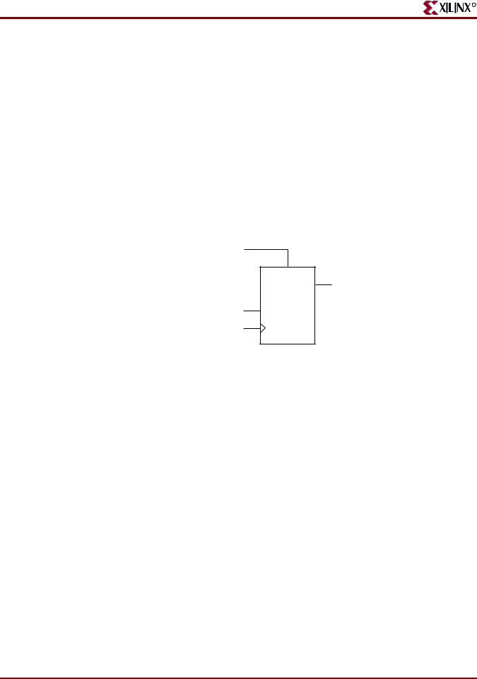
8-Bit Shift-Left Register With Positive-Edge Clock, Synchronous Set, Serial In and Serial Out
This section discusses 8-Bit Shift-Left Register With Positive-Edge Clock, Synchronous Set, Serial In and Serial Out, and includes:
•“8-Bit Shift-Left Register With Positive-Edge Clock, Synchronous Set, Serial In and Serial Out Diagram”
•“8-Bit Shift-Left Register With Positive-Edge Clock, Synchronous Set, Serial In and Serial Out Pin Descriptions”
•“8-Bit Shift-Left Register With Positive-Edge Clock, Synchronous Set, Serial In and Serial Out VHDL Coding Example”
•“8-Bit Shift-Left Register With Positive-Edge Clock, Synchronous Set, Serial In and Serial Out Verilog Coding Example”
S
SHIFT
REG SO
SI
C
X10537
Figure 2-25: 8-Bit Shift-Left Register With Positive-Edge Clock, Synchronous Set, Serial
In and Serial Out Diagram
Table 2-26: 8-Bit Shift-Left Register With Positive-Edge Clock, Synchronous Set, Serial In and Serial Out Pin Descriptions
IO Pins |
Description |
|
|
C |
Positive-Edge Clock |
|
|
SI |
Serial In |
|
|
S |
Synchronous Set (Active High) |
|
|
SO |
Serial Output |
|
|
8-Bit Shift-Left Register With Positive-Edge Clock, Synchronous Set, Serial In and Serial Out VHDL Coding Example
--
--8-bit Shift-Left Register with Positive-Edge Clock, Synchronous Set,
--Serial In, and Serial Out
--
library ieee;
use ieee.std_logic_1164.all;
74 |
www.xilinx.com |
XST User Guide |
|
|
10.1 |

R
Shift Registers HDL Coding Techniques
entity shift_registers_4 is port(C, SI, S : in std_logic;
SO : out std_logic); end shift_registers_4;
architecture archi of shift_registers_4 is signal tmp: std_logic_vector(7 downto 0);
begin
process (C, S) begin
if (C'event and C='1') then if (S='1') then
tmp <= (others => '1');
else
tmp <= tmp(6 downto 0) & SI; end if;
end if; end process;
SO <= tmp(7);
end archi;
8-Bit Shift-Left Register With Positive-Edge Clock, Synchronous Set, Serial In and Serial Out Verilog Coding Example
//
//8-bit Shift-Left Register with Positive-Edge Clock, Synchronous Set,
//Serial In, and Serial Out
//
module v_shift_registers_4 (C, S, SI, SO); input C,SI,S;
output SO; reg [7:0] tmp;
always @(posedge C) begin
if (S)
tmp <= 8'b11111111; else
tmp <= {tmp[6:0], SI};
end
assign SO = tmp[7];
endmodule
XST User Guide |
www.xilinx.com |
75 |
10.1
Chapter 2: XST HDL Coding Techniques
R
8-Bit Shift-Left Register With Positive-Edge Clock,
Serial In and Parallel Out
This section discusses 8-Bit Shift-Left Register with Positive-Edge Clock, Serial In and
Parallel Out, and includes:
•“8-Bit Shift-Left Register with Positive-Edge Clock, Serial In and Parallel Out Diagram”
•“8-Bit Shift-Left Register With Positive-Edge Clock, Serial In and Parallel Out Pin Descriptions”
•“8-Bit Shift-Left Register With Positive-Edge Clock, Serial In and Parallel Out VHDL Coding Example”
•“8-Bit Shift-Left Register With Positive-Edge Clock, Serial In and Parallel Out Verilog Coding Example”
|
|
SHIFT |
8 |
|
SI |
|
|
PO |
|
|
REG |
|
||
|
|
C
X10538
Figure 2-26: 8-Bit Shift-Left Register with Positive-Edge Clock, Serial In and Parallel Out Diagram
Table 2-27: 8-Bit Shift-Left Register With Positive-Edge Clock, Serial In and Parallel Out Pin Descriptions
IO Pins |
Description |
|
|
C |
Positive-Edge Clock |
|
|
SI |
Serial In |
|
|
PO |
Parallel Output |
|
|
8-Bit Shift-Left Register With Positive-Edge Clock, Serial In and Parallel Out VHDL Coding Example
--
--8-bit Shift-Left Register with Positive-Edge Clock,
--Serial In, and Parallel Out
--
library ieee;
use ieee.std_logic_1164.all;
entity shift_registers_5 is port(C, SI : in std_logic;
PO : out std_logic_vector(7 downto 0));
76 |
www.xilinx.com |
XST User Guide |
|
|
10.1 |

R
Shift Registers HDL Coding Techniques
end shift_registers_5;
architecture archi of shift_registers_5 is signal tmp: std_logic_vector(7 downto 0);
begin
process (C) begin
if (C'event and C='1') then tmp <= tmp(6 downto 0)& SI;
end if; end process;
PO <= tmp;
end archi;
8-Bit Shift-Left Register With Positive-Edge Clock, Serial In and Parallel Out Verilog Coding Example
//
//8-bit Shift-Left Register with Positive-Edge Clock,
//Serial In, and Parallel Out
//
module v_shift_registers_5 (C, SI, PO); input C,SI;
output [7:0] PO; reg [7:0] tmp;
always @(posedge C)
tmp <= {tmp[6:0], SI};
assign PO = tmp;
endmodule
8-Bit Shift-Left Register With Positive-Edge Clock,
Asynchronous Parallel Load, Serial In and Serial Out
This section discusses 8-Bit Shift-Left Register With Positive-Edge Clock, Asynchronous Parallel Load, Serial In and Serial Out, and includes:
•“8-Bit Shift-Left Register With Positive-Edge Clock, Asynchronous Parallel Load, Serial In and Serial Out Diagram”
•“8-Bit Shift-Left Register With Positive-Edge Clock, Asynchronous Parallel Load, Serial In and Serial Out Pin Descriptions”
•“8-Bit Shift-Left Register With Positive-Edge Clock, Asynchronous Parallel Load, Serial In and Serial Out VHDL Coding Example”
•“8-Bit Shift-Left Register With Positive-Edge Clock, Asynchronous Parallel Load, Serial In and Serial Out Verilog Coding Example”
XST User Guide |
www.xilinx.com |
77 |
10.1

Chapter 2: XST HDL Coding Techniques
R
SHIFT
SI 8 REG SO
D
ALOAD
C
X10539
Figure 2-27: 8-Bit Shift-Left Register With Positive-Edge Clock, Asynchronous Parallel
Load, Serial In and Serial Out Diagram
Table 2-28: 8-Bit Shift-Left Register With Positive-Edge Clock, Asynchronous Parallel Load, Serial In and Serial Out Pin Descriptions
IO Pins |
Description |
|
|
C |
Positive-Edge Clock |
|
|
SI |
Serial In |
|
|
ALOAD |
Asynchronous Parallel Load (Active High) |
|
|
D |
Data Input |
|
|
SO |
Serial Output |
|
|
8-Bit Shift-Left Register With Positive-Edge Clock, Asynchronous Parallel Load, Serial In and Serial Out VHDL Coding Example
--
--8-bit Shift-Left Register with Positive-Edge Clock,
--Asynchronous Parallel Load, Serial In, and Serial Out
library ieee;
use ieee.std_logic_1164.all;
entity shift_registers_6 is
port(C, SI, ALOAD : in std_logic;
D : in std_logic_vector(7 downto 0); SO : out std_logic);
end shift_registers_6;
architecture archi of shift_registers_6 is signal tmp: std_logic_vector(7 downto 0);
begin
process (C, ALOAD, D) begin
if (ALOAD='1') then tmp <= D;
elsif (C'event and C='1') then tmp <= tmp(6 downto 0) & SI;
78 |
www.xilinx.com |
XST User Guide |
|
|
10.1 |

R
Shift Registers HDL Coding Techniques
end if; end process;
SO <= tmp(7);
end archi;
8-Bit Shift-Left Register With Positive-Edge Clock, Asynchronous Parallel Load, Serial In and Serial Out Verilog Coding Example
//
//8-bit Shift-Left Register with Positive-Edge Clock,
//Asynchronous Parallel Load, Serial In, and Serial Out
module v_shift_registers_6 (C, ALOAD, SI, D, SO); input C,SI,ALOAD;
input [7:0] D; output SO; reg [7:0] tmp;
always @(posedge C or posedge ALOAD) begin
if (ALOAD) tmp <= D;
else
tmp <= {tmp[6:0], SI};
end
assign SO = tmp[7];
endmodule
8-Bit Shift-Left Register With Positive-Edge Clock,
Synchronous Parallel Load, Serial In and Serial Out
This section discusses 8-Bit Shift-Left Register With Positive-Edge Clock, Synchronous Parallel Load, Serial In and Serial Out, and includes:
•“8-Bit Shift-Left Register With Positive-Edge Clock, Synchronous Parallel Load, Serial In and Serial Out Diagram”
•“8-Bit Shift-Left Register With Positive-Edge Clock, Synchronous Parallel Load, Serial In and Serial Out Pin Descriptions”
•“8-Bit Shift-Left Register With Positive-Edge Clock, Synchronous Parallel Load, Serial In and Serial Out VHDL Coding Example”
•“8-Bit Shift-Left Register With Positive-Edge Clock, Synchronous Parallel Load, Serial In and Serial Out Verilog Coding Example”
XST User Guide |
www.xilinx.com |
79 |
10.1
Chapter 2: XST HDL Coding Techniques
R
SHIFT
SI 8 REG SO
D
SLOAD
C
X10540
Figure 2-28: 8-Bit Shift-Left Register With Positive-Edge Clock, Synchronous Parallel
Load, Serial In and Serial Out Diagram
Table 2-29: 8-Bit Shift-Left Register With Positive-Edge Clock, Synchronous Parallel
Load, Serial In and Serial Out Pin Descriptions
IO Pins |
Description |
|
|
C |
Positive-Edge Clock |
|
|
SI |
Serial In |
|
|
SLOAD |
Synchronous Parallel Load (Active High) |
|
|
D |
Data Input |
|
|
SO |
Serial Output |
|
|
8-Bit Shift-Left Register With Positive-Edge Clock, Synchronous Parallel Load, Serial In and Serial Out VHDL Coding Example
--
--8-bit Shift-Left Register with Positive-Edge Clock,
--Synchronous Parallel Load, Serial In, and Serial Out
library ieee;
use ieee.std_logic_1164.all;
entity shift_registers_7 is
port(C, SI, SLOAD : in std_logic;
D : in std_logic_vector(7 downto 0); SO : out std_logic);
end shift_registers_7;
architecture archi of shift_registers_7 is signal tmp: std_logic_vector(7 downto 0);
begin
process (C) begin
if (C'event and C='1') then if (SLOAD='1') then
tmp <= D;
else
80 |
www.xilinx.com |
XST User Guide |
|
|
10.1 |
R
Shift Registers HDL Coding Techniques
tmp <= tmp(6 downto 0) & SI; end if;
end if; end process;
SO <= tmp(7);
end archi;
8-Bit Shift-Left Register With Positive-Edge Clock, Synchronous Parallel Load, Serial In and Serial Out Verilog Coding Example
//
//8-bit Shift-Left Register with Positive-Edge Clock,
//Synchronous Parallel Load, Serial In, and Serial Out
module v_shift_registers_7 (C, SLOAD, SI, D, SO); input C,SI,SLOAD;
input [7:0] D; output SO; reg [7:0] tmp;
always @(posedge C) begin
if (SLOAD) tmp <= D;
else
tmp <= {tmp[6:0], SI};
end
assign SO = tmp[7];
endmodule
8-Bit Shift-Left/Shift-Right Register With Positive-Edge Clock, Serial In and Parallel Out
This section discusses 8-Bit Shift-Left/Shift-Right Register With Positive-Edge Clock,
Serial In and Parallel Out, and includes:
•“8-Bit Shift-Left/Shift-Right Register With Positive-Edge Clock, Serial In and Parallel Out Diagram”
•“8-Bit Shift-Left/Shift-Right Register With Positive-Edge Clock, Serial In and Parallel Out Pin Descriptions”
•“8-Bit Shift-Left/Shift-Right Register With Positive-Edge Clock, Serial In and Parallel Out VHDL Coding Example”
•“8-Bit Shift-Left/Shift-Right Register With Positive-Edge Clock, Serial In and Parallel Out Verilog Coding Example”
XST User Guide |
www.xilinx.com |
81 |
10.1

Chapter 2: XST HDL Coding Techniques
R
|
|
SHIFT |
8 |
|
SI |
|
|
PO |
|
|
REG |
|
||
|
|
|||
LEFT_RIGHT |
|
|
|
|
|
|
|
|
|
C |
|
|
|
|
|
|
|
|
X10541
Figure 2-29: 8-Bit Shift-Left/Shift-Right Register With Positive-Edge Clock, Serial In and
Parallel Out Diagram
Table 2-30: 8-Bit Shift-Left/Shift-Right Register With Positive-Edge Clock, Serial In and Parallel Out Pin Descriptions
IO Pins |
Description |
|
|
C |
Positive-Edge Clock |
|
|
SI |
Serial In |
|
|
LEFT_RIGHT |
Left/right shift mode selector |
|
|
PO |
Parallel Output |
|
|
8-Bit Shift-Left/Shift-Right Register With Positive-Edge Clock, Serial In and Parallel Out VHDL Coding Example
--
--8-bit Shift-Left/Shift-Right Register with Positive-Edge Clock,
--Serial In, and Parallel Out
--
library ieee;
use ieee.std_logic_1164.all;
entity shift_registers_8 is
port(C, SI, LEFT_RIGHT : in std_logic;
PO : out std_logic_vector(7 downto 0)); end shift_registers_8;
architecture archi of shift_registers_8 is signal tmp: std_logic_vector(7 downto 0);
begin
process (C) begin
if (C'event and C='1') then if (LEFT_RIGHT='0') then
tmp <= tmp(6 downto 0) & SI;
else
tmp <= SI & tmp(7 downto 1); end if;
end if;
82 |
www.xilinx.com |
XST User Guide |
|
|
10.1 |