

- •Analysis and Application of Analog Electronic Circuits to Biomedical Instrumentation
- •Dedication
- •Preface
- •Reader Background
- •Rationale
- •Description of the Chapters
- •Features
- •The Author
- •Table of Contents
- •1.1 Introduction
- •1.2 Sources of Endogenous Bioelectric Signals
- •1.3 Nerve Action Potentials
- •1.4 Muscle Action Potentials
- •1.4.1 Introduction
- •1.4.2 The Origin of EMGs
- •1.5 The Electrocardiogram
- •1.5.1 Introduction
- •1.6 Other Biopotentials
- •1.6.1 Introduction
- •1.6.2 EEGs
- •1.6.3 Other Body Surface Potentials
- •1.7 Discussion
- •1.8 Electrical Properties of Bioelectrodes
- •1.9 Exogenous Bioelectric Signals
- •1.10 Chapter Summary
- •2.1 Introduction
- •2.2.1 Introduction
- •2.2.4 Schottky Diodes
- •2.3.1 Introduction
- •2.4.1 Introduction
- •2.5.1 Introduction
- •2.5.5 Broadbanding Strategies
- •2.6 Photons, Photodiodes, Photoconductors, LEDs, and Laser Diodes
- •2.6.1 Introduction
- •2.6.2 PIN Photodiodes
- •2.6.3 Avalanche Photodiodes
- •2.6.4 Signal Conditioning Circuits for Photodiodes
- •2.6.5 Photoconductors
- •2.6.6 LEDs
- •2.6.7 Laser Diodes
- •2.7 Chapter Summary
- •Home Problems
- •3.1 Introduction
- •3.2 DA Circuit Architecture
- •3.4 CM and DM Gain of Simple DA Stages at High Frequencies
- •3.4.1 Introduction
- •3.5 Input Resistance of Simple Transistor DAs
- •3.7 How Op Amps Can Be Used To Make DAs for Medical Applications
- •3.7.1 Introduction
- •3.8 Chapter Summary
- •Home Problems
- •4.1 Introduction
- •4.3 Some Effects of Negative Voltage Feedback
- •4.3.1 Reduction of Output Resistance
- •4.3.2 Reduction of Total Harmonic Distortion
- •4.3.4 Decrease in Gain Sensitivity
- •4.4 Effects of Negative Current Feedback
- •4.5 Positive Voltage Feedback
- •4.5.1 Introduction
- •4.6 Chapter Summary
- •Home Problems
- •5.1 Introduction
- •5.2.1 Introduction
- •5.2.2 Bode Plots
- •5.5.1 Introduction
- •5.5.3 The Wien Bridge Oscillator
- •5.6 Chapter Summary
- •Home Problems
- •6.1 Ideal Op Amps
- •6.1.1 Introduction
- •6.1.2 Properties of Ideal OP Amps
- •6.1.3 Some Examples of OP Amp Circuits Analyzed Using IOAs
- •6.2 Practical Op Amps
- •6.2.1 Introduction
- •6.2.2 Functional Categories of Real Op Amps
- •6.3.1 The GBWP of an Inverting Summer
- •6.4.3 Limitations of CFOAs
- •6.5 Voltage Comparators
- •6.5.1 Introduction
- •6.5.2. Applications of Voltage Comparators
- •6.5.3 Discussion
- •6.6 Some Applications of Op Amps in Biomedicine
- •6.6.1 Introduction
- •6.6.2 Analog Integrators and Differentiators
- •6.7 Chapter Summary
- •Home Problems
- •7.1 Introduction
- •7.2 Types of Analog Active Filters
- •7.2.1 Introduction
- •7.2.3 Biquad Active Filters
- •7.2.4 Generalized Impedance Converter AFs
- •7.3 Electronically Tunable AFs
- •7.3.1 Introduction
- •7.3.3 Use of Digitally Controlled Potentiometers To Tune a Sallen and Key LPF
- •7.5 Chapter Summary
- •7.5.1 Active Filters
- •7.5.2 Choice of AF Components
- •Home Problems
- •8.1 Introduction
- •8.2 Instrumentation Amps
- •8.3 Medical Isolation Amps
- •8.3.1 Introduction
- •8.3.3 A Prototype Magnetic IsoA
- •8.4.1 Introduction
- •8.6 Chapter Summary
- •9.1 Introduction
- •9.2 Descriptors of Random Noise in Biomedical Measurement Systems
- •9.2.1 Introduction
- •9.2.2 The Probability Density Function
- •9.2.3 The Power Density Spectrum
- •9.2.4 Sources of Random Noise in Signal Conditioning Systems
- •9.2.4.1 Noise from Resistors
- •9.2.4.3 Noise in JFETs
- •9.2.4.4 Noise in BJTs
- •9.3 Propagation of Noise through LTI Filters
- •9.4.2 Spot Noise Factor and Figure
- •9.5.1 Introduction
- •9.6.1 Introduction
- •9.7 Effect of Feedback on Noise
- •9.7.1 Introduction
- •9.8.1 Introduction
- •9.8.2 Calculation of the Minimum Resolvable AC Input Voltage to a Noisy Op Amp
- •9.8.5.1 Introduction
- •9.8.5.2 Bridge Sensitivity Calculations
- •9.8.7.1 Introduction
- •9.8.7.2 Analysis of SNR Improvement by Averaging
- •9.8.7.3 Discussion
- •9.10.1 Introduction
- •9.11 Chapter Summary
- •Home Problems
- •10.1 Introduction
- •10.2 Aliasing and the Sampling Theorem
- •10.2.1 Introduction
- •10.2.2 The Sampling Theorem
- •10.3 Digital-to-Analog Converters (DACs)
- •10.3.1 Introduction
- •10.3.2 DAC Designs
- •10.3.3 Static and Dynamic Characteristics of DACs
- •10.4 Hold Circuits
- •10.5 Analog-to-Digital Converters (ADCs)
- •10.5.1 Introduction
- •10.5.2 The Tracking (Servo) ADC
- •10.5.3 The Successive Approximation ADC
- •10.5.4 Integrating Converters
- •10.5.5 Flash Converters
- •10.6 Quantization Noise
- •10.7 Chapter Summary
- •Home Problems
- •11.1 Introduction
- •11.2 Modulation of a Sinusoidal Carrier Viewed in the Frequency Domain
- •11.3 Implementation of AM
- •11.3.1 Introduction
- •11.3.2 Some Amplitude Modulation Circuits
- •11.4 Generation of Phase and Frequency Modulation
- •11.4.1 Introduction
- •11.4.3 Integral Pulse Frequency Modulation as a Means of Frequency Modulation
- •11.5 Demodulation of Modulated Sinusoidal Carriers
- •11.5.1 Introduction
- •11.5.2 Detection of AM
- •11.5.3 Detection of FM Signals
- •11.5.4 Demodulation of DSBSCM Signals
- •11.6 Modulation and Demodulation of Digital Carriers
- •11.6.1 Introduction
- •11.6.2 Delta Modulation
- •11.7 Chapter Summary
- •Home Problems
- •12.1 Introduction
- •12.2.1 Introduction
- •12.2.2 The Analog Multiplier/LPF PSR
- •12.2.3 The Switched Op Amp PSR
- •12.2.4 The Chopper PSR
- •12.2.5 The Balanced Diode Bridge PSR
- •12.3 Phase Detectors
- •12.3.1 Introduction
- •12.3.2 The Analog Multiplier Phase Detector
- •12.3.3 Digital Phase Detectors
- •12.4 Voltage and Current-Controlled Oscillators
- •12.4.1 Introduction
- •12.4.2 An Analog VCO
- •12.4.3 Switched Integrating Capacitor VCOs
- •12.4.6 Summary
- •12.5 Phase-Locked Loops
- •12.5.1 Introduction
- •12.5.2 PLL Components
- •12.5.3 PLL Applications in Biomedicine
- •12.5.4 Discussion
- •12.6 True RMS Converters
- •12.6.1 Introduction
- •12.6.2 True RMS Circuits
- •12.7 IC Thermometers
- •12.7.1 Introduction
- •12.7.2 IC Temperature Transducers
- •12.8 Instrumentation Systems
- •12.8.1 Introduction
- •12.8.5 Respiratory Acoustic Impedance Measurement System
- •12.9 Chapter Summary
- •References

482 |
Analysis and Application of Analog Electronic Circuits |
12.4 Voltage and Current-Controlled Oscillators
12.4.1Introduction
The voltage-controlled oscillator (VCO) (or current controlled oscillator, CCO) is an important subsystem in many electronic devices and systems. It is an important component system in the phase-lock loop, as well as in certain communication and instrumentation systems. VCOs and CCOs can have sinusoidal, triangular, or TTL outputs of constant amplitude. The frequency of a VCO or CCO in its linear range can be expressed by:
fo = KV VC + b Hz |
(12.21A) |
fo = KC IC + b |
(12.21B) |
The frequency constants, KV and KC, can have either sign, as can the intercept, b. It is desirable that a VCO have a wide linear operating range =
[(fomax − fomin)/(fomax + fomin)]; low noise (phase and amplitude); low tempco ( fo T)(1/fo); and a high spectral purity (low THD) if it produces a sinusoidal
output. (Many VCOs produce TTL outputs, or triangle wave outputs.) There are many architectures for VCOs. The first examined is a “linear
amplifier” oscillator in which fo is tuned by two variable-gain elements that can be analog multipliers or multiplying digital-to-analog converters (MDACs).
12.4.2An Analog VCO
Figure 12.15 shows the schematic of an electronically tuned VCO based on the use of linear circuit elements connected in a positive feedback loop (Northrop, 1990). The block diagram below the schematic illustrates the transfer functions of the two minor loops whose poles are set by the dc voltage VC input to the two analog multipliers. After the two minor loops are reduced, the oscillator’s loop gain can be written as:
AL (s) = |
+s kVC (10RC) |
|
(12.22) |
|
s2 + s 2V |
(10RC) + V2 |
(10RC)2 |
||
|
C |
C |
|
|
From Section 5.5 on oscillators in Chapter 5, it can be seen that the rootlocus diagram for this oscillator is a circle centered on the origin. The locus branches for the closed-loop poles begin at s = −VC (10RC) r/s, cross the jω axis in the s-plane at s = ±jωo when k = 2, and hit the positive real axis at s = +ωo. Then, one branch approaches the zero at the origin while the other branch goes toward +• as k increases.
© 2004 by CRC Press LLC
Examples of Special Analog Circuits and Systems |
483 |
||
R |
|
|
R + αV4 |
R |
|
C |
kR |
V1 R |
AM1 |
R |
R |
V2 |
|
V3 |
V4 |
+ |
|
|
|
|
− |
|
|
|
|
VC > 0 |
|
|
− |
V7 |
R |
|
|
||
+ |
|
|
|
|
|
C |
R |
|
AM2 |
R |
V5 |
|
|
||
V1’ |
C |
|
|
|
V6 |
V1 |
|
|
− VC /(10RC) |
|
s + VC /(10RC) |
||
|
|
||
V1’ |
|
|
s |
|
|
||
|
|
||
|
s + VC /(10RC) |
||
|
|
||
|
|
|
|
V4 |
V5 |
|
− k |
FIGURE 12.15
Schematic of a voltage-tuned oscillator using positive feedback. The tungsten filament lamp is used to limit and stabilize oscillation amplitude. A systems block diagram of the linear part of the oscillator is shown below the schematic. See text for analysis.
Using the venerable Barkhausen criterion (Millman, 1979) for oscillation on this oscillator:
AL (jωo ) ∫ 1–0∞ = |
|
|
jωokVC (10RC) |
|
(12.23) |
||
−ω2 |
+ V2 |
(10RC)2 + jω |
o |
2V |
(10RC) |
||
|
o |
C |
|
C |
|
|
|
Clearly, the real terms in the denominator must sum to zero. This condition gives the radian oscillation frequency,
ωo = VC (10RC) r s , |
(12.24) |
© 2004 by CRC Press LLC

484 |
Analysis and Application of Analog Electronic Circuits |
and the minimum gain for oscillation, k = 2. Thus, VC can set ωo over a wide range, e.g., 0.01 ≤ VC ≤ 10 V, or a 1:1000 range. For practical reasons, make k > 2 and use a PTC tungsten lamp instead of the input R to the third op amp. Now the overall gain of this stage is:
V5 |
= − |
k R |
= −2 |
(12.25) |
V4 |
|
|||
|
R + αV4 |
|
||
If k = 4 is set, then the steady state, equilibrium value of V4 is found to be R/α for any ωo. Making k = 4 allows the oscillations to grow rapidly to the equilibrium level.
12.4.3Switched Integrating Capacitor VCOs
Certain VCOs can simultaneously output TTL pulses, a triangle wave, and a sine wave of the same frequency. An example of this type of VCO is the Exar XR8038 waveform generator, which works over a range of millihertz to approximately 1 MHz with proper choice of timing capacitor, CT. A newer version of the XR8038 is the Maxim MAX038 VFC, which can generate various waveforms from 1 mHz to 20 MHz.
Figure 12.16 illustrates the organization of a generic switched integrating capacitor VCO. Assume that Vin > 0. At t = 0, the MOS switch is in position u and the capacitor is charged by current GmVin, so VT goes from 0 to VT = φ+ when the output of the upper comparator goes HI, which makes the RS flip-flop Q output go HI, causing the MOS switch to go to position d. In position d, the capacitor CT is discharged by a net current, −GmVin, causing VT to ramp down to φ− < 0. When VT reaches φ−, the output of the lower comparator goes high, causing the RSFF Q output to go LO, which switches the MOS switch to u again, causing the capacitor to charge positively again from current GmVin, etc.
Vin is the controlling input to the two VCCSs. Note that the capacitor CT integrates the current:
VT = (1 CT ) iC dt |
(12.26) |
Thus, from the VT triangle waveform, it is easy to find the frequency of oscillation:
f = 1 T = |
GmVin |
Hz |
(12.27) |
|
4C φ |
||||
|
|
|
||
|
T |
|
|
In Equation 12.27, φ = φ+ = −φ− > 0 was assumed.
© 2004 by CRC Press LLC

Examples of Special Analog Circuits and Systems |
485 |
|
sin(*) NL |
φ+
Vcc
VCCS
GmVin
VT
Vin |
VT |
× 1 Buff
CT
d
u
φ− < 0
MOS SW
Sine out
Triangle out |
× 1 Buff
Comp.
RSFF
R Q TTL out
S
Comp.
VCCS 2GmVin
VT |
MOS SW to d |
|
|
|
φ+ |
|
|
0 |
T/4 |
T |
t |
|
|
|
|
|
φ− |
|
|
MOS SW to u
FIGURE 12.16
Block diagram of a switched integrating capacitor VCO.
Note that this VCO produces simultaneous sine, triangle, and TTL outputs. The sinusoidal output is derived from the buffered capacitor waveform, VT, by passing it through a diode wave-shaper, sin(*) NL. This type of VCO is often used as the basis for laboratory function generators.
12.4.4The Voltage-Controlled, Emitter-Coupled Multivibrator
Figure 12.17 illustrates the simplified schematic of another popular VCO architecture. This astable, emitter-coupled multivibrator (AMV) derives its frequency control from the transistors Q5 and Q6, which act as VCCSs and control the rate that CT charges and discharges and, thus, the AMV’s frequency. This architecture is inherently very fast; versions of it using MOSFETs have been used to build a VCO with an 800-MHz tuning range that operates in excess of 2.5 GHz (Herzel et al., 2001).
The heart of this VCO is the free-running, astable multivibrator (AMV), which alternately switches Q1 and Q2 on and off as the timing capacitor charges and discharges. Detailed analysis of this circuit can be found in
© 2004 by CRC Press LLC

486 |
Analysis and Application of Analog Electronic Circuits |
Vcc
R |
D1 |
D2 |
R |
Vo |
Q3 |
Q4 |
|
Q1 |
|
|
Q2 |
|
Ibias |
Ibias |
|
|
VC |
|
|
|
+ |
− |
|
|
CT |
|
gmVin |
Q5 |
gmVin |
|
|
|
|
Q6 |
Vin
RE RE
FIGURE 12.17
Simplified schematic of a voltage-controlled, emitter-coupled, (astable) multivibrator (VCECM).
Franco (1988) and in Gray and Meyer (1984). Analysis is helped by considering the circuit of Figure 12.18 and the waveforms of Figure 12.19. According to analysis by Gray and Meyer:
We calculate the period [frequency] by first assuming that Q1 is turned off and Q2 is turned on. The circuit then appears as shown in [Figure 12.18]. We assume that current I [Ic2 ] is large so that the voltage drop IR is large enough to turn on diode [D2]. Thus the base of Q4 is one diode drop below VCC, the emitter is two diode drops below VCC, and the base of Q1 is two diode drops below VCC. If we can neglect the base current of Q3, its base is at VCC and its emitter is one diode drop below VCC. Thus the emitter of Q2 is two diode drops below VCC. Since Q1 is off, the current I1 [gmVin] is charging the capacitor so that the emitter of Q1 is becoming more negative. Q1 will turn on when the voltage at its emitter becomes equal to three diode drops below VCC. Transistor Q1 will then turn on, and the resulting collector current in Q1 turns on [D1]. As a result, the base of Q3 moves in the negative direction by one diode drop, causing the base of Q2 to move in the negative direction by one diode drop. Q2 will turn off, causing the base of Q1 to move positive by one diode drop because [D2] also turns off. As a result, the emitter-base junction of Q2 is reverse-biased by one diode drop because the voltage on CT cannot
© 2004 by CRC Press LLC
Examples of Special Analog Circuits and Systems |
487 |
Vcc
R |
D1 |
D2 |
R |
Vo |
Q3 |
Q4 |
|
Q1 |
(off) |
|
Q2 |
Ibias Ibias
IE2 = 2gmVin
VC
+−
gmVin |
CT |
Q5 |
Q6 |
gmVin |
gmVin |
FIGURE 12.18
The VCECM charging CT with Q1 OFF.
change instantaneously. Current [gmVin] must now charge the capacitor voltage in the negative direction by an amount equal to two diode drops before the circuit will switch back again. Since the circuit is symmetrical, the half period is given by the time required to charge the capacitor and is:
T 2 = Q (gmVin ) |
= |
CT |
2VBE(on) |
(12.28) |
|||||
|
gmVin |
||||||||
|
|
|
|
|
|
|
|||
where Q = CT V = CT 2VBE(on) is the charge on the capacitor. The frequency |
|||||||||
of the oscillator [VCECM] is thus: |
|
|
|
|
|
||||
f = |
1 |
= |
|
gmVin |
|
|
(12.29) |
||
T |
CT 4VBE(on) |
||||||||
|
|
|
|||||||
Note the similarity between Equation 12.29 and Equation 12.27 and that the AMV is a regenerative positive feedback circuit when it is switching. The complementary state changes of Q1 and Q2 are made more rapid by the positive feedback.
Figure 12.20 illustrates the use of two nose-to-nose varactor diodes (also called epicap diodes by Motorola) to tune an MC1648 emitter-coupled multivibrator VCO. A varactor diode (VD) is a reverse-biased Si pn junction diode, characterized by a voltage-variable depletion capacitance modeled by:
© 2004 by CRC Press LLC

488 |
Analysis and Application of Analog Electronic Circuits |
Vb2 |
Vcc |
Vcc − VBE |
Vcc − 2VBE |
VBE 0.6 V |
t |
0 |
Ve2 |
Vcc |
Vcc − VBE |
Vcc − 2VBE |
Vcc − 3VBE |
0 |
VC |
0.6 |
0 |
−0.6 |
Vo (VC3) |
|
|
Vcc |
|
|
Q1 OFF |
Q2 OFF |
Q1 OFF |
Vcc − VBE |
|
|
0 |
|
|
FIGURE 12.19
Relevant waveforms in the VCECM for two cycles of oscillation.
Cvo |
|
|
Cv = (1− VD ψo )γ , VD |
< 0. |
(12.30) |
where Cvo is the diode’s junction capacitance at VD = 0, ψo is the “built-in barrier potential,” typically on the order of 0.75 V for a Si diode at room temperature, and γ is the capacitance exponent. γ can vary from approximately 1/3 to 2, depending on the doping gradients at the junction boundary and can be shown to be 0.5 for an abrupt (step) junction (Gray and Meyer, 1984).
The output of the MC1648 oscillator is an emitter-coupled logic (ECL) square wave; frequencies as high as 225 MHz can be obtained with this IC,
© 2004 by CRC Press LLC

Examples of Special Analog Circuits and Systems |
489 |
|
|
Vc |
|
5 µF |
0.1 µF |
|
MC1648 ECO
51 kΩ
VD 
Vo
L
VD 
L = 5 T #20 Cu wire on
MicroMetal #T30-13 µ
toroidal core
0.1 F
VD = MV1404 varactor diode
 fo (MHz)
170
150
fo 15Vc + 20 MHz, (2 ≤ Vc ≤ 10 V)
130
110
90
70
Vc
50
0 |
2 |
4 |
6 |
8 |
10 |
FIGURE 12.20
Top: A VCO that uses the voltage-variable capacitance of two varactor diodes to set its output frequency. Bottom: The frequency vs. dc control voltage characteristic of the varactor VCO.
which can serve as the VCO in a PLL. In the circuit shown, the tuning range lies between VD = −2 to –10 V (or 2 ≤ Vc ≤ 10 V). The actual fo(Vc) curve is sigmoid, but can be approximated by the linear VCO relation,
fo 15Vc + 20 MHz, |
(12.31) |
over the range of Vc shown. Note that two VDs are used in series to halve their capacitance, seen in the resonant “tank” circuit. A Motorola MV1404 VD’s capacitance goes from 160 pF at VD = −1 to approximately 11 pF at VD = −10 V.
© 2004 by CRC Press LLC
490 |
Analysis and Application of Analog Electronic Circuits |
12.4.5The Voltage-to-Period Converter and Applications
The voltage-to-period converter (VPC) is a variable frequency oscillator in which the period of the oscillation, T, is directly proportional to the controlling voltage, Vc. Mathematically, this is simply stated as:
T = KP Vc + b seconds |
(12.32) |
Here b is a positive constant and KP is the VPC constant in seconds per volt. Practical considerations dictate lower and upper bounds to T. Obviously, the VPC’s output frequency is 1/T Hz. The conventional voltage-to-frequency converter (VFC) has its output frequency directly proportional to its input voltage (or current),
fo = KV Vc + d |
(12.33) |
KV is the VCO constant in Hertz per volt and d is a constant (Hertz).
In several important instrumentation applications, use of a VPC (rather than a VFC) linearizes the measurement system output; several examples are described next.
Realization of VPCs. As has been shown, many IC manufacturers make VFC VCOs. Some have TTL outputs; others generate sine, triangle, and TTL outputs. No one, to this author’s knowledge, markets a VPC IC. One obvious way to make a VPC is to take a VFC in which fo = KVVc + d and use a nonlinear analog circuit to process the input, V1, so that the net result is a VPC. Mathematically,
T = KPV1 |
+ b = |
1 |
|
(12.34) |
KV V2 |
|
|||
|
|
+ d |
||
To find the required nonlinearity, solve Equation 12.34 for V2 = f (V1). This gives:
V2 |
= |
1− bd − d KPV1 |
(12.35) |
||
KV (KPV1 |
+ b) |
||||
|
|
|
|||
Considerable simplification accrues if a VFC with d = 0 is used. Now the nonlinearity needs to be:
V2 |
= |
1 |
|
(12.36) |
|
KV (KPV1 |
+ b) |
||||
|
|
|
Figure 12.21 illustrates an op amp circuit that will generate the requisite V2 for the VFC to produce a VPC. Note that V3 must be >0 and VR = +0.1 V.
© 2004 by CRC Press LLC

Examples of Special Analog Circuits and Systems |
491 |
||
1V |
|
|
|
RKP /b |
RKVKP |
R |
|
R |
|
R |
|
V1
V3 = KV (KPV1 + b)
V2V3/10 |
Analog multiplier |
|
V2 |
Vo, f |
|
VFC |
||
|
VR +
FIGURE 12.21
Schematic of a nonlinear op amp circuit used to make a voltage-to-period converter from a conventional voltage-to-frequency converter.
Another approach to building a VPC used in the author’s laboratory is shown in Figure 12.22. Here the differential output of a NOR gate RS flipflop is integrated by a high slew rate op amp. Assume output C of the FF is high. The op amp output voltage ramps up at a slope fixed by the voltage difference at the FF outputs (e.g., 4 V) times 1/RC of the integrator. When Vo reaches the variable threshold, VC, the upper AD 790 comparator goes low, triggering the upper one-shot to reset the FF output C to low. Now Vo ramps down until it reaches the fixed −10-V threshold of the lower comparator. The lower comparator goes high, triggering the lower one-shot to set FF output C high again, etc. The two-input NOR gate gives a VPC output pulse at every FF state transition. The AD 840 op amp has a slew rate of 400 V/μs, or 4.E 8 V/s. It is connected as a differential integrator.
In this VPC design, VC varies over −9 ≤ Vc ≤ + 10 V. Choose R = 1 k, C = 850 pF, and let the FF’s V = 4 V. These data show that Vo ramps up or down with a slope of m = V/RC = 4.71E6 V/s. Now when Vc = 0, T = b = 2.125E–6 sec and KP = 2.125E−7. It is easy to see that the maxT = 20 V 4.71E6 = 4.250E–6
sec and fmin = 2.353E5 Hz. Likewise, the minT = 1 V/4.71E6 = 2.125E−7 sec and fmax = 4.71 MHz.
Applications. A VFC or a VPC can be used as the signal source in a closedloop, constant-phase velocimeter and ranging system (Northrop, 2002). However, as will be shown later and in Section 12.8.3, the use of a VPC produces a linear range output and a velocity signal independent of range, while the use of a VFC produces a nonlinear range output and a rangedependent velocity signal.
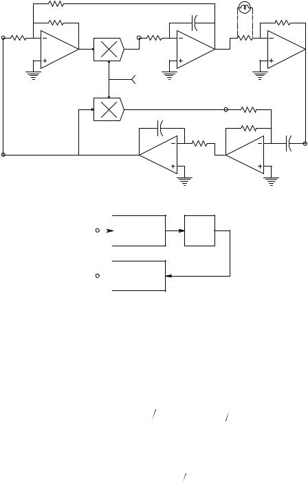
The basic architecture of a type 1 closed-loop, constant-phase laser velocimeter and ranging system is shown in Figure 12.23. This system uses narrow,
© 2004 by CRC Press LLC

492 |
Analysis and Application of Analog Electronic Circuits |
||||
|
+ 5 V |
|
|
|
|
|
B |
Q |
|
|
Vc |
|
O/S |
|
AD 790 |
||
|
|
|
|||
|
|
|
D |
|
C |
|
RST |
|
|
R |
|
|
|
|
|
||
|
|
|
|
|
Vo |
|
|
|
|
R |
AD 840 |
|
|
|
|
(Differential |
|
|
|
|
|
|
|
|
|
|
|
|
integrator) |
|
|
|
C |
|
C |
|
RST |
|
|
|
|
|
|
|
|
|
|
|
A |
Q |
O/S |
|
AD 790 |
|
|
|
|||
|
|
|
|
|
−10 V |
|
|
|
E |
|
|
Vo
+ 10 V
Vc
0
− 10 V 


T
A
B
E
FIGURE 12.22
Top: Schematic of a hybrid VPC with digital output. Bottom: Waveforms of the hybrid VPC.
periodic pulses of IR laser light reflected from a moving target. The system’s feedback automatically adjusts the pulse repetition rate so that a preset phase lag is always maintained between the transmitted and received optical pulses. The system is unique in that it simultaneously outputs voltages proportional to target range and velocity. The emitted radiation of this type of system can also be CW or pulsed sound or ultrasound, or pulsed or
© 2004 by CRC Press LLC

Examples of Special Analog Circuits and Systems |
493 |
||
O/S |
PA |
|
v |
|
IRLAD |
L |
|
|
|
|
|
|
PrA |
|
L |
|
|
|
|
|
APD |
|
|
Comp. |
|
O/S |
Moving |
|
reflecting |
||
|
|
|
|
|
|
φe |
target |
VTH |
|
PD |
Kd |
Comp. |
|
O/S |
|
VPC |
Vc |
Ki |
Vφ |
|
s |
|
|
|
− |
− |
|
|
|
||
Vr |
VL |
Vset |
|
VV |
FIGURE 12.23
Block diagram of a closed-loop, constant-phase pulsed laser velocimeter and ranging system devised by the author.
amplitude-modulated microwaves, as well as photonic energy. Such systems have wide applications, ranging from medical diagnostics to weapons systems.
In the steady state, for a fixed target range, Lo, the period (or frequency) output of the VPC oscillator reaches a value so that a fixed phase lag, φm, exists between the received and transmitted signals. When φe = φm, the input to the integrator is zero and the integrator output voltage, VL, can be shown to be:
VL = KR Lo |
(12.37) |
The range constant, KR, is derived later.
If the reflecting object is moving at constant velocity, directly away from |
|
· |
|
or toward the transducers, v = ±dL/dt = ±L, then it is easy to show that the |
|
input voltage to the integrator, VV, is given by: |
|
VV = KS v |
(12.38) |
If a VPC is used, KS is independent of L. In this example, to facilitate heuristic analysis, neglect the propagation delays inherent to logic elements and analog signal conditioning pathways. The type 1 feedback system shown in Figure 12.23 uses pulsed laser light to measure the distance L to a stationary reflective target. The nominal phase lag between received and transmitted pulses is simply:
φe = 360 (2L/c)(1/T) degrees |
(12.39) |
© 2004 by CRC Press LLC

494 |
Analysis and Application of Analog Electronic Circuits |
where c is the velocity of light in m/s, T is the VPC output period, and (2L/c) is the round-trip time for a pulse reflected from the target. The phase detector module produces an output voltage with an average value of:
Vφ = Kd φe |
(12.40) |
Kd has the dimensions of volts per degree. A dc voltage, Vset, is subtracted from Vφ, so:
VV = Vφ − Vset |
(12.41) |
VV is the input to the integrator whose output, VL , is added to −Vr to give the input to the VPC, VC. Because the closed-loop system is type 1, in the steady state, VV 0. Thus,
Vset = Kd φm = Kd [360(2L c)(1 T)]= Kd [360(2L
 c)f ]
c)f ]
Thus, the steady-state phase lag is simply:
φe = φm = Vset Kd degrees
The VPC steady-state period is found from Equation 12.42 to be:
T |
= K V + b = |
720 L |
seconds |
|
c φmss |
||||
ss |
P C |
|
||
|
|
|
From the preceding equation, the VPC input voltage is:
V = |
720 L |
− b K |
|
volts |
|
P |
|||
C |
c φmss KP |
|
||
|
|
|
||
If Vr = b/KP, then VL is directly proportional to L:
VL |
= |
720 |
|
L volts. |
|
c KP (Vset |
Kd ) |
||||
|
|
|
(12.42)
(12.43)
(12.44)
(12.45)
(12.46)
Now consider the situation in which the reflecting target is approaching
·
the transducers at constant velocity, v c. Because VL = (Ki s) VV and v = L, it is possible to write in the time domain:
˙ |
|
720 Kd |
|
|
|
VV = Vo |
Ki = v |
|
volts |
(12.47) |
|
c KP Vset Ki |
|||||
|
|
|
|
Thus, a simple type 1 closed-loop, constant phase system can provide simultaneous voltage outputs that estimate target range and velocity in a linear manner.
© 2004 by CRC Press LLC