

30 |
Analysis and Application of Analog Electronic Circuits |
This is a relatively enormous small-signal capacitance that appears in parallel with the diode model. The capacitance, CD, affects the speed at which the diode can turn off. However, the forward-biased diode has the time constant:
τd = CD gd = 1.92 E-7 (1 E-2 (2 ∞ 0.026)) 1 μs |
(2.11) |
which is basically the mean minority carrier lifetime, τ. Thus, CD has little effect on mid-frequency, small-signal performance, but the stored charge does affect the time to stop conducting when vD goes step negative.
Figure 2.5 illustrates the current, voltage, and excess minority charge waveforms in the n-material for a pn junction diode in which a step of forward voltage is followed by a step of reverse voltage. Note that VD remains at the forward value following switching to VR until all the excess minority carriers have been discharged from CD. Then VD −VR and depletion capacitance dominates the junction behavior. The storage time is on the order of nanoseconds for most small-signal Si, pn diodes.
2.2.4Schottky Diodes
The Schottky barrier diode (SBD), also called a hot carrier diode, consists of a rectifying, metal insulator–semiconductor (MIS) junction. SBDs actually predate pn junction diodes by about 50 years. The first detectors in early crystal set radios were “cat’s whisker” diodes, in which a fine lead wire made contact with a metallic mineral crystal, such as galena, silicon, or germanium. Such cat’s whisker detectors were, in fact, primitive SBDs. Because their rectifier characteristics were not reproducible, cat’s whisker SBDs were only suited for early radio experimenters and were replaced by pn junction diodes in the 1950s.
The presence of a very thin, insulating interfacial oxide layer from 0.5 to 1.5 nm thick between the metal and the semicon makes a modern SBD different from an ordinary ohmic, metal–semiconductor connection. Figure 2.6 shows the static I–V characteristics of a pn diode and an SBD. Note that the SBD has a lower cut-in voltage (approximately 0.3 V) than the pn diode (approximately 0.55 V) as well as about 1000 times the reverse leakage current (0.1 μA vs. 1 nA), which does not saturate. A schematic cross section of an SBD (after Boylstead and Nashelsky, 1987) is shown on the figure.
The SBD is a majority carrier device; a pnD is a minority carrier device. In order for a pnD to block reverse current, the stored minority carriers must be swept out of the junction by the reverse electric field. This discharging limits the turn-off time to microseconds. On the other hand, the SBD has no minority carrier storage and can switch off in tens of nanoseconds, meaning the SBD can rectify currents in the hundreds of megahertz. Figure 2.7 shows a high-frequency SSM for the SBD when conducting. Note that the SS forward
© 2004 by CRC Press LLC
Models for Semiconductor Devices Used in Analog Electronic Systems |
31 |
|
|
G |
|
|
|
F |
R |
|
|
|
R |
|
+ |
|
|
|
|
|
|
|
+ |
ID(t) |
VD(t) |
|
|
VF |
|
||
|
VR |
|
|
|
|
|
+ |
|
|
Qx(t) |
|
|
|
|
IF τp |
|
|
|
|
τp |
ID(t) |
|
|
|
VF /R |
|
τpQx(t) |
|
|
|
|
Irs |
t |
|
|
|
|
||
|
|
ID(t) |
|
|
|
|
−VR /R |
|
|
VD(t) |
|
Storage |
|
|
|
|
time |
|
|
|
VDSS |
|
|
t |
|
|
tr |
|
|
−VR |
|
|
|
|
FIGURE 2.5
Schematic showing the effect of switching a diode from vD = 0, iD = 0, to forward conduction. With VF applied, vD quickly rises to the steady-state forward drop, vDSS 0.7 V, and the XS minority carriers build up to a charge, Qx. When the applied voltage is switched to −VR, a finite time is required for Qx to be dissipated before the diode can block current. During this storage time, vD remains at vDSS.
resistance, rd, and the junction capacitance, CJ, are dependent on iD and vD, respectively. Hewlett–Packard hot carrier diodes of the 5082-2300 series have reverse currents of approximately 50 to 100 nA at vD = −10 V, and CJ = 0.3
pF at vD = −10 V.
Besides high-frequency rectification and detection, SBDs can be used to speed up transistor switching in logic gates. Figure 2.8 illustrates a SBD placed in parallel with the pn base-to-collector diode in an npn BJT. In normal
© 2004 by CRC Press LLC
32 |
Analysis and Application of Analog Electronic Circuits |
|
Anode (+) |
iD |
|
iD |
|
Metal |
|
|
|
(mA) |
|
|
|
|
2.0 |
|
|
|
|
|
|
|
|
Oxide |
|
|
|
|
|
insulator |
|
|
|
SBD |
pnD |
Thin oxide |
n-Si |
|
SBD |
|
|
film |
|
|
|
|
|
|
Cathode (−) |
|
Metal |
1.0 |
|
|
|
|
|
|
pnD |
|
|
|
|
≈ 1 nA |
vD < 0 |
|
|
vD |
|
0.2 |
0.4 |
0.6 |
(V) |
≈ 0.1 A |
|
|
|
|
SBD |
|
|
|
|
FIGURE 2.6
The static I–V curves of a Schottky barrier diode and a pn junction diode.
|
3 nH |
Ls |
iD |
|
|
+ |
7 Ω |
rs |
|
|
Cp |
vD |
CJ = f(vD) |
0.15 pF |
|
||
− |
|
|
|
rd = f(iD) |
|
A |
CJ(0) = 1pF |
rd 26/iD |
|
||
|
|
B |
FIGURE 2.7
(A) Symbol for SDB (not to be confused with that for the zener diode). (B) High-frequency equivalent circuit for a SBD.
linear operation, the C–B junction is reverse-biased. When the transistor is saturated, the B–E and the C–B junctions are forward-biased. Without the SBD, there is large minority charge storage in the C–B junction. With the SBD, much of the excess base current will flow through the SBD, preventing large excess charge storage in the C–B junction and allowing the BJT to turn
© 2004 by CRC Press LLC
Models for Semiconductor Devices Used in Analog Electronic Systems |
33 |
|||||
|
|
|
C |
|
iC |
|
|
|
|
|
|
||
|
|
|
|
|
|
|
|
|
|
|
|
|
|
SBD |
|
|
+ |
|
|
|
|
|
|
|
|
||
|
|
vCB |
+ |
|
||
|
|
|
|
|
||
B |
− |
|
|
vCE |
|
|
|
|
|
||||
|
|
|
|
|
||
|
+ iB |
|
|
− |
|
|
|
vBE |
|
|
|
||
|
− |
|
iE |
|
||
|
|
|
||||
|
|
|
|
|
||
|
|
|
|
|
|
|
|
|
|
|
|
|
|
|
|
|
|
|
E |
|
FIGURE 2.8
Use of an SBD to make a Schottky transistor. The SBD prevents XS stored charge in the BJT’s C–B junction.
off much more quickly (Yang, 1988). SBD thin film technology is also used in the fabrication of certain MOS transistors (Nanavati, 1975).
2.3Mid-Frequency Models for BJT Behavior
2.3.1Introduction
Most BJTs found on ICs are silicon pnp or npn. (Other fabrication materials, such as gallium arsenide, exist but will not be treated here.) A heuristic view of BJTs is shown by the “layer cake” models shown in Figure 2.9(B). BJTs are generally viewed as current-controlled current sources in their “linear” operating regions. As in the case of pn diodes, the large-signal, dc behavior of these three terminal devices will first be examined. Figure 2.9(C) illustrates typical volt–ampere curves for a small-signal (as opposed to power) npn BJT.
For purposes of dc biasing and crude circuit calculations on paper, an npn BJT in its active region can be represented by the simple circuit shown in Figure 2.10(A). The voltage drop of the forward-biased B–E junction is rep-
resented by VBEQ on the order of 0.6 V. The dc collector current is approximated by the current-controlled current source (CCCS) with gain βo. βo is the
transistor’s nominal (forward) dc current gain. Figure 2.10(B) illustrates the dc model for the transistor when it is saturated. Saturation occurs for iB > iC/βo, i.e., for high base currents. In saturation, the B–E and C–B junctions
are forward-biased, producing a VCEsat that can range from approximately 0.2 to 0.8 V for high collector currents. The collector-emitter saturation curve
can be approximated by the simple Thevenin circuit shown: rcsat = ∂vCE/∂iC
at the operating point on the saturation curve; VCEsat is used to make the model fit the published curves.
© 2004 by CRC Press LLC
34 |
|
Analysis and Application of Analog Electronic Circuits |
|
|
|
+ |
+ |
|
|
|
IC |
|
+ |
VCB |
|
|
IC |
|
|
|
|
|
|
VCB |
+ |
− |
|
|
|
|
n |
|
|
|
|
IB |
|
|
− |
|
|
|
|
|
|
|
|
|
IB |
|
|
p |
VCE |
|
|
+ |
||
|
VCE |
|
|
|
+ |
|
|
n |
|
|
|
|
|
|
VBE |
− |
VBE |
|
− |
|
|
|||
|
|
|
A − |
IE |
− IE |
|
B |
regionActive
iC |
|
|
iB = 100 µA |
|
|
|
|
|
|
||
|
|
|
|
iB |
|
10 mA |
|
|
iB = 80 |
µA |
@ VCEQ |
|
|
|
|
||
Saturation |
|
|
iB = 60 |
µA |
|
region |
|
|
|
||
|
|
|
|
|
|
iB > iC /βF |
|
|
|
IBQ |
Q point |
ICQ 5 mA |
|
|
iB = 40 µA |
|
|
|
|
|
|
|
|
|
|
Q point |
|
|
|
|
|
|
iB = 20 µA |
|
|
0 |
|
|
iB = 0 |
|
vBE |
|
|
|
|
|
|
|
1 |
VCEQ |
3 |
0 |
VBEQ |
|
vCE |
|
|||
|
“Grounded emitter” operation |
|
|||
(Reverse |
−5 mA |
C |
|
|
D |
operation) |
|
|
|
|
|
|
|
|
|
|
|
FIGURE 2.9
(A) Symbol for an npn BJT. (B) “Layer cake” cross section of a forward-biased npn BJT. The cross-hatched layer represents the depletion region of the normally reverse-biased C–B junction.
(C) Collector–base I–V curves as a function of iB for the npn BJT. (D) Base–emitter I–V curve at constant VCEQ. The B–E junction is normally forward biased.
When a pnp BJT’s large-signal behavior is considered, the actual dc currents leave the base and collector nodes and enter the emitter node. Consequently,
in the iC = f(vCE, iB) and iB = g(vBE, vCE) curves shown in Figure 2.11, all currents and voltages are taken as negative (with respect to the directions and signs
of the npn BJT). Figure 2.10(C) and Figure 2.10(D) illustrate the dc biasing models for a pnp BJT. Note that the sign of the CCCS is not changed; a negative IB times a positive β yields a negative IC, as intended.
Figure 2.12 illustrates how the dc biasing model of Figure 2.10(A) is used to set an npn transistor’s operating point in its active region. As an example, the required base-biasing resistor, RB, given the transistor’s βo, and the
desired Q-point (ICQ, VCEQ) for the device will be found, as well as the necessary RC and RE. VCC and the requirement that VCEQ = VCC/2 and VE =
© 2004 by CRC Press LLC

Models for Semiconductor Devices Used in Analog Electronic Systems |
35 |
||||||
|
|
C |
|
|
|
C |
|
|
IC > 0 |
|
|
ICsat |
> 0 |
+ |
|
|
|
|
|
|
|
|
|
|
|
|
|
|
|
VCEsat |
|
|
|
|
βoIB |
|
|
|
|
IB > 0 |
|
IBsat > 0 |
|
rcsat |
|
||
|
|
|
|
||||
B |
+ VBE |
|
B |
+ |
|
|
|
E |
VBEsat |
E |
|
||||
|
|
|
|
|
|
||
|
A |
|
|
|
B |
|
|
|
|
C |
|
|
|
C |
|
|
IC < 0 |
|
|
ICsat |
< 0 |
VCEsat |
|
|
|
|
|
|
|
+ |
|
|
|
|
βIB |
|
|
rcsat |
|
IB < 0 |
|
IBsat < 0 |
|
|
|||
|
|
|
|
||||
B |
+ |
|
B |
|
+ |
|
|
|
VBE |
E |
|
VBEsat |
E |
|
|
|
|
|
|
|
|
||
|
C |
|
|
|
D |
|
|
FIGURE 2.10
(A) Simple dc biasing model for an npn BJT in its forward linear operating region (see text for examples). (B) dc biasing model for an npn BJT in forward saturation. (C) Simple dc biasing model for a pnp BJT in its forward linear operating region. (D) dc biasing model for a pnp BJT in forward saturation.
0.5 V are given. Pick numbers: VCC ∫ 12 V at the Q-point, VCEQ ∫ 6 V, and the desired ICQ ∫ 1 mA. βo ∫ 80 and VBEQ ∫ 0.5 V. It is known that VC = VE + VCEQ = 6.5 V; thus the voltage across RC is 5.5 V. From Ohm’s law, RC = 5.5/0.001 = 5.5 kΩ. Furthermore, IBQ = ICQ/βo = 0.001/80 = 12.5 μA and VB =
VBEQ + VE = 1 V, so RB = (12 – 1)/12.5 = 880 kΩ. Note that the emitter current is IE = (β + 1)IB = IC(1 + 1/β). Thus, RE = 0.5/(1 + 1/80) = 494 Ω.
2.3.2Mid-Frequency Small-Signal Models for BJTs
To find the voltage amplification factor or gain of a simple npn BJT amplifier, we use what is called a two-port, mid-frequency, small-signal model (MFSSM) for the transistor. The MFSSM also allows calculation of the amplifier’s input and output resistances. The most common MFSSM for BJTs is the common-emitter h-parameter model shown in Figure 2.13. The two-input h-parameters define a Thevenin input circuit between the base and emitter, and the output h- parameter pair defines a Norton equivalent circuit between the collector and emitter. The input resistance, hie, is derived operationally from the slope of the nonlinear IB = f (VBE, VCE) curves at the Q-point, as shown in Figure 2.11. That is:
hie |
= |
vBE |
|
Ohms |
(2.12) |
iB |
|
||||
|
|
|
Q,Vce = const. |
|
|
|
|
|
|
© 2004 by CRC Press LLC
36 |
Analysis and Application of Analog Electronic Circuits |
iC 
iC @ saturation 
|
|
|
|
|
|
|
|
iB =50 A |
|
|
|
|
|
|
|
|
|
|
|
|
|
|
|
|
|
|
|
|
|
|
∆ |
iB |
|
|
|
∆ iC |
|
iB = IBQ |
iB =40 A |
|
|
|
|||||
|
|
ICQ |
|
∆ iC |
|
|
|||||
|
|
|
|
|
|
|
|||||
|
|
|
|
|
|
Q point |
∆vCE |
|
|
|
|
|
|
|
|
|
|
iB = 30 A |
|
|
|||
|
|
|
|
|
|
|
|
|
|
||
|
|
|
|
|
|
|
|
iB = 20 A |
|
|
|
|
|
|
|
|
|
|
|
|
|
||
|
|
|
|
|
|
|
|
iB = 0 |
|
|
|
0 |
|
|
|
|
|
|
|
|
|||
0 |
|
VCEQ |
vCE |
||||||||
|
|
|
|
|
|
|
|||||
|
|
|
|
|
|
|
|
|
|||
iB 
@ VCEQ
|
Q point |
|
|
|
|
IBQ |
|
|
|
∆ iB |
|
|
|
∆ vBE |
|
v |
|
|
|
|
|||
0 |
|
|
|
BE |
|
0 |
VBEQ |
|
|
|
|
|
|
|
|
||
|
|
|
|
|
|
FIGURE 2.11
Top: a large-scale plot of a typical BJT’s iC vs. vCE curves. The Q point is the transistor’s quiescent operating point. The small-signal conductance looking into the collector–emitter nodes is approximated by go = iC/ vCE siemens. The small-signal collector current gain is β = iC/ iB. Bottom: the iB vs. vBE curve at the Q point. The small-signal resistance looking into the BJT’s base is rb = vBE/ iB ohms.
© 2004 by CRC Press LLC
Models for Semiconductor Devices Used in Analog Electronic Systems |
37 |
VCC
|
RC |
|
VC |
C |
|
RB |
βoIB |
|
IB |
|
|
VB + VBE |
VE |
|
E |
||
|
||
|
RE |
|
|
IE |
FIGURE 2.12
Model for dc biasing of an npn BJT with collector, base, and emitter resistors. See text for analysis.
|
|
|
C |
|
B |
|
|
|
E |
|
E |
ib B |
hie |
C |
ic |
+ |
+ |
+ |
|
|
|
|
|
vbe |
hrevce |
hfe ib |
hoe vce |
− |
− |
|
− |
|
|
||
E |
|
E |
|
FIGURE 2.13
Top: an npn BJT viewed as a two-port circuit. Bottom: the linear, common-emitter, two-port, small-signal, h-parameter model for the BJT operating around some Q in its linear region. Note that the input circuit is a Thevenin model and the output is a Norton model.
© 2004 by CRC Press LLC

38 |
Analysis and Application of Analog Electronic Circuits |
hre is the gain of a voltage-controlled voltage source (VCVS), which models how the base voltage is modulated by changes in vCE. In other terms, hre is the open-circuit reverse transfer voltage gain.
hre = |
vBE |
|
(2.13) |
vCE |
|
||
|
|
Q,iB = const. |
|
|
|
For most pencil-and-paper transistor gain calculations using the C–E SMFSSM, hre is set to zero because it (1) has a second-order contribution to calculations and (2) simplifies calculations. For the collector–base Norton model, hoe is the output conductance that results from the iC = f (vCE, iB) curves having a finite upward slope. Figure 2.11 shows that hoe is given by:
hoe = |
iC |
|
|
siemens |
(2.14) |
vCE |
|
Q,iB = const. |
|||
|
|
|
|
||
|
|
|
|
Finally, the forward, current-controlled current source gain, hfe, is found:
hfe = |
iC |
|
|
(2.15) |
iB |
|
Q,Vce = const. |
||
|
|
|
||
|
|
|
hfe is also called the transistor’s β.
One question that invariably arises concerns the MFSSM to be used when a grounded emitter pnp transistor is considered. The answer is simple: the same model as for an npn BJT. Whether a BJT is npn or pnp affects the dc biasing of the transistors, not their gains and small-signal input and output impedances. The quiescent operating point of pnp and npn transistors affects the numerical values of the C–E h-parameters. For example, hre can be approximated by:
hre = rx + rπ ohms |
(2.16) |
where rx = the base spreading resistance, a fixed resistor with a range of 15 to 150 Ω, and rπ = the dynamic, SS resistance of the forward-biased base–emitter junction.
The value of rπ can be estimated from the basic diode equation for the B–E junction:
|
|
IB = Ibs exp(VBEQ/ηVT) amps |
|
(2.17) |
|||||||
The resistance, rπ, is given by: |
|
|
|
|
|
|
|
||||
r |
= |
1 |
= |
1 |
= |
ηV |
= |
ηVT hfe |
ohms |
(2.18) |
|
|
|
T |
|
|
|||||||
|
|
|
|
|
|||||||
π |
|
gπ |
|
∂iB ∂vBE |
|
IBQ |
|
ICQ |
|
|
|
|
|
|
|
|
|
|
|||||
© 2004 by CRC Press LLC
Models for Semiconductor Devices Used in Analog Electronic Systems |
39 |
|||||||||||||||||
50 |
|
|
|
|
|
|
|
|
|
|
|
|
|
|
|
|
|
|
|
|
|
VCEQ = 5 V |
|
|
|
|
|
|
|
|
|
|
|
|
|
||
|
|
|
|
|
|
|
|
|
|
|
|
|
|
|
|
|
||
|
|
|
|
T = 25oC |
|
|
|
|
|
|
|
|
|
|
|
|
|
|
20 |
|
|
|
|
|
|
|
|
|
|
|
|
|
|
|
|
|
|
|
|
|
|
|
|
|
|
|
|
|
|
|
|
|
|
|
|
|
|
|
|
|
|
|
|
|
|
|
|
|
|
|
hoe |
|
|
|
|
|
|
|
|
|
|
|
|
|
|
|
|
|
|
|
|
|
|
|
10 |
|
|
|
|
|
|
|
|
|
|
|
|
|
|
|
|
|
|
|
hre |
|
|
|
|
|
|
|
|
|
|
|
|
|
|
|
|
|
|
|
|
|
|
|
|
|
|
|
|
|
|
|
|
|
|
|
|
hxe @ IC 5 |
|
|
|
|
|
|
|
|
|
|
|
|
|
|
|
|
|
|
|
|
|
|
|
|
|
|
|
|
|
|
|
|
|
|
|
|
|
|
|
hie |
|
|
|
|
|
|
|
|
|
|
|
|
|
|
|
|
hxe @ 1 mA |
|
|
|
|
|
|
|
|
|
|
|
|
|
|
|
|
|
|
|
|
|
|
|
|
|
|
|
|
|
|
|
|
|
|
|
|
|
2 |
|
|
|
|
|
|
|
|
|
|
|
|
|
|
|
|
|
|
|
|
|
|
|
|
Q |
|
|
|
|
|
|
|
hfe |
|
|
|
|
|
|
|
|
|
|
|
|
|
|
|
|
|
|
|
|
|
||
|
|
|
|
|
|
|
|
|
|
|
|
|
|
|
|
|
|
|
1.0 |
|
|
|
|
|
|
|
|
|
|
|
|
|
|
|
|
|
|
|
|
|
hoe, hfe |
|
|
|
|
|
|
|
|
|
|
hre |
|
|
|
|
0.5 |
|
|
|
|
|
|
|
|
|
|
|
|
|
|
|
|
|
|
|
|
|
|
|
|
|
|
|
|
|
|
|
|
|
|
|
|
|
0.2 |
|
|
|
|
|
|
|
|
|
|
|
|
|
|
|
|
|
|
|
|
|
|
|
|
|
|
|
|
|
|
|
|
hie |
|
|
|
|
|
|
|
|
|
|
|
|
|
|
|
|
|
|
|
|
|
|
|
0.1 |
|
|
|
|
|
|
|
|
|
|
|
|
|
|
|
|
|
|
0.1 |
0.2 |
0.5 |
1.0 |
2 |
5 |
10 |
20 |
50 |
100 |
|||||||||
|
|
|
|
|
|
|
|
IC |
(mA) |
|
|
|
|
|
|
|
|
|
|
|
|
|
|
|
|
|
|
|
|
|
|
|
|
|
|||
|
|
|
|
|
|
ICQ |
|
|
|
|
|
|
|
|
|
|
|
|
FIGURE 2.14
A normalized plot of how the four common-emitter, small-signal h-parameters vary with collector current at constant VCEQ. Note that the output conductance, hoe, increases markedly with increasing collector current, while the input resistance, hie, decreases linearly. (Note that the same sort of plot can be made of normalized, C–E h-parameters vs. at constant ICQ.)
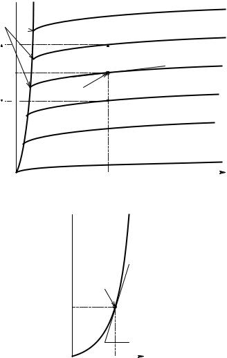
For a silicon BJT with IBQ = 5 ∞ 10−5 A, rπ = 1.04 kΩ.
Figure 2.14 illustrates how the four C–E h-parameters vary with IC/ICQ at constant VCEQ. Note that the forward current gain, hfe, is the most constant with IC/ICQ. The collector–emitter Norton conductance, hoe, increases monotonically with IC/ICQ because, as IC increases, the IC = f (VCE, IB) curves tip upward. hie decreases monotonically with increasing IC, as predicted by Equation 2.18. All four hxe parameters increase with temperature.
Another MFSSM used to analyze transistor amplifier behavior on paper is the grounded-base, h-parameter model, shown in Figure 2.15. Clearly, this MFSSM is useful in analyzing grounded-base BJT amplifiers; however, the same results can be obtained using the more common grounded-emitter, h-parameter MFSSM. The GB h-parameters are found experimentally from:
hib |
= |
vEB |
|
|
|
ohms |
(2.19A) |
|
iE |
|
|
|
|||||
|
|
|
Q, vCB = const. |
|
||||
|
|
|
|
|||||
|
|
|
|
|
|
|
||
|
hrb = |
|
|
vEB |
|
|
(2.19B) |
|
|
|
|
iCB |
|
Q,ie = const. |
|||
|
|
|
|
|
|
|
||
© 2004 by CRC Press LLC
40 |
Analysis and Application of Analog Electronic Circuits |
|||
ie E |
hib |
|
|
C ic |
|
+ |
hfbie |
|
+ |
|
|
|
|
|
|
hrbvcb |
|
hob |
vcb |
|
− |
|
|
− |
|
|
|
|
|
B |
|
|
B |
|
FIGURE 2.15
The common-base h-parameter SSM for npn and pnp BJTs. Using linear algebra, it is possible to express any set of four linear, two-port parameters in terms of any others. (Northrop, R.B., 1990, Analog Electronic Circuits: Analysis and Applications, Addison–Wesley, Reading, MA.)
|
hfb |
= |
|
|
iC |
|
|
(2.19C) |
|
|
|
|
iE |
|
Q, vCB = const. |
||||
|
= |
|
iC |
|
|
|
|
||
hob |
|
|
|
|
|
siemens |
(2.19D) |
||
|
|
|
|
|
|||||
vCB |
|
|
|
||||||
|
|
|
Q,iE = const. |
|
|||||
|
|
|
|||||||
Most manufacturers of discrete BJTs do not give GB h-parameters in their specification data sheets.
2.3.3Amplifiers Using One BJT
Three basic amplifier configurations can be made with one BJT: (1) the grounded-emitter; (2) the emitter-follower (grounded collector); and (3) the grounded-base amplifier. These three configurations are described and analyzed next.
The first example illustrates how to use the C–E h-parameter MFSSM to find expressions for the voltage gain, KV, and the input and output resistance of a grounded emitter amplifier, shown in Figure 2.16(A). This figure illustrates a basic grounded emitter amplifier driven by a small ac signal, vs, through a coupling capacitor, Cc. In the MFSSM amplifier model, only smallsignal variations around the BJT’s operating (Q) point are considered; thus all dc voltage sources are set to zero and replaced with short circuits to ground. Figure 2.16(B) illustrates the complete amplifier model (hre = 0 for simplicity). The SS output voltage is, by inspection:
vo |
= |
−hfeib |
(2.20) |
||
Gc |
+ hoe |
||||
|
|
|
|||
The base current is given by Ohm’s law, assuming negligible SS current flows in RB (RB hie).
© 2004 by CRC Press LLC
Models for Semiconductor Devices Used in Analog Electronic Systems |
41 |
|||
|
|
VCC |
|
|
IBQ |
|
|
|
|
|
RB |
RC |
|
|
|
vo |
|
|
|
|
|
|
|
|
Rs |
|
Rs |
vb B hie |
C vo |
|
|
Cc |
|
|
Cc |
|
npn BJT |
hfe ib |
|
|
|
|
||
|
|
|
ib |
|
vs |
|
vs |
RB |
hoe GC |
|
|
|
E |
|
A |
|
|
B |
|
FIGURE 2.16
(A) Schematic of a simple, capacitively coupled, grounded-emitter BJT amplifier. (B) Linear, mid-frequency, small-signal model (MFSSM) of the grounded-emitter amplifier. Note that, at mid-frequencies, capacitors are treated as short circuits and DC source voltages are small-signal grounds. The mid-frequency gain, vo /vs, can be found from the model; see text.
ib |
|
|
vs |
(2.21) |
|
Rs |
+ hie |
||||
|
|
|
Thus, the amplifier’s SS voltage gain is found by substituting Equation 2.21 into Equation 2.20:
vo |
= |
−hfeRC |
= K |
|
(2.22) |
|
vs |
(hoeRC + 1)(Rs + hie ) |
V |
||||
|
|
|
||||
|
|
|
|
By inspection, its SS input resistance is Rin Rs + hie and its (Thevenin)
output resistance is Rout = 1/(hoe + GC).
In a second example, a BJT emitter-follower amplifier is shown in Figure 2.17. Figure 2.17(B) illustrates the MFSSM for the emitter follower. To find an expression for the EF gain, write the node equations for the vb and vo nodes:
vb [Gs + GB + gie] − vo [gie] = vs Gs |
(2.23A) |
−vb gie + vo [GE + hoe + gie] − hfe ib = 0 |
(2.23B) |
where gie = 1/hie and ib = (vb − vo)gie. When the expression for ib is substituted into Equation 2.23B,
−vb[gie (1+ hfe )]+ vo[GE + hoe + gie (1+ hfe )]= 0 |
(2.24) |
© 2004 by CRC Press LLC
42 |
Analysis and Application of Analog Electronic Circuits |
VCC |
|
|
|
|
|
npn BJT |
Rs |
vb |
hie |
C |
|
RB |
|
|
B |
|
hfe ib |
Cc |
|
|
|
ib |
|
|
vs |
RB |
|
hoe |
|
Rs |
|
|
|||
Cc |
vo |
|
|
|
E |
|
|
|
|
vo |
|
|
|
|
|
|
|
vs |
|
|
|
|
|
RE |
|
|
|
RE |
(hfe + 1)ib |
A |
|
B |
|
|
|
FIGURE 2.17
(A) Schematic of a simple, capacitively coupled, emitter-follower amplifier. (B) MFSSM of the EF amplifier.
Now Equation 2.23A and Equation 2.24 are solved using Cramer’s rule, yielding the voltage gain:
vo |
= |
|
Gs gie (1+ hfe ) |
|
|
= K |
|
(2.25) |
|
[ |
|
] |
|
V |
|||
vs |
|
(Gs + GB ) GE + hoe + gie (1+ hfe ) |
+ gie (GE + hoe ) |
|
|
|||
|
|
|
|
|||||
This rather unwieldy expression can be simplified using the a priori knowledge that, usually, GE hoe and Gs GB. Equation 2.25 is multiplied top and bottom by hie RE Rs. After some algebra, the simplified EF gain is found to be:
KV |
|
|
RE (1+ hfe ) |
|
(2.26) |
RE (1 |
+ hfe )+ hie |
|
|||
|
|
+ Rs |
|||
Note that Kv for the EF is positive (noninverting) and slightly less than 1. What then is the point of an amplifier with no gain? The answer lies in the EF’s high input impedance and low output impedance. The EF is used to buffer sources and drive coaxial cables and transmission lines with low characteristic impedances. It is easy to show that the EF’s input impedance
at the vb node is simply RB in parallel with [hie + RE (1 + hfe)] (hoe is neglected). The Thevenin output impedance can be found for the linear MFSSM by
taking the ratio of the open circuit voltage (OCV) to its short-circuit current (SCC). The OCV is simply vs KV:
|
|
vsRE (1+ hfe ) |
|||
VOC |
|
|
|
(2.27) |
|
RE (1 |
+ hfe )+ hie |
|
|||
|
|
+ Rs |
|||
© 2004 by CRC Press LLC
Models for Semiconductor Devices Used in Analog Electronic Systems |
43 |
||||
|
−VCC |
|
|
|
|
|
|
|
|
hoe |
|
|
IBQ |
RC |
|
hfe ib |
|
|
|
|
|
|
|
|
Rs |
vo |
Rs ve |
|
vo |
|
|
|
E |
C |
|
|
|
|
|
|
|
|
|
|
|
ib |
|
vs |
RB |
|
vs |
|
RC |
|
|
|
|
B |
|
|
|
|
|
hie |
|
|
Cb |
|
|
|
|
|
A |
|
B |
|
|
FIGURE 2.18
(A) Schematic of a simple, capacitively coupled, grounded-base amplifier. (B) MFSSM of the GB amplifier.
The SCC is simply ibsc(1 + hfe). When the output is short-circuited, vo = 0 and ibsc = vs/(Rs + hie). Thus, Rout is:
|
|
vsRE (1+ hfe ) |
||
R = |
|
RE (1+ hfe )+ hie + Rs |
||
|
|
vs (1 |
+ hfe ) |
|
out |
|
|||
|
|
|
||
|
|
|
(Rs |
+ hie ) |
|
|
|
(Rs + hie ) |
|
|
|
= |
|
RE |
(1+ hfe ) |
|
(2.28) |
|
|
(Rs |
+ hie ) |
+ R |
|||
|
|
(1+ hfe ) |
E |
|
||
|
|
|
|
|||
Equation 2.28 shows that Rout is basically RE in parallel with (Rs + hie)/(1 + hfe).
In general, Rout will be on the order of 10 to 30 Ω.
The third single BJT circuit of interest is the grounded-base amplifier, shown in Figure 2.18. Again, to find the GB amp’s gain, the node equations are written on the ve and vo nodes:
ve [Gs + gie + hoe] − vo hoe − hfe ib = vs Gs |
(2.29A) |
−ve hoe + vo [hoe + GC] + hfe ib = 0 |
(2.29B) |
Now ib = −ve gie is substituted into the preceding equations to get the final form for the node equations:
ve[Gs + hoe + gie (1+ hfe )]− vo[hoe ] = vsGs |
(2.30A) |
−ve[hoe + hfe gie ]+ vo[hoe + GC ]= 0 |
(2.30B) |
© 2004 by CRC Press LLC

44 |
Analysis and Application of Analog Electronic Circuits |
These equations are solved using Cramer’s rule. After some algebra, the GB amplifier gain is obtained:
Kv |
= |
|
RC[hfe |
+ hoehie ] |
(2.31) |
|
RC[hoe (hie |
+ Rs )]+ Rs[1+ hfe + hoehie ]+ hie |
|||||
|
|
|
||||
It is instructive to substitute typical numerical values into Equation 2.31
and evaluate the gain. Let RC = 5 k; hie = 1 k; hfe = 100; Rs = 100; and hoe = 10− 5 S. Kv = 44.8. Note that the gain is noninverting. From the numerical eval-
uation, certain terms in Equation 2.31 are found to be small compared with others (i.e., hoe 0), which leads to the approximation:
Kv |
|
|
RChfe |
(2.32) |
|
Rs (1 |
+ hfe )+ hie |
||||
|
|
|
Next an expression will be found for and Rin and Rout evaluated for the GB amplifier. Rin is the resistance the Thevenin source (vs, Rs) “sees” looking into
the emitter of the GB amplifier. Assume hoe 0. The resistance looking into the emitter is approximately:
R |
ve |
− |
ve |
= |
ve |
= |
hie |
(2.33) |
|
−ib (hfe + 1) |
−(−ve hie )(hfe + 1) |
(hfe + 1) |
|||||
inem |
ie |
|
|
|
||||
|
|
|
|
|||||
To get a feeling for the size of Rin, substitute realistic circuit parameter
values. Let RC = 5000 Ω; Rs = 100 Ω; hfe = 100; hoe = 10−5 S; and hie = 1000 Ω. Thus, Rinem = 9.9 Ω. The output resistance is the Thevenin resistance seen
looking into the collector node with RC attached. If hoe 0 is set again, Rout RC, by inspection.
2.3.4Simple Amplifiers Using Two Transistors at Mid-Frequencies
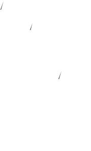
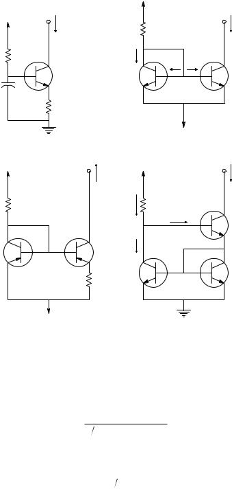
Figure 2.19 illustrates four common two-BJT amplifier architectures. An npn Darlington pair is shown in Figure 2.19(A). Darlington pairs can also use pnp BJTs. These pairs are often used as power amplifiers in the emitterfollower architecture or as grounded-base amplifiers. Figure 2.19(B) is called a feedback pair; it is not a Darlington. It, too, is often used as a power amplifier in the EF or GE modes and will be analyzed later. Figure 2.19(C) is an EF–GB pair, used for small-signal, high-frequency amplification. Figure 2.19(D) is called a cascode pair; it is also used as a small-signal, high-frequency amplifier.
In the first example, an expression for the mid-frequency, small-signal voltage gain, as well as input and output resistances for a grounded-emitter Darlington amplifier, are found. The amplifier circuit and its MFSS CE
© 2004 by CRC Press LLC
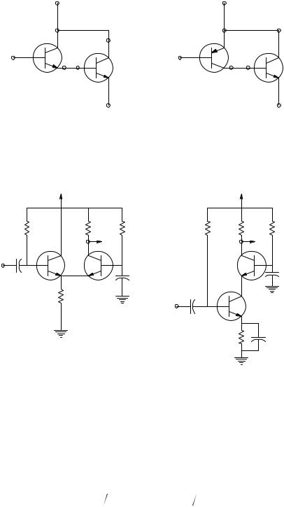
Models for Semiconductor Devices Used in Analog Electronic Systems |
45 |
|
C1 |
E1 |
C2 |
Q1 |
C2 |
Q1 |
|
|
|
||
B1 |
Q2 |
B1 |
Q2 |
|
|||
|
E1 B2 |
C1 |
B2 |
A E2 B E2
|
VCC |
|
|
|
VCC |
|
RB |
|
RC |
RB |
RB |
RC |
RB |
|
|
|
vo |
|
vo |
|
|
Q1 |
|
Q2 |
|
|
|
|
|
|
|
|
|
|
vs |
|
|
|
|
Q2 |
|
|
|
|
|
|
|
|
|
|
|
|
Q1 |
|
|
|
RE |
C |
|
vs |
D |
|
|
|
|
|
|||
|
|
|
|
|
||
|
|
|
|
|
RE |
|
FIGURE 2.19
Four common two-BJT amplifier configurations: (A) The Darlington pair. Note that Q1’s emitter is connected directly to Q2’s base. (B) The feedback pair. The collector of the pnp Q1 is coupled directly to the npn Q2’s base. (C) The emitter-follower–grounded-base (EF–GB) BJT pair. (D) The cascode pair.
h-parameter model are shown in Figure 2.20. To simplify analysis, assume
RB •, hoe1 0, and hoe2 0. From Ohm’s law, ib1 = (vs – vb2)/(Rs + hie1),
ib2 = vb2/hie2.
Now write node equations for the vb2 and the vo nodes:
vb2 [1 hie2 + 1 (Rs + hie1)]− hfe1ib1 = vs (Rs + hie1) |
(2.34A) |
© 2004 by CRC Press LLC
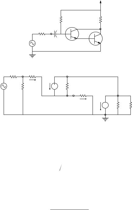
46 |
Analysis and Application of Analog Electronic Circuits |
VCC
RB |
RC |
|
Q1 |
Rs |
vo |
|
|
vs |
Q2 |
|
Rs |
vb1 hie1 |
C1 |
|
ib1 |
hfe1ib1 |
|
|
|
vs |
RB |
hoe1 |
|
vb2 hie2 |
C2 vo |
|
E1 |
B2 |
ib2 |
hfe2ib2 |
|
|
|
|
hoe2 RC
FIGURE 2.20
Top: a common-emitter Darlington amplifier. Bottom: C–E h-parameter MFSSM of the Darlington amplifier. Analysis is in the text.
|
|
vo [GC] + hfe1ib1 + hfe2ib2 = 0 |
|
|
(2.34B) |
and then substitute the relations for ib1 and ib2 and find: |
|
|
|||
vo |
|
+ (1+ hfe1) (Rs + hie1) = vs[(1+ hfe1) |
(Rs |
˘ |
(2.35A) |
[0] + vb2 1 hie2 |
+ hie1)]˙ |
||||
|
|
|
|
˚ |
|
|
vo[GC ] + vb2[hfe2 hie2 − hfe1 (Rs + hie1)]= −vshfe1 |
(Rs + hie1) |
(2.35B) |
||
Using Cramer’s rule, find the GE Darlington amplifier’s voltage gain:
vo |
|
RC (1+ hfe1 + hfe1hfe2 ) |
|
|
|
− |
(Rs + hie1)+ hie2 (1+ hfe1) |
= Kv |
(2.36) |
vs |
||||
© 2004 by CRC Press LLC
Models for Semiconductor Devices Used in Analog Electronic Systems |
47 |
VCC
RB RC
Q1 vo
Rs |
Q2 |
vs
E1
|
hoe1 |
|
|
|
hfe1ib1 |
vb2 |
hie2 |
C2 |
vo |
Rs B1 hie1 |
||||
C1 |
B2 |
ib2 |
hfe2ib2 |
|
ib1 |
|
|
|
|
vs |
|
|
hoe2 |
GC |
E2
FIGURE 2.21
Top: feedback pair amplifier with load resistor, RC, attached to common Q1 emitter + Q2 collector. Bottom: MFSSM of the feedback pair amplifier above. Analysis in text shows this circuit behaves like a super emitter follower.
By inspection, the Thevenin Rout RC and Rin hie1 + (1 + hfe1)hie2. As the section on BJT amplifier frequency response demonstrates, the GE Darlington
has relatively poor high-frequency response, trading off gain for bandwidth. This example considers the feedback pair amplifier shown in Figure 2.19(B) and Figure 2.21. Note that in this amplifier, it is the collector of the pnp Q1 that drives the base of the npn Q2, and Q2’s collector is tied to Q1’s emitter.
The auxiliary equations are: |
|
ib1 = (vs – vo)/(Rs + hie1) |
(2.37A) |
ib2 = vb2/hie2 |
(2.37B) |
© 2004 by CRC Press LLC
48 Analysis and Application of Analog Electronic Circuits
Again, for mathematical convenience, use the approximations hoe1 0 and |
||
hoe2 0, and write the node equations for vo and vb2: |
|
|
vo[GC + 1 (Rs + hie |
1)]+ hfe2ib2 − hfe1ib1 = vs (Rs + hie1) |
(2.38A) |
vb2 |
[1 hie1]+ hfe1 ib1 = 0 |
(2.38B) |
Now substitute the auxiliary relations for ib1 and ib2 into Equations 2.38A
and Equation 2.38B: |
|
|
|
|
|
|
|
|
+ |
1+ hfe1 |
˘ |
+ vb2[hfe2 |
hie2 ]= vs |
1+ hfe1 |
|
vo GC |
|
˙ |
|
(2.39A) |
|||
R + h |
R + h |
||||||
|
|
s ie1 |
˚ |
|
|
s ie1 |
|
−vo |
hfe1 |
+ vb2[1 hie2 ]= − |
vs |
(2.39B) |
R + h |
R + h |
|||
|
s ie1 |
|
s ie1 |
|
The two preceding equations are solved by Cramer’s rule to find Kv.
|
|
|
1+ h |
fe1 |
˘ |
|
|
h |
fe1 |
h |
fe2 |
|||
= (1 hie1) GC |
+ |
|
˙ |
+ |
|
|
|
|||||||
|
|
hie2 |
(Rs + hie1) |
|||||||||||
|
|
|
Rs + hie1 ˚ |
|
||||||||||
v |
|
= |
(1+ hfe1)hie2 + hfe2hie1 |
|
|
|
||||||||
|
o |
|
|
hie1hie2 (Rs + hie1) |
|
|
|
|
|
|||||
|
|
|
|
|
|
|
|
|
||||||
Thus, the voltage gain is:
vo |
|
|
RC |
(1+ hfe1 + hfe |
2hfe1) |
|
|
|
|
[ |
|
] |
= K |
|
|
|
[ |
|
] |
|
v |
||
vs |
|
RC (1+ hfe1 + hfe1hfe2 ) |
+ (Rs + hie1) |
|
|||
|
|
|
|||||
(2.40)
(2.41)
(2.42)
Taking “typical” numerical values, Rs + hie1 = 1050 Ω; hfe1 = 100; hfe2 = 20; and RC = 5000 Ω, then Kv = 0.999895. It appears that the feedback pair amplifier of Figure 2.21 behaves like a super emitter follower with (almost) unity gain.
Next, examine Rin and Rout of the FBP amplifier. To find Rout, use the opencircuit voltage/short-circuit current method. The OCV approximated by
vs voc because of the near unity gain of the amplifier. The short-circuit current at the C2–E1 node is:
isc = (1 + hfe1) ib1 − hfe2 ib2 |
(2.43) |
With the output short-circuited, vo = 0 and ib1 = vs/(Rs + hie1). Neglecting hoe1, it is possible to write:
© 2004 by CRC Press LLC

Models for Semiconductor Devices Used in Analog Electronic Systems
ib2 = −hfe1 ib1 = −hfe1 vs/(Rs + hie1)
Thus:
isc = (1 + hfe1)vs/(Rs + hie1) + hfe2 hfe1 vs/(Rs + hie1)
Clearly, Rout = voc/isc, yielding:
Rout |
|
|
Rs + hie1 |
|
+ hfe1 + hfe1hfe2 |
||
|
1 |
||
49
(2.44)
(2.45)
(2.46)
If the numbers used previously are substituted, Rout = 0.5 Ω — significantly smaller than a single BJT’s emitter follower. Rin looking into the B1 node is just vs/ib1. That is:
Rin = vshie1 (vs − vo ) = hie1 |
(1− vo |
vs ) = |
|
hie1 |
|
|
1− |
RC[1+ hfe1 + hfe1hfe2 ] |
|||||
|
|
|
||||
¬ |
|
|
RC[1+ hfe1 + hfe1hfe2 ]+ hie1 |
|
||
|
|
|
(2.47) |
|||
Rin = RC[1+ hfe1 + hfe1hfe2 ] |
+ hie1 |
|
|
|||
|
|
|
|
|||
Rin 10.51 MΩ, using the previous parameters.
Next, examine the behavior of the feedback pair when the load resistor is connected to E2 and C2–E1 is connected to Vcc. The circuit is shown in Figure
2.22. It is not necessary to solve two simultaneous node equations to find Kv; by Ohm’s law, ib1 = vs/(Rs + hie1) and ib2 = −ib1hfe1. Now it is clear that:
vo |
= ib2 (1+ hfe2 )RE |
= −ib1hfe1 |
(1+ hfe2 )RE = |
−vshfe1(1+ hfe2 )RE |
= voOC |
(2.48) |
||||
|
|
|||||||||
|
|
|
|
|
|
|
|
Rs + hie1 |
|
|
Thus, |
|
|
|
|
|
|
|
|
|
|
|
|
K |
|
= − |
REhfe1(1+ hfe2 ) |
|
(2.49) |
|||
|
|
v |
(Rs + hie1) |
|||||||
|
|
|
|
|
|
|||||
|
|
|
|
|
|
|
||||
Rin for this amplifier is found by inspection; Rin = hie1. Rout is found by voOC/ioSC:
|
|
−vshfe1(1+ hfe2 )RE |
|
|
|
Rout |
= |
(Rs |
+ hie1) |
= RE |
(2.50) |
−vshfe1(1+ hfe2 ) |
|||||
|
|
(Rs |
+ hie1) |
|
|
© 2004 by CRC Press LLC
50 |
Analysis and Application of Analog Electronic Circuits |
VCC
RB
Q1
Rs |
Cc |
Q2 |
vs
+
RE vo
Rs B1 hie1 |
C1 vb2 hie2 |
C2 |
|
hfe1ib1 |
B2 |
ib2 |
hfe2ib2 |
ib1 |
|
|
|
vs |
hoe1 |
|
hoe2 |
|
|
|
E2 |
E1 vo
RE
FIGURE 2.22
Top: feedback pair amplifier with load resistor in Q2’s emitter. Bottom: MFSSM of the amplifier shown above. Analysis in text shows this amplifier has a high inverting mid-frequency gain; it does not emulate an emitter follower.
Next, examine the gain, Rin and Rout, of the emitter-follower-grounded base amplifier shown in Figure 2.19(C). Figure 2.23 illustrates the MFSSM for this amplifier. Again, for algebraic simplicity, assume that hoe1 and hoe2 are negligible; also, R1 = Rs + hie1, all capacitors behave as short circuits at mid-frequencies, and RB •. Two node equations can be written for the MFSSM:
© 2004 by CRC Press LLC

Models for Semiconductor Devices Used in Analog Electronic Systems |
51 |
|
|
|
|
|
RE |
|
Rs |
B1 |
hie1 |
E1 |
E2 |
ve |
hie2 |
|
|
|
|
|
|
B2 |
|
|
ib1 |
|
|
|
|
vs |
|
|
hoe1 |
|
|
hoe2 |
|
|
|
|
|
||
|
|
hfe1ib1 |
|
hfe2 ib2 |
|
|
|
|
|
C1 |
|
C2 |
|
|
|
|
|
|
|
vo |
|
|
|
|
|
|
RC |
FIGURE 2.23
MFSSM for the EF–GB amplifier of Figure 2.19(C). See text for analysis.
vo [GC] + hfe2 ib2 = 0 |
(2.51A) |
ve [GE + 1/hie2 + G1] − hfe2 ib2 − hfe1ib1 = vs G1 |
(2.51B) |
where: |
|
ib2 = −ve/hie2 |
(2.51C) |
ib1 = (vs – ve)G1 |
(2.51D) |
Substituting Equation 2.51C and Equation 2.51D into the node equations yields:
vo [GC] − ve [hfe2/hie2] = 0 |
(2.52A) |
[ |
] |
G1(1+ hfe1) |
|
|
vo[0]+ ve GE |
+ (1+ hfe2 ) hie2 + G1(1+ hfe1) |
= vs |
(2.52B) |
|
From Equation 2.52A and Equation 2.52B, |
|
|
|
|
|
vo = ve RC [hfe2/hie2] |
|
|
(2.53) |
can be written and
ve = |
[ |
vsG1 |
(1 |
+ hfe1) |
] |
(2.54) |
+ (1+ hfe2 ) |
|
|
||||
GE |
hie2 + G1(1+ hfe1) |
|||||
© 2004 by CRC Press LLC
52 |
Analysis and Application of Analog Electronic Circuits |
||||
|
|
|
|
C2 |
vo |
|
|
|
hfe2ib2 |
|
|
|
|
|
|
hoe2 |
|
|
|
|
E2 |
|
|
Rs |
B1 |
ib1 |
ve |
|
|
C1 |
|
|
|||
|
|
|
hfe1ib1 |
hie2 |
RC |
|
|
|
ib2 |
|
|
vs |
|
hie1 |
hoe1 |
B2 |
|
|
|
|
E1 |
|
|
FIGURE 2.24
MFSSM for the cascode amplifier of Figure 2.19(D). See text for analysis.
Now Equation 2.54 is substituted into Equation 2.53 to find Kv:
K |
|
= |
vo |
= |
RChfe2 (1+ hfe1) |
|
(2.55) |
|
v |
vs |
hie2 (R1 RE )+ R1(1+ hfe2 )+ hie2 (1 |
+ hfe1) |
|||||
|
|
|
|
|||||
|
|
|
|
|
Substitute typical values RC = 5000 Ω; R1 = 1050 Ω; hfe1 = hfe2 = 100; and hie2 = 1000 Ω, and find Kv = +244, i.e., the EF–GB amplifier is noninverting. The EF–GB amplifier will be shown to have excellent high-frequency response. It is left as an exercise for the reader to find expressions for the mid-frequency Rin and Rout for this amplifier.
The final two-BJT amplifier stage to be analyzed using the CE MFSSM is the cascode amplifier, shown in Figure 2.19(D). The MFSSM for this amplifier is shown in Figure 2.24. Again, assume capacitors behave as short circuits
at mid-frequencies, hoe1 = hoe2 = 0, and RB •. Clearly, vo = −hfe2 ib2 RC and ib2 = −ve/hie2, so vo = ve hfe2 RC/hie2 and ib1 = vs/R1. To find ve, write the node equation:
ve [1/hie2] + hfe1ib1 − hfe2 ib2 = 0 |
(2.56) |
Substituting for ib1 and ib2 into Equation 2.56 yields:
ve |
= |
−vshfe1hie2G1 |
(2.57) |
||
1 |
+ hfe2 |
||||
|
|
|
|||
© 2004 by CRC Press LLC
Models for Semiconductor Devices Used in Analog Electronic Systems |
53 |
Equation 2.57 is substituted into the preceding equation for vo to find Kv:
K |
|
= |
vo |
= |
−hfe1RChfe2 |
♠ |
−hfe1RC |
(2.58) |
|
v |
vs |
R1(1+ hfe2 ) |
R1 |
||||||
|
|
|
|
|
|||||
|
|
|
|
|
|
By inspection, Rin = R1, Rout RC. Like the EF–GB amplifier, the cascode amplifier has a high-frequency bandwidth. It also can be described as a GE–GB amplifier.
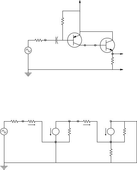
2.3.5The Use of Transistor Dynamic Loads To Improve Amplifier Performance
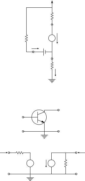
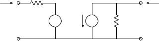
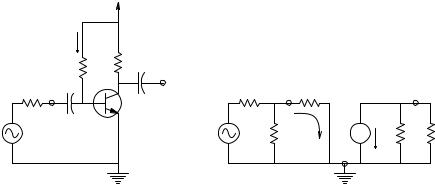
In many analog IC designs, including those with differential amplifiers, transistors and small transistor circuits are used to create small-signal, dynamic high impedances that, when used in amplifiers to replace conventional resistors, increase amplifier gain or differential amplifier common-mode rejection ratio. Figure 2.25 illustrates four BJT circuits that act as dc current sources or sinks with high, small-signal, Norton resistances. For example, if 2 mA dc flows through a potential difference of 5 V in an electronic circuit, a 2.5-k resistor is needed. If a dynamic current source is used, the equivalent small-signal (Norton) resistance can range from 100 k to 10 M, depending on the circuit. A good way to view such dynamic resistances is to treat the circuit as a dc current source in parallel with a Norton resistance of 100 k to 10 M.
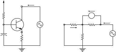
The most basic dynamic resistance is realized by looking into the collector of a BJT with an emitter resistance that is not bypassed, as shown in Figure 2.25(A). Figure 2.26 illustrates how the MFSSM is used to find the resistance looking into the collector. Note that the base is bypassed to ground at signal
frequencies. Clearly, from Ohm’s law, Rincol = vt/it. (vt is a small-signal test source.)
Begin analysis by finding an expression for ve = f (vt). Writing the node equation:
ve[(1 hie )+ GE + hoe ]− βib = vt hoe |
(2.59A) |
|
ib = −ve |
hie |
(2.59B) |
¬ |
|
|
ve[(1 hie )(1+ β) + Ge |
+ hoe ]= vt hoe |
(2.59C) |
© 2004 by CRC Press LLC
54 |
Analysis and Application of Analog Electronic Circuits |
||
|
VCC > 0 |
|
|
VBB > 0 |
|
|
|
IS |
|
|
IS |
|
RC |
|
|
RB |
IC1 |
IB1 |
IB2 |
|
|
||
|
Q1 |
+ |
Q2 |
|
|
|
|
|
|
VBE |
|
RE |
|
− |
|
|
|
|
|
B
A
VEE < 0
VCC < 0 |
|
|
VCC > 0 |
|
|
|
IS |
|
IS |
RC |
|
|
IRc |
RC |
|
|
|
|
IB3 |
|
|
|
|
Q3 |
Q1 |
|
Q2 |
IC1 |
|
|
+ |
|
|
|
|
VBE1 |
|
Q1 |
Q2 |
|
RE |
|
+ |
|
|
|
|
||
|
− |
|
|
VBE |
|
|
|
− |
|
|
|
|
|
|
C |
VEE > 0 |
|
D |
|
FIGURE 2.25
Four BJT circuits used for high-impedance current sources and sinks in the design of differential amplifiers and other analog ICs. They can serve as high-impedance active loads. (A) Collector of simple BJT with unbypassed emitter resistance. (B) Basic two-BJT current sink. (C) Widlar current source (pnp BJTs are used). (D) Wilson current sink.
Thus, ve is:
ve = |
vthoe |
(2.60) |
(1 hie )(1+ β) + GE + hoe |
||
and the test current is: |
|
|
it = ve[(1 hie )+ GE ] |
(2.61) |
|
© 2004 by CRC Press LLC
Models for Semiconductor Devices Used in Analog Electronic Systems |
55 |
|||
VBB |
|
|
|
|
it |
|
|
|
|
|
|
|
β ib |
|
RB |
|
|
|
|
+ |
B |
hie ve |
hoe |
it |
|
|
|||
vt |
|
|
|
|
|
|
E |
C |
+ |
Cb |
|
ib |
|
|
|
|
|
|
vt |
RE |
|
RE |
|
|
|
|
|
|
|
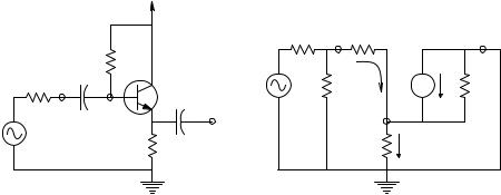
FIGURE 2.26
Left: test circuit for calculating small-signal resistance looking into BJT’s collector. An ac test source, vt, is used; it is measured. Right: MFSSM of the test circuit used to calculate the expression for the small-signal resistance looking into collector.
When Equation 2.60 is substituted into Equation 2.61, it is possible to solve
for Rincol:
|
|
|
1+ |
β RE + hoehieRE |
|
|
R = |
vt |
= |
RE |
+ hie |
|
|
|
(2.62) |
|||||
|
|
|
|
|||
incol |
it |
|
|
hoe |
|
|
|
|
|
|
|
||
Looking into the collector of a BJT with no RE, Rincol hoe−1 Ω can be seen. To see how much RE increases Rincol, substitute some typical parameter values
into Equation 2.62: RE = 5k; hie = 1k; β = 100; and hoe = 10−5 S. Crunching the
numbers, Rincol = 8.4 MΩ. Note that the BJT’s base was bypassed to ground in the preceding development. If the base is not bypassed, hie hie + RB in
Equation 2.62, where RB is the Thevenin resistance that the base “sees.” The
unbypassed base causes Rincol to decrease markedly, but it still remains above 1/hoe.
More sophisticated, high dynamic resistance dc current sources are shown in Figure 2.25(B) and Figure 2.25(C). Figure 2.25(B) is the basic, two-BJT current sink; its dynamic input resistance is about 1/hoe Ω. Figure 2.25(C) is the Widlar current source (note pnp BJTs are used). Figure 2.25(D) is a Wilson current sink. Note that a collector–base junction in all three current source/active load circuits is short-circuited (Q1 in Figure 2.25(B) and Figure 2.25(C), Q2 in Figure 2.25(D)). The transistor with the shorted collector–base junction then behaves as a forward-biased, base–emitter diode junction.
Analysis of the basic two-BJT current sink (Figure 2.25(B)) is made easy when it is assumed that Q1 and Q2 have identical parameters. Because both transistors have the same VBE, their collector currents are equal, i.e., IC1 = IC2. Summing currents at Q1’s collector,
IRc − IC1 = 2IC1/β |
(2.63) |
© 2004 by CRC Press LLC