

- •Analysis and Application of Analog Electronic Circuits to Biomedical Instrumentation
- •Dedication
- •Preface
- •Reader Background
- •Rationale
- •Description of the Chapters
- •Features
- •The Author
- •Table of Contents
- •1.1 Introduction
- •1.2 Sources of Endogenous Bioelectric Signals
- •1.3 Nerve Action Potentials
- •1.4 Muscle Action Potentials
- •1.4.1 Introduction
- •1.4.2 The Origin of EMGs
- •1.5 The Electrocardiogram
- •1.5.1 Introduction
- •1.6 Other Biopotentials
- •1.6.1 Introduction
- •1.6.2 EEGs
- •1.6.3 Other Body Surface Potentials
- •1.7 Discussion
- •1.8 Electrical Properties of Bioelectrodes
- •1.9 Exogenous Bioelectric Signals
- •1.10 Chapter Summary
- •2.1 Introduction
- •2.2.1 Introduction
- •2.2.4 Schottky Diodes
- •2.3.1 Introduction
- •2.4.1 Introduction
- •2.5.1 Introduction
- •2.5.5 Broadbanding Strategies
- •2.6 Photons, Photodiodes, Photoconductors, LEDs, and Laser Diodes
- •2.6.1 Introduction
- •2.6.2 PIN Photodiodes
- •2.6.3 Avalanche Photodiodes
- •2.6.4 Signal Conditioning Circuits for Photodiodes
- •2.6.5 Photoconductors
- •2.6.6 LEDs
- •2.6.7 Laser Diodes
- •2.7 Chapter Summary
- •Home Problems
- •3.1 Introduction
- •3.2 DA Circuit Architecture
- •3.4 CM and DM Gain of Simple DA Stages at High Frequencies
- •3.4.1 Introduction
- •3.5 Input Resistance of Simple Transistor DAs
- •3.7 How Op Amps Can Be Used To Make DAs for Medical Applications
- •3.7.1 Introduction
- •3.8 Chapter Summary
- •Home Problems
- •4.1 Introduction
- •4.3 Some Effects of Negative Voltage Feedback
- •4.3.1 Reduction of Output Resistance
- •4.3.2 Reduction of Total Harmonic Distortion
- •4.3.4 Decrease in Gain Sensitivity
- •4.4 Effects of Negative Current Feedback
- •4.5 Positive Voltage Feedback
- •4.5.1 Introduction
- •4.6 Chapter Summary
- •Home Problems
- •5.1 Introduction
- •5.2.1 Introduction
- •5.2.2 Bode Plots
- •5.5.1 Introduction
- •5.5.3 The Wien Bridge Oscillator
- •5.6 Chapter Summary
- •Home Problems
- •6.1 Ideal Op Amps
- •6.1.1 Introduction
- •6.1.2 Properties of Ideal OP Amps
- •6.1.3 Some Examples of OP Amp Circuits Analyzed Using IOAs
- •6.2 Practical Op Amps
- •6.2.1 Introduction
- •6.2.2 Functional Categories of Real Op Amps
- •6.3.1 The GBWP of an Inverting Summer
- •6.4.3 Limitations of CFOAs
- •6.5 Voltage Comparators
- •6.5.1 Introduction
- •6.5.2. Applications of Voltage Comparators
- •6.5.3 Discussion
- •6.6 Some Applications of Op Amps in Biomedicine
- •6.6.1 Introduction
- •6.6.2 Analog Integrators and Differentiators
- •6.7 Chapter Summary
- •Home Problems
- •7.1 Introduction
- •7.2 Types of Analog Active Filters
- •7.2.1 Introduction
- •7.2.3 Biquad Active Filters
- •7.2.4 Generalized Impedance Converter AFs
- •7.3 Electronically Tunable AFs
- •7.3.1 Introduction
- •7.3.3 Use of Digitally Controlled Potentiometers To Tune a Sallen and Key LPF
- •7.5 Chapter Summary
- •7.5.1 Active Filters
- •7.5.2 Choice of AF Components
- •Home Problems
- •8.1 Introduction
- •8.2 Instrumentation Amps
- •8.3 Medical Isolation Amps
- •8.3.1 Introduction
- •8.3.3 A Prototype Magnetic IsoA
- •8.4.1 Introduction
- •8.6 Chapter Summary
- •9.1 Introduction
- •9.2 Descriptors of Random Noise in Biomedical Measurement Systems
- •9.2.1 Introduction
- •9.2.2 The Probability Density Function
- •9.2.3 The Power Density Spectrum
- •9.2.4 Sources of Random Noise in Signal Conditioning Systems
- •9.2.4.1 Noise from Resistors
- •9.2.4.3 Noise in JFETs
- •9.2.4.4 Noise in BJTs
- •9.3 Propagation of Noise through LTI Filters
- •9.4.2 Spot Noise Factor and Figure
- •9.5.1 Introduction
- •9.6.1 Introduction
- •9.7 Effect of Feedback on Noise
- •9.7.1 Introduction
- •9.8.1 Introduction
- •9.8.2 Calculation of the Minimum Resolvable AC Input Voltage to a Noisy Op Amp
- •9.8.5.1 Introduction
- •9.8.5.2 Bridge Sensitivity Calculations
- •9.8.7.1 Introduction
- •9.8.7.2 Analysis of SNR Improvement by Averaging
- •9.8.7.3 Discussion
- •9.10.1 Introduction
- •9.11 Chapter Summary
- •Home Problems
- •10.1 Introduction
- •10.2 Aliasing and the Sampling Theorem
- •10.2.1 Introduction
- •10.2.2 The Sampling Theorem
- •10.3 Digital-to-Analog Converters (DACs)
- •10.3.1 Introduction
- •10.3.2 DAC Designs
- •10.3.3 Static and Dynamic Characteristics of DACs
- •10.4 Hold Circuits
- •10.5 Analog-to-Digital Converters (ADCs)
- •10.5.1 Introduction
- •10.5.2 The Tracking (Servo) ADC
- •10.5.3 The Successive Approximation ADC
- •10.5.4 Integrating Converters
- •10.5.5 Flash Converters
- •10.6 Quantization Noise
- •10.7 Chapter Summary
- •Home Problems
- •11.1 Introduction
- •11.2 Modulation of a Sinusoidal Carrier Viewed in the Frequency Domain
- •11.3 Implementation of AM
- •11.3.1 Introduction
- •11.3.2 Some Amplitude Modulation Circuits
- •11.4 Generation of Phase and Frequency Modulation
- •11.4.1 Introduction
- •11.4.3 Integral Pulse Frequency Modulation as a Means of Frequency Modulation
- •11.5 Demodulation of Modulated Sinusoidal Carriers
- •11.5.1 Introduction
- •11.5.2 Detection of AM
- •11.5.3 Detection of FM Signals
- •11.5.4 Demodulation of DSBSCM Signals
- •11.6 Modulation and Demodulation of Digital Carriers
- •11.6.1 Introduction
- •11.6.2 Delta Modulation
- •11.7 Chapter Summary
- •Home Problems
- •12.1 Introduction
- •12.2.1 Introduction
- •12.2.2 The Analog Multiplier/LPF PSR
- •12.2.3 The Switched Op Amp PSR
- •12.2.4 The Chopper PSR
- •12.2.5 The Balanced Diode Bridge PSR
- •12.3 Phase Detectors
- •12.3.1 Introduction
- •12.3.2 The Analog Multiplier Phase Detector
- •12.3.3 Digital Phase Detectors
- •12.4 Voltage and Current-Controlled Oscillators
- •12.4.1 Introduction
- •12.4.2 An Analog VCO
- •12.4.3 Switched Integrating Capacitor VCOs
- •12.4.6 Summary
- •12.5 Phase-Locked Loops
- •12.5.1 Introduction
- •12.5.2 PLL Components
- •12.5.3 PLL Applications in Biomedicine
- •12.5.4 Discussion
- •12.6 True RMS Converters
- •12.6.1 Introduction
- •12.6.2 True RMS Circuits
- •12.7 IC Thermometers
- •12.7.1 Introduction
- •12.7.2 IC Temperature Transducers
- •12.8 Instrumentation Systems
- •12.8.1 Introduction
- •12.8.5 Respiratory Acoustic Impedance Measurement System
- •12.9 Chapter Summary
- •References
Modulation and Demodulation of Biomedical Signals |
441 |
xm |
|
0 |
|
−xm |
|
Secondary |
+ |
coils |
|
Vc |
Vo |
−
Moving |
|
|
magnetic |
Vo |
|
core |
||
(rms) |
||
|
− x (mm) xm
xm
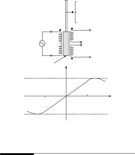
FIGURE 11.6
Top: cross-sectional schematic of an LVDT. The output is a DSBSC modulated carrier. Bottom: transfer curve of the RMS voltage output of the LVDT vs. core position. A 180∞ phase shift in the output is signified by Vo(x) < 0.
11.4 Generation of Phase and Frequency Modulation
11.4.1Introduction
Phase and frequency modulation are subsets of angle modulation, which has the general form:
ym(t) = A cos[ωct + Φ(t)] |
(11.19) |
The phase argument of the modulated carrier is [ωct + Φ(t)] radians and the frequency of the modulated carrier is [ωc + Φ° ] r/s. When Φ(t) = Kf mt (t) dt, FM is obtained; when Φ(t) = Kp m(t), PhM is the result. Many practical angle modulation and demodulation circuits have been developed since Edwin H.
© 2004 by CRC Press LLC
442 |
|
Analysis and Application of Analog Electronic Circuits |
|||||||||||||
|
|
|
|
|
|
(Loop |
|
|
|
|
|
||||
|
(PhD) |
|
|
|
filter) |
|
|
|
|
|
|||||
θi |
|
|
KP |
|
Kf (s + a) |
|
VL |
|
|||||||
vc(t) ωc |
− |
|
|
|
s |
|
|
|
|
|
|||||
|
|
|
|
|
|
|
|
|
|||||||
|
|
|
|
|
|
|
|
|
|
|
|
|
|
||
(XO) |
θo, ωc |
PLL |
|
(VCO) |
|
|
|
|
|
||||||
|
|
|
|
|
|
|
|
|
|||||||
|
|
|
|
|
|
|
Kv |
|
Vc |
|
|
|
vm(t) |
||
|
|
|
|
|
|
|
|
||||||||
|
|
|
|
|
|
|
|
|
|
|
|
|
|
|
|
|
|
|
|
|
|
|
s |
|
|
|
|
|
ωm |
||
|
|
|
|
|
|
|
|
|
|
|
|
|
|
|
|
Vo  (NBFM out)
FIGURE 11.7
Block diagram of a phase-locked loop used to generate narrowband FM.
Armstrong invented frequency modulation in 1933. Like many innovations in technology, FM did not “catch on” at once; it did not become widely used commercially until after World War II (Stark et al., 1988). A useful practical source of PhM and FM circuits can be found in the ARRL’s Radio Amateur’s Handbook, 1953.
11.4.2NBFM Generation by Phase-Locked Loop
Figure 11.7 illustrates at the systems level the processes of generating NBFM using a phase-locked loop (PLL) IC. A PLL is a type 1 negative feedback system that continually tries to match the phase of the periodic output of a voltage-controlled oscillator (VCO) to the phase of its input signal (Northrop, 1990). A basic PLL consists of a phase detector, loop filter, and VCO. The VCO output may be sinusoidal or digital. (PLLs are covered in detail in Chapter 12.) The frequency output of the VCO is given by ωo = KvVc. However, it is the VCO’s phase that is compared with the carrier’s input phase by a phase detector (PhD) with gain, Vp = KP (θi − θo). Note that phase is the integral of frequency θo = Vc (Kv/s). When a PLL is locked, the frequency and phase of the VCO equal the frequency and phase of the input signal.
Examine the transfer function between the VCO’s output phase and the modulating signal, vm(t):
θo |
(s) = |
|
|
Kv |
s |
(11.20) |
||
V |
1 |
+ K |
K |
K |
v |
(s + a) s2 |
||
m |
|
|
P |
f |
|
|
|
|
To optimize the dynamics of the closed-loop PLL, it is prudent to make KP Kf Kv = 2a (Northrop, 1990). Thus, the output phase frequency response can be written:
|
(jω) = |
|
jω K |
v |
2 a2 |
|
|
o |
|
|
|
|
(11.21) |
||
Vm |
(jω)2 |
2a2 + (jω) a + 1 |
|
||||
© 2004 by CRC Press LLC
Modulation and Demodulation of Biomedical Signals |
443 |
|||||||||||||||
|
|
|
|
|
|
|
(Loop |
|
|
|
|
|||||
|
|
(PhD) |
|
|
|
|
filter) |
|
|
|
|
|||||
|
|
|
|
|
|
|
|
|
|
|
|
|
|
|
||
θi |
|
θe |
|
Vp |
|
|
Kf |
|
|
|
|
|
|
|
||
ωc |
|
|
KP |
|
|
|
|
|
|
|
|
|
||||
|
|
|
|
|
(s + b) |
|
|
|
|
|
|
|||||
− |
|
|
|
|
|
|
|
|
||||||||
θo |
|
|
|
|
|
|
|
|
|
|
|
|
|
|||
ωc |
|
|
|
|
|
|
|
|
|
|
|
|
|
|||
(XO) |
|
|
|
PLL |
(VCO) |
|
|
|
|
|||||||
|
|
|
|
|
|
|
|
|||||||||
|
|
|
|
|
|
|
|
|
|
|
Vc |
|
|
vm(t) |
||
|
|
|
|
|
|
|
|
|||||||||
|
|
|
|
|
|
|
|
Kv |
|
|
|
|
|
|
||
|
|
Angle |
|
|
|
|
s |
|
|
ωm |
||||||
Vo |
|
|
|
|
|
|
|
|
|
|
|
|
|
|
||
|
modulation |
|
|
|
|
|
|
|
|
|
|
|
|
|
||
|
|
|
|
|
|
|
|
|
|
|
|
|
|
|
||
|
|
output |
|
|
|
|
|
|
|
|
|
|
|
|
|
|
|
|
|
|
|
|
|
|
|
|
|
|
|
|
|
||
FIGURE 11.8
A PLL used for a frequency-dependent angle modulator.
Note that ω in this frequency response function is the radian frequency of the modulating signal. Now for ωm > 2a2, the VCO’s output phase is approximately:
o |
(jωm ) |
Kv |
(11.22) |
|
V |
jω |
m |
||
m |
|
|
|
|
Equation 11.22 implies that the phase of the constant-amplitude VCO output is proportional to the integral of vm(t), which is the condition present in FM. The VCO frequency when vm(t) = 0 is simply that of the carrier input oscillator (XO), ωc. The PLL is a compact, useful way of generating NBFM for a variety of communications applications. The NBFM output of the PLL can be conditioned by a linear RF amplifier to boost its power level or can be amplified by a frequency multiplier to convert it to wideband FM (Stark et al., 1988). Note that if the modulation input signal to the PLL is the derivative of vm(t), PhM results for ωm > 2a2 r/s.
Figure 11.8 illustrates another PLL angle modulator system. Inspection of the figure gives the transfer function for the phase, θo, of the VCO output as a function of Vm.
θo |
(s) = |
Kv |
s |
= |
Kv (s + b) |
(11.23) |
|
1+ KPKf Kv |
[s(s + b)] |
|
|||
Vm |
s2 + sb + KPKf Kv |
Now, for the closed loop system to have a damping factor of ξ = 0.707, the gain product, KP Kf Kv, must equal b2/2. Thus, the frequency response function of the PLL angle modulator can be written:
o |
( |
|
|
v |
|
)( |
jω b + |
) |
|
|
|
(jω) = |
|
2K |
|
b |
|
1 |
(11.24) |
||
Vm |
(jω)2 |
(b2 |
2)+ jω2 |
b + 1 |
||||||
© 2004 by CRC Press LLC

444 |
Analysis and Application of Analog Electronic Circuits |
In the modulating signal frequency range from 0 ≤ ωm ≤ b/2 r/s, θo/Vm 2Kv/b. That is, θo is proportional to Vm and phase modulation occurs. In the frequency range 2b/ 2 ≤ ωm ≤ •, the VCO output phase is given by:
o |
= Kv (jωm ) |
(11.25) |
|
||
Vm |
|
|
Because the phase is proportional to the integral of vm(t), FM again takes place in this frequency range.
Although the PLL method of generating PhM and FM can produce a modulated sinusoidal carrier, it is often desirable to generate an angle-mod- ulated TTL wave or pulse train.
11.4.3Integral Pulse Frequency Modulation as a Means of Frequency Modulation
A systems model for a two-sided integral pulse frequency modulation (IPFM) system is shown in Figure 11.9. A positive modulating signal, vm, is integrated; the integrator output, v, is sent to two threshold nonlinearities. When v reaches the positive threshold, ϕ+, the nonlinearity’s output, w+, jumps to +1. This step is differentiated to make a positive unit impulse at
time tk, δ(t − tk). This impulse is fed back, given a weight of ϕ/Ki, and subtracted from the input to form e(tk) = vm(tk) − (ϕ/Ki)δ(t − tk). When inte-
grated, this e(tk) resets the integrator output to zero and the process repeats. If vm < 0, v approaches the negative threshold ϕ−. When ϕ− is reached, the output from the two-sided IPFM system is a negative unit impulse that is also fed back to reset the integrator. The net output from the two-sided IPFM system can be written as a superposition of the positive and negative impulse outputs:
• |
|
• |
|
y(t) = δ(t − tk )− δ(t − tj ) |
(11.26) |
||
k = |
1 |
j =1 |
|
where {tk} are the times that positive pulses are emitted and {tj} are the times that negative pulses occur.
A simpler way of dealing with negative vm(t) is to add a dc bias VB to vm(t) so that [VB + vm(t)] is always >0. Now the negative pulse generation and integrator reset channel can be eliminated. Many low-frequency physiological signals such as body temperature and blood pressure are always positive, so the negative pulse channel on the IPFM system can be deleted and VB set to 0 in a one-sided system.
Note that a one-sided IPFM system behaves like a classical pulse FM system given a positive modulating signal input and zero carrier frequency. If the modulating signal is small, the output pulse rate will be low and the
© 2004 by CRC Press LLC

Modulation and Demodulation of Biomedical Signals |
445 |
+1 |
w+ |
|
v |
|
ϕ+ |
|
v |
|
vm(t) |
Ki |
|
s |
|
|
|
w− |
|
|
− |
|
|
(Reset) |
|
|
ϕ− |
v |
|
|
−1 |
ϕ y
Ki
FIGURE 11.9
|
• |
|
s |
w+ |
|
y+ |
||
|
y
|
• − |
y− |
s |
w |
|
|
|
Block diagram of a two-sided, integral pulse frequency modulation (IPFM) system.
IPFM system will be poor at following high-frequency components of vm(t). By establishing a carrier frequency with input bias voltage, VB, a classic pulse FM system with a carrier frequency, rc pps, results. A carrier FM system is better able to follow high-frequency changes in small vm. One-sided IPFM can be described mathematically by a set of integral equations:
v = Ki e(t) dt |
(11.27) |
tk |
|
ϕ = Ki e(t)dt, k = 2, 3, ≡, • |
(11.28) |
tk−1
where Ki is the integrator gain; e(t) is its input; and e(t) = [vm(t) + VB] for
tk–1 < t < tk. tk is the time the kth output pulse occurs. v(tk−1) = 0, due to the feedback pulse resetting the integrator. Thus, Equation 11.28 can be rewritten
as:
|
|
1 |
|
|
1 |
|
tk |
|
rk = |
|
= (Ki ϕ) |
|
|
e(t)dt, k = 2, 3, ≡ |
(11.29) |
||
t |
− t |
t |
− t |
|
||||
|
k |
k−1 |
|
k |
|
k−1 tk−1 |
|
|
Here rk is the kth element of instantaneous frequency, defined as the reciprocal of the interval between the kth and (k − 1)th output pulses, τk = (tk − tk−1). Thus, the kth element of instantaneous (pulse) frequency is given by:
rk ∫ 1 τk = (Ki ϕ) |
|
τk |
|
{e} |
(11.30) |
© 2004 by CRC Press LLC
446 |
Analysis and Application of Analog Electronic Circuits |
If vm is zero and the input to the IPFM system is a constant VB ≥ 0, rc = (Ki/ϕ) VB pps. That is, the IPFM output carrier center frequency, rc, is proportional to the bias, VB.
As an example of finding the pulse emission times for a one-sided IPFM system, consider the input, vm(t) = (4 e−7t) U(t), the threshold ϕ = 0.025 V, Ki = 1, and VB = 0. The first pulse is emitted at t1, which is found from the definite integral:
ϕ = t1 |
v |
|
(t)dt 0.025 = t1 |
4(e−7t )(−7)dt |
|
0.025(−7) |
= |
( |
e |
−7t1 − 1 |
(11.31) |
|||||
|
(−7) |
|
||||||||||||||
|
|
|
m |
|
|
|
4 |
|
|
|
|
) |
|
|||
|
0 |
|
|
|
|
0 |
|
|
|
|
|
|
|
|
|
|
|
−7t1 |
|
|
7 ∞ 0.025 |
|
ln(*) |
|
|
|
|
|
|
|
−2 |
|
|
e |
|
|
= 1− |
4 |
= 0.95625 −7t1 = −4.47359 |
∞ |
10 |
|
(11.32) |
|||||||
|
|
|
|
|
|
|
|
|
|
|
|
|
|
|
|
|
The time the first pulse is emitted, t1, is found to be at 6.391 ∞ 10−3 sec. The general pulse emission time, tk, is found by recursion. For example, once t1 is known, t2 is found by solving:
t |
|
|
ϕ = 2 |
vm (t)dt |
(11.33) |
t1 |
|
|
In this simple case t2 = 13.081 E−3 sec. Induction is used to find a general formula for tk:
|
|
|
|
k ∞ 7 ∞ |
0.025 ˘ |
|
|
tk |
= (−1 |
7)ln 1 |
− |
|
|
˙ |
(11.34) |
4 |
|
||||||
|
|
|
|
|
˚ |
|
|
From Equation 11.34, it can be seen that tk is only defined for a positive ln[*] argument, i.e., for
k ≤ |
|
4 |
= 22.875 |
(11.35) |
|
∞ 0.025 |
|||
7 |
|
|
||
Thus, kmax = 22; only 22 pulses are emitted.
Demodulation of IPFM positive pulse trains can be done by passing the pulses through a low-pass filter or by actually calculating the pulse train’s instantaneous frequency by taking the reciprocal of the time interval between any two pulses and holding that value until the next pulse [(k + 1)th] occurs in the sequence, then repeating the operation. Stated mathematically, instantaneous pulse frequency demodulation (IPFD) can be written:
© 2004 by CRC Press LLC