

- •Analysis and Application of Analog Electronic Circuits to Biomedical Instrumentation
- •Dedication
- •Preface
- •Reader Background
- •Rationale
- •Description of the Chapters
- •Features
- •The Author
- •Table of Contents
- •1.1 Introduction
- •1.2 Sources of Endogenous Bioelectric Signals
- •1.3 Nerve Action Potentials
- •1.4 Muscle Action Potentials
- •1.4.1 Introduction
- •1.4.2 The Origin of EMGs
- •1.5 The Electrocardiogram
- •1.5.1 Introduction
- •1.6 Other Biopotentials
- •1.6.1 Introduction
- •1.6.2 EEGs
- •1.6.3 Other Body Surface Potentials
- •1.7 Discussion
- •1.8 Electrical Properties of Bioelectrodes
- •1.9 Exogenous Bioelectric Signals
- •1.10 Chapter Summary
- •2.1 Introduction
- •2.2.1 Introduction
- •2.2.4 Schottky Diodes
- •2.3.1 Introduction
- •2.4.1 Introduction
- •2.5.1 Introduction
- •2.5.5 Broadbanding Strategies
- •2.6 Photons, Photodiodes, Photoconductors, LEDs, and Laser Diodes
- •2.6.1 Introduction
- •2.6.2 PIN Photodiodes
- •2.6.3 Avalanche Photodiodes
- •2.6.4 Signal Conditioning Circuits for Photodiodes
- •2.6.5 Photoconductors
- •2.6.6 LEDs
- •2.6.7 Laser Diodes
- •2.7 Chapter Summary
- •Home Problems
- •3.1 Introduction
- •3.2 DA Circuit Architecture
- •3.4 CM and DM Gain of Simple DA Stages at High Frequencies
- •3.4.1 Introduction
- •3.5 Input Resistance of Simple Transistor DAs
- •3.7 How Op Amps Can Be Used To Make DAs for Medical Applications
- •3.7.1 Introduction
- •3.8 Chapter Summary
- •Home Problems
- •4.1 Introduction
- •4.3 Some Effects of Negative Voltage Feedback
- •4.3.1 Reduction of Output Resistance
- •4.3.2 Reduction of Total Harmonic Distortion
- •4.3.4 Decrease in Gain Sensitivity
- •4.4 Effects of Negative Current Feedback
- •4.5 Positive Voltage Feedback
- •4.5.1 Introduction
- •4.6 Chapter Summary
- •Home Problems
- •5.1 Introduction
- •5.2.1 Introduction
- •5.2.2 Bode Plots
- •5.5.1 Introduction
- •5.5.3 The Wien Bridge Oscillator
- •5.6 Chapter Summary
- •Home Problems
- •6.1 Ideal Op Amps
- •6.1.1 Introduction
- •6.1.2 Properties of Ideal OP Amps
- •6.1.3 Some Examples of OP Amp Circuits Analyzed Using IOAs
- •6.2 Practical Op Amps
- •6.2.1 Introduction
- •6.2.2 Functional Categories of Real Op Amps
- •6.3.1 The GBWP of an Inverting Summer
- •6.4.3 Limitations of CFOAs
- •6.5 Voltage Comparators
- •6.5.1 Introduction
- •6.5.2. Applications of Voltage Comparators
- •6.5.3 Discussion
- •6.6 Some Applications of Op Amps in Biomedicine
- •6.6.1 Introduction
- •6.6.2 Analog Integrators and Differentiators
- •6.7 Chapter Summary
- •Home Problems
- •7.1 Introduction
- •7.2 Types of Analog Active Filters
- •7.2.1 Introduction
- •7.2.3 Biquad Active Filters
- •7.2.4 Generalized Impedance Converter AFs
- •7.3 Electronically Tunable AFs
- •7.3.1 Introduction
- •7.3.3 Use of Digitally Controlled Potentiometers To Tune a Sallen and Key LPF
- •7.5 Chapter Summary
- •7.5.1 Active Filters
- •7.5.2 Choice of AF Components
- •Home Problems
- •8.1 Introduction
- •8.2 Instrumentation Amps
- •8.3 Medical Isolation Amps
- •8.3.1 Introduction
- •8.3.3 A Prototype Magnetic IsoA
- •8.4.1 Introduction
- •8.6 Chapter Summary
- •9.1 Introduction
- •9.2 Descriptors of Random Noise in Biomedical Measurement Systems
- •9.2.1 Introduction
- •9.2.2 The Probability Density Function
- •9.2.3 The Power Density Spectrum
- •9.2.4 Sources of Random Noise in Signal Conditioning Systems
- •9.2.4.1 Noise from Resistors
- •9.2.4.3 Noise in JFETs
- •9.2.4.4 Noise in BJTs
- •9.3 Propagation of Noise through LTI Filters
- •9.4.2 Spot Noise Factor and Figure
- •9.5.1 Introduction
- •9.6.1 Introduction
- •9.7 Effect of Feedback on Noise
- •9.7.1 Introduction
- •9.8.1 Introduction
- •9.8.2 Calculation of the Minimum Resolvable AC Input Voltage to a Noisy Op Amp
- •9.8.5.1 Introduction
- •9.8.5.2 Bridge Sensitivity Calculations
- •9.8.7.1 Introduction
- •9.8.7.2 Analysis of SNR Improvement by Averaging
- •9.8.7.3 Discussion
- •9.10.1 Introduction
- •9.11 Chapter Summary
- •Home Problems
- •10.1 Introduction
- •10.2 Aliasing and the Sampling Theorem
- •10.2.1 Introduction
- •10.2.2 The Sampling Theorem
- •10.3 Digital-to-Analog Converters (DACs)
- •10.3.1 Introduction
- •10.3.2 DAC Designs
- •10.3.3 Static and Dynamic Characteristics of DACs
- •10.4 Hold Circuits
- •10.5 Analog-to-Digital Converters (ADCs)
- •10.5.1 Introduction
- •10.5.2 The Tracking (Servo) ADC
- •10.5.3 The Successive Approximation ADC
- •10.5.4 Integrating Converters
- •10.5.5 Flash Converters
- •10.6 Quantization Noise
- •10.7 Chapter Summary
- •Home Problems
- •11.1 Introduction
- •11.2 Modulation of a Sinusoidal Carrier Viewed in the Frequency Domain
- •11.3 Implementation of AM
- •11.3.1 Introduction
- •11.3.2 Some Amplitude Modulation Circuits
- •11.4 Generation of Phase and Frequency Modulation
- •11.4.1 Introduction
- •11.4.3 Integral Pulse Frequency Modulation as a Means of Frequency Modulation
- •11.5 Demodulation of Modulated Sinusoidal Carriers
- •11.5.1 Introduction
- •11.5.2 Detection of AM
- •11.5.3 Detection of FM Signals
- •11.5.4 Demodulation of DSBSCM Signals
- •11.6 Modulation and Demodulation of Digital Carriers
- •11.6.1 Introduction
- •11.6.2 Delta Modulation
- •11.7 Chapter Summary
- •Home Problems
- •12.1 Introduction
- •12.2.1 Introduction
- •12.2.2 The Analog Multiplier/LPF PSR
- •12.2.3 The Switched Op Amp PSR
- •12.2.4 The Chopper PSR
- •12.2.5 The Balanced Diode Bridge PSR
- •12.3 Phase Detectors
- •12.3.1 Introduction
- •12.3.2 The Analog Multiplier Phase Detector
- •12.3.3 Digital Phase Detectors
- •12.4 Voltage and Current-Controlled Oscillators
- •12.4.1 Introduction
- •12.4.2 An Analog VCO
- •12.4.3 Switched Integrating Capacitor VCOs
- •12.4.6 Summary
- •12.5 Phase-Locked Loops
- •12.5.1 Introduction
- •12.5.2 PLL Components
- •12.5.3 PLL Applications in Biomedicine
- •12.5.4 Discussion
- •12.6 True RMS Converters
- •12.6.1 Introduction
- •12.6.2 True RMS Circuits
- •12.7 IC Thermometers
- •12.7.1 Introduction
- •12.7.2 IC Temperature Transducers
- •12.8 Instrumentation Systems
- •12.8.1 Introduction
- •12.8.5 Respiratory Acoustic Impedance Measurement System
- •12.9 Chapter Summary
- •References

434 |
Analysis and Application of Analog Electronic Circuits |
when β = 5, the bandwidth becomes ±8ωm around ωc and when β = 10, the bandwidth required is ±14ωm around ωc (Clarke and Hess, 1971).
In the case of NBFM, β 1. Thus, the modulated carrier can be written:
|
|
α |
β |
˘ |
ym |
(t) = A cosωct+ (Kf |
ωm )sin(ωmt)˙ |
||
|
|
|
|
˙ |
|
|
|
|
˚ |
¬
ym (t) = A{cos(ωct)cos[βsin(ωmt)]− sin(ωct)sin[βsin(ωmt)]}A{cos(ωct)(1) − sin(ωct)[βsin(ωmt)]}
= A{cos(ωct)− (β 2)[cos((ωc − ωm )t)− cos((ωc + ωm )t)]}
(11.7A)
(11.7B)
With the exception of signs of the sideband terms, the NBFM spectrum is very similar to the spectrum of an AM carrier (Zeimer and Tranter, 1990); sum and difference frequency sidebands are produced around a central carrier.
The spectrum of a double-sideband suppressed carrier (DSBSCM) signal is given by:
ym (t) = A mo cos(ωmt)cos(ωct)
(11.8)
= (A mo 2)[cos((ωc + ωm )t)+ cos((ωc − ωm )t)]
i.e., ideally, the information is contained in the two sidebands; there is no carrier.
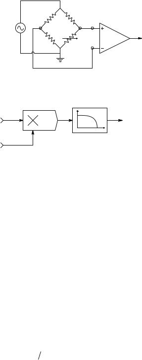
DSBSCM is widely used in instrumentation and measurement systems. For example, it is the natural result when a light beam is chopped in a photonic instrument such as a spectrophotometer; it also results when a Wheatstone bridge is given ac (carrier) excitation and nulled, then one or more arm resistances are slowly varied in time around its null value (see Figure 11.1(A)). DSBSCM is also present at the output of an LVDT (linear variable differential transformer) length sensor as the core is moved in and out (Northrop, 1997). Figure 11.1(B) illustrates a simple system used to demodulate DSBSCM signals.
11.3 Implementation of AM
11.3.1Introduction
Equation 11.1B indicates that multiplication is inherent in the AM process. In practice, an actual analog multiplier can be used or effective multiplication
© 2004 by CRC Press LLC
Modulation and Demodulation of Biomedical Signals |
435 |
R R
Vs |
Vi |
|
Vo |
||
|
||
|
Vi’ DA |
|
R |
R + ∆R |
A
DSBSC |
Analog multiplier |
LPF |
|
|
___ |
||
signal |
|
||
Vm’ |
Vm’ |
||
Vo |
|||
|
|
||
Vref |
B |
|
FIGURE 11.1
(A) A one-active arm Wheatstone bridge. When ac excitation is used, the output is a doublesideband, suppressed-carrier modulated carrier. (B) The use of an analog multiplier and lowpass filter to demodulate a DSBSC signal.
can be realized by passing vc(t) and [1 + m(t)] through a square-law nonlinearity, such as a field-effect transistor. Note that, in Equation 11.1B, m(t) ≤ 1, so [1 + m(t)] ≥ 0. If [1 + m(t)] were to go <0, a 180∞ phase-shift would take place in the AM output, which is an undesirable condition called overmodulation. This condition also occurs when the modulator output stage is driven so hard that the output transistor stage is cut off, giving zero output for several carrier cycles. Hard cut-off also distorts the AM carrier and produces unwanted harmonics in the demodulated signal. Many types of circuits have been devised to do AM. Although all of them cannot be examined here, several are described in the next section.
11.3.2Some Amplitude Modulation Circuits
Figure 11.2 illustrates the use of a JFET as a square-law modulator. The gate–source voltage is the sum of a dc bias voltage, which places the quiescent operating point of the JFET at the center of its saturated channel region, plus the carrier signal and the modulating signal. In this and the following examples, ωm ωc is asserted.
vGS = − |
|
Vp 2 |
|
+ Vc cos(ωct)+ Vm cos(ωmt) |
(11.9) |
|
|
© 2004 by CRC Press LLC
436 |
Analysis and Application of Analog Electronic Circuits |
 +VDD
+VDD
C
RT L
AM out vm(t) 
 iD = IDSS(1 − vGS /VP)2
vc(t) |
vGS |
|
− |
||
|
||
|
VP/2 |
 iD
iD
IDSS
vGS
VP |
0 |
(−4 V)
FIGURE 11.2
Top: schematic of a tuned-output JFET square-law amplitude modulator. Bottom: square-law drain current vs. gate-source voltage curve for a JFET operated under saturated drain conditions [vDS > vGS + VP ].
The JFET’s drain current is then:
|
|
|
− |
|
V |
2 |
|
|
+ V cos ω |
|
t |
+ V cos ω |
t ˆ 2 |
|||||||||||||||||
|
|
|
|
|
||||||||||||||||||||||||||
iD |
= IDSS 1 |
− |
|
|
|
|
|
|
P |
|
|
|
|
c |
|
( |
|
c |
) |
m |
|
( |
|
m ) |
˜ |
|||||
|
|
|
|
|
|
|
|
|
|
|
|
|
VP |
|
|
|
|
|
|
|
||||||||||
|
|
|
|
|
|
|
|
|
|
|
|
|
|
|
|
|
|
|
|
|
|
|
↓ |
|||||||
|
|
|
− |
|
V |
2 |
|
+ V cos ω t |
+ V |
cos ω |
t |
|
ˆ 2 |
|||||||||||||||||
|
|
|
|
|||||||||||||||||||||||||||
|
= IDSS 1 |
+ |
|
|
|
|
|
|
P |
|
|
|
|
c |
|
( |
|
c ) |
m |
|
( |
|
m ) |
|
˜ |
|||||
|
|
|
|
|
|
|
|
|
|
|
|
|
|
|
VP |
|
|
|
|
|
|
|
|
|||||||
|
|
|
|
|
|
|
|
|
|
|
|
|
|
|
|
|
|
|
|
|
|
|
|
|
↓ |
|||||
|
|
|
V |
2 |
|
+ V cos ω t |
+ V |
cos ω |
t ˆ 2 |
|
|
|||||||||||||||||||
|
|
|
|
|
||||||||||||||||||||||||||
|
= IDSS |
|
|
|
P |
|
|
|
|
|
|
|
c |
( |
c |
) |
|
|
|
m |
( |
|
m ) |
˜ |
|
|
|
|||
|
|
|
|
|
|
|
|
|
|
|
|
|
|
|
|
|
VP |
|
|
|
|
|
|
|
|
|
|
|
||
|
|
|
|
|
|
|
|
|
|
|
|
|
|
|
|
|
|
|
|
|
|
|
↓ |
|
|
|
||||
(11.10A)
(11.10B)
(11.10C)
© 2004 by CRC Press LLC
Modulation and Demodulation of Biomedical Signals |
437 |
|
= (IDSS |
VP2 )(VP2 4 + Vc2 cos2 (ωct)+ Vm2 cos2 (ωmt)+ |
(11.10D) |
|
VP[Vc cos(ωct)+ Vm cos(ωmt)]+ 2VcVm[cos(ωct)cos(ωmt)] |
|
iD = (IDSS |
VP2 ){(VP2 4 + Vc2 12[1+ cos2 (2ωct)]+ Vm2 12 [cos2 (2ωmt)]+ |
(11.10E) |
|
VP[Vc cos(ωct)+ Vm cos(ωmt)]+ VcVm[cos((ωct)t)+ cos((ωmta)t)]} |
|
Equation 11.10E shows that the drain current has dc terms, terms at ωm and 2ωm, terms at ωc and 2ωc, and the sideband terms at ωc + ωm and ωc − ωm. The dc terms are eliminated by the output coupling capacitor. The RLC “tank” circuit is resonant around ωc and so selects the ωc and sideband terms. The AM output voltage is approximately:
(11.11) vo −RT (IDSS VP2 ){VPVc cos(ωct)+ VcVm[cos((ωc + ωm )t)+ cos((ωc − ωm )t)]}
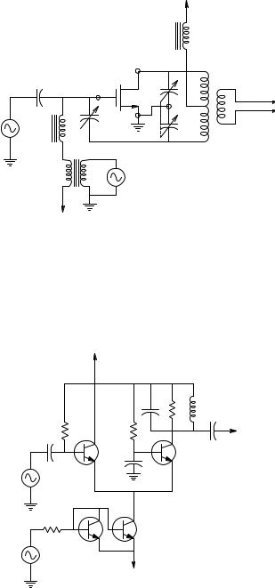
i.e., the resonant circuit attenuates all frequencies not immediately around ωc. Figure 11.3 illustrates the architecture of a class C MOSFET RF power amplifier with a high Q output resonant circuit. The modulating signal, vm(t), is added to a dc gate bias and the RF carrier source. The radio-frequency chokes (RFC) are inductors with very high reactance around ωc; they pass currents from dc to ωmmax. The principle of sideband generation is very similar to the preceding JFET example. JFETs and MOSFETs have square-
law iD vs. vGS curves.
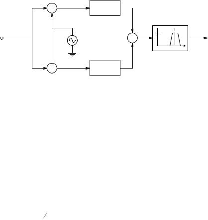
The BJT circuit of Figure 11.4 illustrates another amplitude modulator architecture. Q3 and Q4 modulate the collector currents in Q1 and Q1 by changing the gm of these transistors; for example, gm1 = ICQ1/VT. The operating points of Q1 and Q2 are identical and are affected by IC4 = IE1 + IE2, which is in turn a function of the modulating signal, vm(t). Clarke and Hesse (1971) give a detailed analysis of this transconductance modulator.
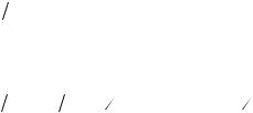
Still another approach to AM generation is illustrated in the block diagram of Figure 11.5. This system is basically a quarter square multiplier, except the nonlinearities contain a linear (a1) term as well as the square-law (a2) term. The signals are:
w(t) = Vc cos(ωct)+ [1+ m(t)], |
|
mmax |
|
≤ 1. |
(11.12A) |
|
|
||||
z(t) = Vc cos(ωct)− [1+ m(t)], |
(11.12B) |
||||
© 2004 by CRC Press LLC
438 |
|
Analysis and Application of Analog Electronic Circuits |
|
|
|
|
+VDD |
|
|
|
RFC |
|
|
|
D |
|
|
G |
CT |
|
|
|
|
|
|
|
AM out |
|
|
|
S |
vc(t) |
RFC |
CN |
|
|
|
|
Tank |
|
Modulation |
|
|
|
xfmr |
|
vm(t) |
VGG
FIGURE 11.3
A class C MOSFET tuned RF power amplifier in which the low-frequency modulating signal is added to the carrier voltage at the gate. Miller input capacitance at the gate is cancelled by positive feedback through the small neutralizing capacitor, CN.
+VCC
C
RT L
AM out
RB1 |
RB1 |
Q1 |
Q2 |
vc(t)
RB3
Q3 Q4
vm(t)
−VEE
FIGURE 11.4
A transconductance-type amplitude modulator using npn BJTs. The circuit effectively multiplies the carrier by the modulating signal, producing an AM output.
© 2004 by CRC Press LLC
Modulation and Demodulation of Biomedical Signals |
439 |
||
+ |
w |
a1w + a2w2 |
|
|
|
||
|
+ |
|
|
|
|
BPF |
|
[1 + m(t)] |
+ |
1 |
|
|
x |
y |
|
vc(t) |
− |
|
AM |
|
|
||
|
ωc |
out |
 +
+
− |
z |
a1z + a2z2 |
|
FIGURE 11.5
Block diagram of a quarter-square multiplier used for amplitude modulation.
u(t) = a1Vc cos(ωct) + a1[1 + m(t)]+
(11.12C)
a2 {Vc2 cos2 (ωct) + 2Vc [1 + m(t)]cos(ωct) + [1 + 2m(t) + m2 (t)]}
v(t) = a1Vc cos(ωct)− a1[1+ m(t)]+ |
(11.12D) |
a2 {Vc2 cos2 (ωct)− 2Vc[1+ m(t)]cos(ωct)+ [1+ 2m(t) + m2 (t)]} |
|
x = u − v |
(11.12E) |
x(t) = 2a1 + 2a1mc cos(ωmt) + (4a2Vc )cos(ωct) +
(11.12F)
(4a2Vc ) 12 {cos[(ωc + ωm )t]+ cos[(ωc − ωm )t]}
The band-pass filter around (ωc − ωm) to (ωc + ωm) selects the AM output and blocks dc and ωm. Many other AM circuits exist; some are practical for high-power RF output while others assume the AM output will be amplified by a linear RF amplifier.
Double-sideband suppressed carrier modulation (DSBSCM) is another form of AM in which little or no carrier frequency power occurs in the output spectrum. Ideally, DSBSCM follows Equation 11.1C, i.e., DSBSCM results as the product of a low-frequency modulating signal multiplying a high-fre- quency carrier voltage.
Many processes are inherent generators of DSBSCM. For example, see Figure 11.1(A) for a Wheatstone bridge initially nulled, whose output depends on R/R. The bridge is given ac excitation so that its sensitivity will be enhanced. Developing an expression for Vo using voltage-divider relations,
V = V |
R + |
R |
(11.13) |
|
R |
||
i s 2R + |
|
||
© 2004 by CRC Press LLC

440 |
Analysis and Application of Analog Electronic Circuits |
|||
|
V′= V |
R |
(11.14) |
|
|
|
|||
|
i |
s 2R |
|
|
The output is found by subtracting Vi′ from Vi and multiplying the difference by the DA’s gain, KD.
V = K V |
|
R |
|
˘ |
K V |
R 4R |
] |
= (K V |
4R) |
R(t)cos(ω |
t) |
(11.15) |
|
|
|||||||||||
o D s |
4R + 2 |
|
˙ |
D s[ |
|
D s |
[ |
c |
] |
|||
|
|
R ˚ |
|
|
|
|
|
|
|
|
||
The quantity in the brackets is the DSBSCM product. R(t) varies at ωm. DSBSCM occurs for light-beam chopping in photonic systems, as well as
for the output of the linear variable differential transformer (LVDT) linear position sensor. A schematic of an LVDT is shown in Figure 11.6. Seen on end, an LVDT is a cylinder with a tube in the center running the length of the cylinder. In the center of the tube slides a cylindrical, high-permeability magnetic core that couples magnetic flux from the excitation core to the two secondary coils, which are wound in opposite directions with the same number of turns. When the core is centered (x = 0), equal flux intercepts the winding of both secondary coils and the output EMF is zero. If the core position is up (x = +xm), most of the flux is coupled to the upper secondary coil and Vo is maximum, having the same phase as Vc. If x = −xm, Vo is maximum and the phase is 180∞ from Vo with x = +xm. In general, the linear part of the output can be written as:
|
∞ |
∞ ˆ |
= K x(t)Vc cos(ωct) |
|
Vo = N |
ϕu |
− ϕ1↓ |
(11.16) |
where ϕ°u is the time rate of change of the ac flux intercepting the N turns of the upper secondary coil and K is the slope of the linear Vo vs. x curve.
Refer to Figure 11.5. If [1 + m(t)] is replaced by vm(t), it is easy to see that the output x(t) is given by:
x(t) = u(t) − v(t) = 2a1vm (t) + 4a2vc (t)vm (t) |
(11.17) |
= 2a1Vm cos(ωmt)+ 2a2VcVm[cos((ωc + ωm )t)+ cos((ωc − ωm )t)]
The BPF centered on ωc removes the 2a1Vm cos(ωmt) term, leaving the DSBSCM output; thus,
y(t) = 2a2VcVm[cos((ωc + ωm )t)+ cos((ωc − ωm )t)] |
(11.18) |
DSBSCM is widely encountered in all phases of instrumentation and measurement systems; it is the direct result of multiplying the carrier times the modulating signal.
© 2004 by CRC Press LLC