

- •Analysis and Application of Analog Electronic Circuits to Biomedical Instrumentation
- •Dedication
- •Preface
- •Reader Background
- •Rationale
- •Description of the Chapters
- •Features
- •The Author
- •Table of Contents
- •1.1 Introduction
- •1.2 Sources of Endogenous Bioelectric Signals
- •1.3 Nerve Action Potentials
- •1.4 Muscle Action Potentials
- •1.4.1 Introduction
- •1.4.2 The Origin of EMGs
- •1.5 The Electrocardiogram
- •1.5.1 Introduction
- •1.6 Other Biopotentials
- •1.6.1 Introduction
- •1.6.2 EEGs
- •1.6.3 Other Body Surface Potentials
- •1.7 Discussion
- •1.8 Electrical Properties of Bioelectrodes
- •1.9 Exogenous Bioelectric Signals
- •1.10 Chapter Summary
- •2.1 Introduction
- •2.2.1 Introduction
- •2.2.4 Schottky Diodes
- •2.3.1 Introduction
- •2.4.1 Introduction
- •2.5.1 Introduction
- •2.5.5 Broadbanding Strategies
- •2.6 Photons, Photodiodes, Photoconductors, LEDs, and Laser Diodes
- •2.6.1 Introduction
- •2.6.2 PIN Photodiodes
- •2.6.3 Avalanche Photodiodes
- •2.6.4 Signal Conditioning Circuits for Photodiodes
- •2.6.5 Photoconductors
- •2.6.6 LEDs
- •2.6.7 Laser Diodes
- •2.7 Chapter Summary
- •Home Problems
- •3.1 Introduction
- •3.2 DA Circuit Architecture
- •3.4 CM and DM Gain of Simple DA Stages at High Frequencies
- •3.4.1 Introduction
- •3.5 Input Resistance of Simple Transistor DAs
- •3.7 How Op Amps Can Be Used To Make DAs for Medical Applications
- •3.7.1 Introduction
- •3.8 Chapter Summary
- •Home Problems
- •4.1 Introduction
- •4.3 Some Effects of Negative Voltage Feedback
- •4.3.1 Reduction of Output Resistance
- •4.3.2 Reduction of Total Harmonic Distortion
- •4.3.4 Decrease in Gain Sensitivity
- •4.4 Effects of Negative Current Feedback
- •4.5 Positive Voltage Feedback
- •4.5.1 Introduction
- •4.6 Chapter Summary
- •Home Problems
- •5.1 Introduction
- •5.2.1 Introduction
- •5.2.2 Bode Plots
- •5.5.1 Introduction
- •5.5.3 The Wien Bridge Oscillator
- •5.6 Chapter Summary
- •Home Problems
- •6.1 Ideal Op Amps
- •6.1.1 Introduction
- •6.1.2 Properties of Ideal OP Amps
- •6.1.3 Some Examples of OP Amp Circuits Analyzed Using IOAs
- •6.2 Practical Op Amps
- •6.2.1 Introduction
- •6.2.2 Functional Categories of Real Op Amps
- •6.3.1 The GBWP of an Inverting Summer
- •6.4.3 Limitations of CFOAs
- •6.5 Voltage Comparators
- •6.5.1 Introduction
- •6.5.2. Applications of Voltage Comparators
- •6.5.3 Discussion
- •6.6 Some Applications of Op Amps in Biomedicine
- •6.6.1 Introduction
- •6.6.2 Analog Integrators and Differentiators
- •6.7 Chapter Summary
- •Home Problems
- •7.1 Introduction
- •7.2 Types of Analog Active Filters
- •7.2.1 Introduction
- •7.2.3 Biquad Active Filters
- •7.2.4 Generalized Impedance Converter AFs
- •7.3 Electronically Tunable AFs
- •7.3.1 Introduction
- •7.3.3 Use of Digitally Controlled Potentiometers To Tune a Sallen and Key LPF
- •7.5 Chapter Summary
- •7.5.1 Active Filters
- •7.5.2 Choice of AF Components
- •Home Problems
- •8.1 Introduction
- •8.2 Instrumentation Amps
- •8.3 Medical Isolation Amps
- •8.3.1 Introduction
- •8.3.3 A Prototype Magnetic IsoA
- •8.4.1 Introduction
- •8.6 Chapter Summary
- •9.1 Introduction
- •9.2 Descriptors of Random Noise in Biomedical Measurement Systems
- •9.2.1 Introduction
- •9.2.2 The Probability Density Function
- •9.2.3 The Power Density Spectrum
- •9.2.4 Sources of Random Noise in Signal Conditioning Systems
- •9.2.4.1 Noise from Resistors
- •9.2.4.3 Noise in JFETs
- •9.2.4.4 Noise in BJTs
- •9.3 Propagation of Noise through LTI Filters
- •9.4.2 Spot Noise Factor and Figure
- •9.5.1 Introduction
- •9.6.1 Introduction
- •9.7 Effect of Feedback on Noise
- •9.7.1 Introduction
- •9.8.1 Introduction
- •9.8.2 Calculation of the Minimum Resolvable AC Input Voltage to a Noisy Op Amp
- •9.8.5.1 Introduction
- •9.8.5.2 Bridge Sensitivity Calculations
- •9.8.7.1 Introduction
- •9.8.7.2 Analysis of SNR Improvement by Averaging
- •9.8.7.3 Discussion
- •9.10.1 Introduction
- •9.11 Chapter Summary
- •Home Problems
- •10.1 Introduction
- •10.2 Aliasing and the Sampling Theorem
- •10.2.1 Introduction
- •10.2.2 The Sampling Theorem
- •10.3 Digital-to-Analog Converters (DACs)
- •10.3.1 Introduction
- •10.3.2 DAC Designs
- •10.3.3 Static and Dynamic Characteristics of DACs
- •10.4 Hold Circuits
- •10.5 Analog-to-Digital Converters (ADCs)
- •10.5.1 Introduction
- •10.5.2 The Tracking (Servo) ADC
- •10.5.3 The Successive Approximation ADC
- •10.5.4 Integrating Converters
- •10.5.5 Flash Converters
- •10.6 Quantization Noise
- •10.7 Chapter Summary
- •Home Problems
- •11.1 Introduction
- •11.2 Modulation of a Sinusoidal Carrier Viewed in the Frequency Domain
- •11.3 Implementation of AM
- •11.3.1 Introduction
- •11.3.2 Some Amplitude Modulation Circuits
- •11.4 Generation of Phase and Frequency Modulation
- •11.4.1 Introduction
- •11.4.3 Integral Pulse Frequency Modulation as a Means of Frequency Modulation
- •11.5 Demodulation of Modulated Sinusoidal Carriers
- •11.5.1 Introduction
- •11.5.2 Detection of AM
- •11.5.3 Detection of FM Signals
- •11.5.4 Demodulation of DSBSCM Signals
- •11.6 Modulation and Demodulation of Digital Carriers
- •11.6.1 Introduction
- •11.6.2 Delta Modulation
- •11.7 Chapter Summary
- •Home Problems
- •12.1 Introduction
- •12.2.1 Introduction
- •12.2.2 The Analog Multiplier/LPF PSR
- •12.2.3 The Switched Op Amp PSR
- •12.2.4 The Chopper PSR
- •12.2.5 The Balanced Diode Bridge PSR
- •12.3 Phase Detectors
- •12.3.1 Introduction
- •12.3.2 The Analog Multiplier Phase Detector
- •12.3.3 Digital Phase Detectors
- •12.4 Voltage and Current-Controlled Oscillators
- •12.4.1 Introduction
- •12.4.2 An Analog VCO
- •12.4.3 Switched Integrating Capacitor VCOs
- •12.4.6 Summary
- •12.5 Phase-Locked Loops
- •12.5.1 Introduction
- •12.5.2 PLL Components
- •12.5.3 PLL Applications in Biomedicine
- •12.5.4 Discussion
- •12.6 True RMS Converters
- •12.6.1 Introduction
- •12.6.2 True RMS Circuits
- •12.7 IC Thermometers
- •12.7.1 Introduction
- •12.7.2 IC Temperature Transducers
- •12.8 Instrumentation Systems
- •12.8.1 Introduction
- •12.8.5 Respiratory Acoustic Impedance Measurement System
- •12.9 Chapter Summary
- •References

Digital Interfaces |
397 |
10.3 Digital-to-Analog Converters (DACs)
10.3.1Introduction
A digital-to-analog converter accepts as inputs an N-bit digital word (0s and 1s) representing a numerical value of an analog output signal and a convert enable (CE) command. A DAC’s output is a voltage or current determined by the digital word input. The output is held until the next word is presented (as parallel or serial data) and the next CE command is given. DACs (voltage or current output) are used in many applications that include but are not limited to: high-fidelity sound systems; analog CRT display systems used in computers and TV; generation of analog signals used in test and measurement systems, etc.
10.3.2DAC Designs
DACs can be classified by whether they use bipolar junction transistor switches or MOS transistor technology. The following DAC architectures are found with MOS technology:
•Binary-weighted resistor DAC
•R–2R ladder
•Inverted R–2R ladder
•Inherent monolithic ladder
•Switched-capacitor DAC
The following DAC designs use BJT technology:
•Binary-weighted current sources
•R–2R ladder using current sources
Figure 10.4 illustrates four common DAC architectures. Figure 10.4(A) shows the binary weighted resistor DAC. This is an impractical design for IC fabrication; one needs accurate resistor ratios over a wide range of resistor values. Also, the op amp is presented with varying input impedances, depending on the input word, thus making the DAC subject to op amp DC bias current errors. The SPDT switches used in this design are generally MOS transistors designed to have very low ON resistance and high OFF resistance. The output voltage of this DAC is given by:
|
−VR |
N |
|
|
Vo = |
bk 2 |
k |
(10.11) |
|
2N |
|
|||
|
|
k =1 |
|
|
© 2004 by CRC Press LLC
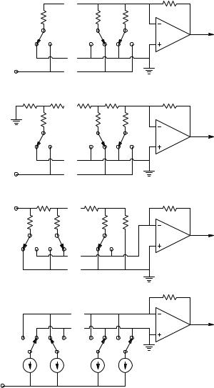
398 |
Analysis and Application of Analog Electronic Circuits |
A
B
C
D
−VR
|
|
|
|
|
R |
|
|
. . . |
|
|
|
2NR |
|
4R |
2R |
|
|
|
bN |
|
b2 |
|
Vo |
|
|
|
b1 |
||
0 |
1 |
1 |
0 |
0 |
1 |
|
|
. . . |
|
|
|
VR |
|
. . . |
|
|
|
|
|
|
|
|
|
2R |
R |
R |
R |
R |
|
|
|
. . . |
|
|
|
|
2R |
|
2R |
2R |
|
|
bN |
|
b2 |
|
Vo |
|
|
|
b1 |
||
0 |
1 |
0 |
1 |
0 |
1 |
|
|
. . . |
|
|
|
VR |
|
. . . |
|
|
|
|
|
|
|
|
|
VR |
R |
. . . |
R |
|
R |
|
|
|
|
|
|
2R |
2R |
|
2R |
2R |
|
b1 |
|
b2 |
|
bN |
Vo |
|
|
|
|||
0 |
1 0 |
1 |
0 |
1 |
|
|
|
. . . |
|
|
|
|
|
. . . |
|
|
|
|
|
|
|
|
R |
|
|
. . . |
|
|
Vo |
|
|
|
|
|
|
|
|
. . . |
|
|
|
1 |
0 1 |
10 . . . 1 |
0 |
0 |
|
bN |
|
bN−1 |
b2 |
|
b1 |
Io /2N |
Io /2N−1 |
|
Io /4 |
Io /2 |
|
FIGURE 10.4
Four kinds of DAC circuits using op amps: (A) a binary-weighted resistor DAC (not practical for N > 8); (B) the R–2R ladder DAC; (C) the inverted R–2R ladder DAC; and (D) a binaryweighted current source DAC (not practical for N > 8).
where N is the bit length of the binary “word” being converted and bk is “0” or “1,” depending on the word.
Figure 10.4(B) illustrates the popular R–2R ladder DAC. Here only two resistor values are used; their exact values are not critical, but the ratio must
© 2004 by CRC Press LLC
Digital Interfaces |
399 |
be exactly 2 between all 2R and R valued resistors. Switches with low ON resistance and zero offset voltage are required. The output can be shown to be:
|
−V |
−VR |
k |
|
|
Vo = |
|
R |
bk 2 |
(10.12) |
|
2 |
N+1 |
|
|||
|
|
2N +1 |
|
|
|
|
|
|
|
|
|
Full-scale output voltage occurs when all the switches are set to VR. This is:
V |
= −V |
2N − 1 |
|
(10.13) |
|
||||
oFS |
R 2N |
|
||
The inverted R–2R DAC architecture is shown in Figure 10.4(C). This is a relatively switching glitch-free DAC, well suited for CMOS switches. Note that the ladder resistors’ currents are constant and independent of the switch positions because the op amp’s summing junction is at virtual ground. Bit b1 is the most significant bit (MSB). With b1 = 1 and all others = 0, Vo = −VR/2.
Figure 10.4(D) illustrates the overall architecture of the binary-weighted current source DAC. This circuit is easily implemented with BJT current sources and switches. There are a number of approaches to realizing the switches and current sources for this type of DAC (Franco, 1988). The output voltage of this DAC is given by:
N |
|
Vo = (IoR) bk 2−k |
(10.14) |
k =1
When the MSB is HI (b1 = 1) and all other bk = 0, Vo = Io R/2; when the LSB is HI (bN = 1) and all other bk = 0, then Vo = Io R/2N.
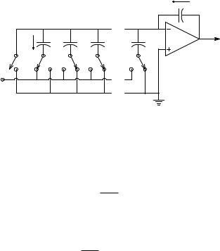
Figure 10.5 illustrates a simplified schematic of a low-power DAC using switched weighted capacitors (SWC). The MSB output of the SWC DAC can be found by observing that when b1 1, all other bk = 0, and the charge in C1 is also the charge in CF. Also, the summing junction is assumed to be at virtual ground. Thus:
Q |
1 |
= 2N−1 C V |
R |
= Q |
F |
= V 2N C |
(10.15) |
|
|
|
o |
|
|||
|
|
|
¬ |
|
|
|
|
|
|
Vo = VR/2 |
|
(10.16) |
|||
The LSB output of the SWC DAC is found the same way: by assuming bN 1, all other bk = 0.
© 2004 by CRC Press LLC
400 |
|
Analysis and Application of Analog Electronic Circuits |
|||||
|
|
|
|
|
|
|
QF |
|
|
|
|
|
|
|
C 2N |
|
|
|
|
. . . |
|
(0) |
CF |
|
|
|
|
|
Vo |
||
|
CN |
C |
2C |
4C |
C1 |
C 2N −1 |
|
|
|
||||||
Reset |
bN |
(LSB) |
|
bN−2 |
b1 |
(MSB) |
|
|
1 |
0 1 |
0 1 |
0 |
1 0 |
|
|
VR < 0 |
|
|
|
. . . |
|
|
|
|
|
|
|
|
|
|
|
|
|
|
|
. . . |
|
|
|
FIGURE 10.5 |
|
|
|
|
|
|
|
A switched, weighted capacitor DAC (not practical for N > 8). |
|
||||||
QN = VR 20 C = QF = Vo 2N C
¬
V = VR
o 2N−1
The general output can be written:
N
V = VRC b 2k−1
o 2N k k =1
(10.17)
(10.18)
(10.19)
Some practical problems emerge in considering the SWC DAC: (1) C1 must have 2N−1 times the area of CN on the substrate. This limits N practically to 8.
(2) The op amp must have a MOS transistor front end to obtain ultra-low bias current so that Vo will not significantly drift over a sampling period.
In Figure 10.6, a design strategy enables the use of a 1:8 capacitor area ratio, rather than a 1:128 area ratio required for the 8-bit DAC shown in Figure 10.5. The MSB output is found from the capacitive voltage divider made from the input array. The input capacitor is C1 = C. It can be shown that the seriesparallel combination of the rest of the capacitors having bk = 0, so they are grounded is C. Thus, Vo(MSB) is simply VR/2. The LSB output is found the same way by considering the capacitor voltage divider; it can be shown to be Vo(LSB) = VR/256. The complete charge-scaling DAC output is given by:
N |
|
Vo = Vr bk 2−k |
(10.20) |
k =1
Multiplying DACs (MDACs) are a special class of DAC in which the reference signal is made variable and the DAC output is the product of the analog value of vR(t) and the digital scaling input. Thus two-quadrant multiplication can be realized for a straight unipolar binary input:
© 2004 by CRC Press LLC
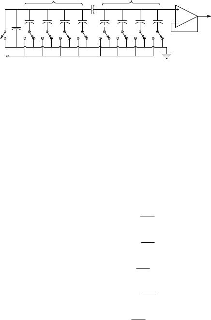
Digital Interfaces |
|
|
|
|
|
|
|
|
|
|
|
|
|
401 |
||
|
|
|
|
LSB array |
|
|
|
|
|
MSB array |
|
|
|
|||
|
|
|
|
|
|
|
|
2C/15 |
|
|
|
|
|
|
|
|
|
|
|
|
|
|
|
|
|
|
|
|
|
|
|
|
Vo |
|
C/8 |
|
C/4 |
|
C/2 |
C |
C |
|
/8 |
|
C/4 |
|
C/2 |
|
|
|
|
C/8 |
|
|
|
|
|
|
|
|
|
|
|
|
|
|
|
Reset |
b8 |
(LSB) |
b7 |
|
b6 |
|
b5 |
|
b4 |
|
b3 |
|
b2 |
|
b1 |
(MSB) |
|
1 |
0 |
1 |
0 |
1 |
0 |
1 |
0 |
1 |
0 |
1 |
0 |
1 |
0 |
1 |
0 |
VR |
|
|
|
|
|
|
|
|
|
|
|
|
|
|
|
|
FIGURE 10.6 |
|
|
|
|
|
|
|
|
|
|
|
|
|
|
|
|
A charge-scaling switched-capacitor DAC. |
|
|
|
|
|
|
|
|
||||||||
|
|
|
|
|
|
|
|
|
|
|
N |
˘ |
|
|
|
|
|
|
|
|
|
|
|
|
|
|
|
|
˙ |
|
|
|
|
|
|
|
|
|
|
vo (t) = vR (t) 2−N |
|
2k ˙ |
|
|
|
(10.21) |
||||
|
|
|
|
|
|
|
|
|
|
|
k =1 |
˚ |
|
|
|
|
If the DAC is set up for bipolar offset binary (BOB) operation, true fourquadrant multiplication occurs. The output of a DAC configured for BOB, such as the AD7845 12-bit MDAC, is given by:
|
|
|
1 |
N |
˘ |
vo (t) = vR |
(t) −1+ |
|
bk |
2k−1˙ |
|
2 |
N−1 |
||||
|
|
|
k =1 |
˙ |
|
|
|
|
|
˚ |
For N = 12:
{bk} = 1111 1111 1111, Vo = vR (t) 20472048
{bk} = 1000 0000 0001, Vo = vR (t) 20481
{bk} = 1000 0000 0001, Vo = vR (t) 20480 = 0
{bk} = 0111 1111 1111, Vo = −vR (t) 20481
{bk} = 0000 0000 0000, Vo = −vR (t) 20482048 = −vR (t)
(10.22)
(10.23A)
(10.23B)
(10.23C)
(10.23D)
(10.23E)
MDACs find application in waveform generation; digitally controlled attenuators; programmable power supplies; programmable gain amplifiers;
© 2004 by CRC Press LLC