

General Properties of Electronic Single-Loop Feedback Systems |
175 |
clear that four major types of feedback exist: (1) negative voltage feedback;
(2) negative current feedback; (3) positive voltage feedback; and (4) positive current feedback. Negative voltage feedback is most widely encountered in electronic engineering practice. Its properties will be examined in the following sections.
4.3Some Effects of Negative Voltage Feedback
4.3.1Reduction of Output Resistance
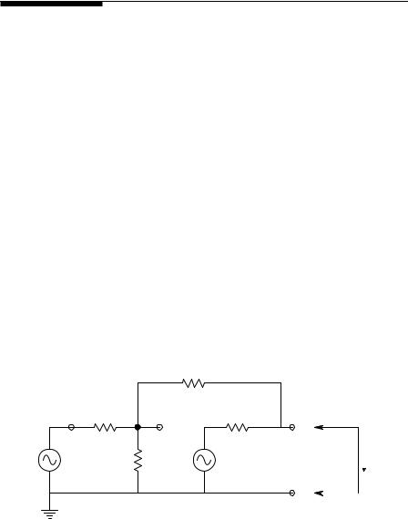
Figure 4.2 illustrates a simple Thevenin amplifier circuit with NVB applied to its summing junction (input node). Assume that the amplifier’s input resistor, Rin, RF and Rs, so Rin can be ignored in writing the node equation for Vi. Also, in finding the NFB amplifier’s open-circuit voltage gain, assume that Ro RF, so negligible voltage drop takes place across Ro. Thus, the node equation is:
|
Vi [Gs + GF] − Vo GF = Vs Gs |
|
(4.3) |
|||
Also, |
|
|
|
|
|
|
|
|
Vo −KvVi |
|
(4.4) |
||
Thus: |
|
|
|
|
|
|
|
|
Vi = −Vo/Kv |
|
(4.5) |
||
and |
|
|
|
|
|
|
|
−(Vo/Kv)(Gs + GF) − Vo GF = Vs Gs |
(4.6) |
||||
|
|
RF |
|
|
|
|
Rs |
Vi |
Ro |
Vo |
SC |
||
|
|
|
|
|||
+ |
|
− |
|
|
|
IoSC |
|
|
|
|
|||
Vs |
Ri |
KvVi |
|
|
|
|
|
|
+ |
|
|
|
|
|
|
|
|
|
|
|
|
|
|
|
|
|
|
FIGURE 4.2
Schematic of a simple Thevenin VCVS with negative feedback. See text for analysis.
© 2004 by CRC Press LLC

176 Analysis and Application of Analog Electronic Circuits
Thus, Equation 4.6 can be used to write the closed-loop system’s transfer
function: |
|
|
|
|
|
|
||
|
Vo |
= |
−Kv Gs |
= |
−KvRF (RF + Rs ) |
= A |
(4.7) |
|
|
|
|
|
|||||
|
Vs |
Gs + GF + KvGF |
|
1+ KvRs (RF + Rs ) |
v |
|
||
|
|
|
|
|||||
Note in comparing Equation 4.7 to Equation 4.1, that |
|
|
||||||
AL = −Kv [Rs/(RF + Rs)] (Note: system has NFB.) |
(4.8) |
|||||||
α = RF/(RF + Rs) |
|
|
|
|
(4.9) |
|||
β = Rs/(RF + Rs) |
|
|
|
|
(4.10) |
|||
In op amps, Kv is numerically very large, so Equation 4.7 reduces to the well-known gain relation for the ideal op amp inverter: Vo/Vs = −RF/Rs.)
There are two common ways to find the output resistance of the simple NFB amplifier of Figure 4.2. One is to set Vs = 0, then place an independent test source, Vt, between the Vo node and ground and calculate Rout = Vt/It. The other method is to measure the open-circuit output voltage using Equation 4.7, then calculate the short-circuit output current (with Vo = 0). Clearly, Rout = VOC/IoSC. Inspection of Figure 4.2 with a shorted output lets one write:
|
= |
|
V |
|
− |
K R ˘ |
|
−V K R |
|
|
IoSC |
|
s |
1 |
v F |
˙ |
s v F |
(4.11) |
|||
(Rs |
|
|
Ro (RF + Rs ) |
|||||||
|
|
+ RF ) |
|
Ro ˚ |
|
|
||||
Now Rout can be found: |
|
|
|
|
|
|
||||||
|
|
−KvRF |
(RF + Rs ) |
|
|
|
|
|
|
|||
R = |
|
1+ KvRs |
(RF + Rs ) |
= |
Ro |
= |
Ro |
= |
Ro |
(4.12) |
||
|
|
−VsKvRF |
|
1+ KvRs (RF + Rs ) |
1+ βKv |
1− AL |
||||||
out |
|
|
|
|
|
|
||||||
|
|
|
|
|
|
|
|
|||||
|
|
|
Ro (RF + Rs ) |
|
||||||||
|
|
|
|
|
|
|
|
|
||||
In general, the NFB amplifier’s output impedance can be written as a function of frequency:
Zout(jω) = Ro/RD(jω) |
(4.13) |
Note that, in general, Zout(jω) is very small (e.g., milliohms) at dc and low frequencies, then gradually increases with ω. This property can be demonstrated by assuming Kv to have a frequency response of the form:
Kv(jω) = |
Kvo |
|
(4.14) |
|
jωτ + 1 |
||||
|
|
|||
© 2004 by CRC Press LLC

General Properties of Electronic Single-Loop Feedback Systems |
|
|
|
|
177 |
||||||||||||
Equation now yields: |
|
|
|
|
|
|
|
|
|
|
|
|
|
|
|||
|
|
Ro |
|
|
Ro (jωτ + 1) |
|
[ o |
( |
+ βK |
vo )]( |
|
) |
|
||||
Zo(jω) = |
|
|
|
= |
|
|
|
|
= |
R |
1 |
|
|
jωτ + 1 |
(4.15) |
||
1+ βK |
vo ( |
) |
jωτ + |
( |
+ βK |
vo ) |
|
jωτ |
( |
βK |
vo ) |
+ 1 |
|||||
|
|
jωτ + 1 |
|
1 |
|
|
|
1+ |
|
|
|
||||||
From the preceding equation it is clear that Zo Ro/βKvo at dc, increasing with frequency to Zo = Ro at frequencies above βKvo/τ r/s.
4.3.2Reduction of Total Harmonic Distortion
A very important property of NFB is the reduction of total harmonic distortion (THD) at the output of amplifiers, in particular power amplifiers. First it is necessary to examine what THD means. Assume that a certain amplifier has a soft saturation nonlinearity modeled by:
y = ax + bx2 + cx3 + dx4 + ex5 +… |
(4.16) |
Clearly, a = Kv, the linear gain. The b, c, d, e, … terms can be zero or have either sign. They give rise to the harmonic distortion that can be the result of transistor cut-off or saturation, or power supply saturation. If x(t) = Xo sin(ωot), the output y(t) will contain the desired fundamental frequency from the a-term, as well as unwanted harmonics. For example,
y(t) = a Xo sin(ωot) + (bXo2  2)[1 − cos(2ωot)]+ (cXo3
  4)
4)
(4.17)
[3 sin(ωot) − sin(3ωot)]+ ≡
The power terms approximating the nonlinear transfer characteristic of the amplifier generate dc, fundamental, and harmonics of the order of the nonlinear term in addition to the desired fundamental frequency. These can be summarized by the expression:
y(t) = Kv Xo sin(ωot) + H2 sin(2ωot) + H3 sin(3ωot) + H4 sin(4ωot) +… (4.18)
The total RMS harmonic distortion is defined as:
• |
|
THD = H22 2 + H32 2 + H42 2 + ≡ = Hk2 2 |
(4.19) |
k=2
Note that Hk2/2 is the mean squared value of the kth harmonic; (Kv2Xo2/2) is the MS value of the fundamental frequency (desired) component of the output. In general, the larger Xo is, the larger will be the THD.
© 2004 by CRC Press LLC

178 |
|
Analysis and Application of Analog Electronic Circuits |
||||||
NFB System with Output Distortion |
|
vd (vos) |
|
|||||
|
|
|
||||||
|
|
|
|
|
|
+ |
|
|
|
α |
|
|
|
+ |
|
Vo |
|
Vs |
|
− |
Kv |
|
|
|
||
|
|
|
|
|
|
|
||
|
|
|
|
β |
|
|
|
|
|
|
|
|
A |
|
|
|
|
rms |
vos1 |
|
|
|
|
|
|
|
|
|
|
|
|
|
|
||
|
|
|
Output Harmonics |
|
|
|||
|
|
|
vd |
|
|
|
|
|
|
|
vd2 |
|
|
vd |
|
|
|
|
|
|
|
|
|
vd |
||
|
|
|
|
vd |
|
|
||
|
|
|
|
|
vd |
|
||
0 |
|
|
|
|
|
ω (r/s) |
||
|
|
|
|
|
|
|||
ωo |
2ωo |
3ωo |
4ωo |
5ωo |
6ωo |
7ωo |
||
0 |
||||||||
B
THD (rmsV)
Harmonic Generation
THD1
vos
0 |
|
|
|
0 |
vos |
VCL |
C
FIGURE 4.3
(A)Block diagram of a SISO negative voltage feedback system with output harmonic distortion voltage introduced in the last (power) stage. A sinusoidal input of frequency ωo is assumed.
(B)Rms power spectrum of the feedback amplifier output. vos1 is the RMS amplitude of the fundamental frequency output. (C) Plot of how total harmonic distortion typically varies as a function of the amplitude of the fundamental output voltage.
Figure 4.3(A) illustrates a block diagram showing how the RMS THD is added to the output of an NFB amplifier. Distortion is assumed to occur in the last stage. If there were no feedback, (β = 0), Vo = Vs αKv + vd (VsαKv). Vs is adjusted so that the RMS output signal is vos1. With feedback,
© 2004 by CRC Press LLC

General Properties of Electronic Single-Loop Feedback Systems |
179 |
|||||
|
vos1 |
|
THD |
|
||
|
|
vd (vos1) |
|
|
||
V = |
VsαKv |
+ |
|
(4.20) |
||
1+ β Kv |
1+ β Kv |
|||||
o |
|
|
||||
|
|
|
|
|
||
With NFB, the output THD is reduced by a factor of 1/(1 + β Kv), given that the signal output is the same in the nonfeedback and the feedback cases. This result has vast implications in the design of nearly distortion-free audio power amplifiers, as well as linear signal conditioning systems in general that use op amps. vdk in Figure 4.3(B) is simply the kth RMS harmonic voltage; i.e., vdk = Hk/ 2. Figure 4.3(C) shows how the RMS THD increases as the signal output is made larger. At vos = VCL, the level of distortion increases abruptly because the amplifier begins to saturate and clip the output signal waveform.
In good low-distortion amplifier design, the input stages are made as linear as possible, and the amplifier is designed so that the output (power) stage saturates before the input and intermediate gain stages do. This allows the THD voltage to effectively be added in the last stage, and thus the THD is reduced by a factor of 1/(1 − AL) = 1/RD.
4.3.3Increase of NFB Amplifier Bandwidth at the Cost of Gain
It is axiomatic in the design of electronic circuit that negative feedback allows one to extend closed-loop amplifier bandwidth (BW) at the expense of dc or mid-band gain. Another way of looking at the effect of NFB on BW is to observe that every amplifier is endowed with some gain*bandwidth product (GBWP); as a figure of merit, larger is better. GBWP remains relatively constant as feedback is applied, so when NFB reduces gain, it increases BW. The frequency-compensated (FC) op amp makes an excellent example of GBWP constancy. The open-loop gain of an FC op amp can be given by:
|
Vo |
|
|
= |
Kvo |
|
(4.21) |
||
V |
− V |
′ |
sτ |
a |
+ 1 |
|
|||
i |
i |
|
|
|
|
|
|
|
|
Note that the op amp is a difference amplifier and has a gain*bandwidth product:
GBWPoa = Kvo/(2πτa) Hertz |
(4.22) |
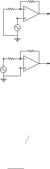
Now connect the OA as a simple noninverting amplifier, as shown in Figure 4.4(A). The amplifier’s output is:
Vo = (Vs − βVo)Kvo/(sτa + 1) |
(4.23) |
© 2004 by CRC Press LLC
180 |
Analysis and Application of Analog Electronic Circuits |
RF
R1 Vi’
Vo
OA
Vi
+
Vs
A
|
|
RF |
|
R1 |
Vi’ |
|
|
|
|
|
Vo |
+ |
|
OA |
Vs |
|
Vi |
|
|
B
FIGURE 4.4
(A) An op amp connected as a noninverting amplifier. (B) An op amp connected as an inverting amplifier.
where
β ∫ R1/(R1 + RF)
Solving for the voltage gain yields:
Vo |
= A (s) = |
Kvo |
(1+ βKvo ) |
|
Vs |
sτa (1+ βKvo )+ 1 |
|||
v |
||||
|
|
|
||
The GBWP for this closed-loop amplifier is simply:
GBWPamp = |
Kvo |
(1+ βKvo ) |
= GBWPoa |
(1+ βKvo ) |
|
||
2πτa |
(4.24)
(4.25)
(4.26)
For the closed-loop feedback amplifier to have exactly the same GBWP as the open-loop op amp is a special case. Note that the closed-loop gain is divided by the RD and the closed-loop BW is multiplied by the RD.
Next, consider the gain, BW, and GBWP of a simple op amp inverter, shown in Figure 4.4(B). To attack this problem, write a node equation on the summing junction (Vi′) node:
Vi′(G1 + GF) − Vo GF = Vs G1 |
(4.27) |
© 2004 by CRC Press LLC