


56 |
Analysis and Application of Analog Electronic Circuits |
||||||
and thus: |
|
|
|
|
|
|
|
|
IC1 |
= |
|
IRc |
|
= IC2 |
(2.64) |
|
|
+ 2 |
β |
||||
|
|
1 |
|
|
|||
If β is large (≥100), IC2 is nearly equal to the reference current: |
|
IC2 IRc = (VCC − VBE)/RC |
(2.65) |
Thus RC can be manipulated to obtain the desired quiescent dc current, IC2. If VCE2 varies, there will be a small variation in the dc ICE2. ICE2 can be expressed in terms of VBE2 and Q2’s Early voltage ( Vx ), which is used to model the upward tilt of the IC2 = f (VBE2, VCE2) curves. Gray and Meyer (1984)
model IC2 by:
IC2 = ICS[exp(VBE2 |
VT )](1+ VCE2 |
|
|
Vx |
|
) |
(2.66) |
||||||||||
|
|
||||||||||||||||
Now, |
|
|
|
|
|
|
|
|
|
|
|
|
|
|
|
||
|
∂IC2 |
= ICS[exp(VBE2 VT )](1 |
|
Vx |
|
) |
(2.67) |
||||||||||
|
|
|
|||||||||||||||
|
|
||||||||||||||||
|
∂VCE2 |
|
|
|
|
|
|
|
|
|
|
|
|
|
|
|
|
so the variation in IC2 is: |
|
|
|
|
|
|
|
|
|
|
|
|
|
|
|
||
IC2 = ICS[exp(VBE2 |
VT )](1 |
|
Vx |
|
) |
VCE2 |
(2.68) |
||||||||||
|
|
||||||||||||||||
A very detailed treatment of the transistor current sources and active loads used in IC design beyond the scope of this text can be found in Chapter 4 of Gray and Meyer (1984). These authors show how certain active load designs can be used to reduce the overall dc temperature coefficient (tempco) of certain amplifier stages, as well as to increase gain and CMRR.
2.4Mid-Frequency Models for Field-Effect Transistors
2.4.1Introduction
The two basic types of field-effect transistor are the junction field-effect transistor (JFET), which can be further characterized as n-channel or p-channel, and the metal-oxide semiconductor FET (MOSFET), which can also be subdivided into p- and n-channel devices and is further distinguished by whether it operates by enhancement or depletion of charge carriers in the channel. Surprisingly, one mid-frequency small-signal model describes the
© 2004 by CRC Press LLC
Models for Semiconductor Devices Used in Analog Electronic Systems |
57 |
behavior of all types of FETs, although the dc biasing varies. MFSSMs for FETs use a voltage-controlled current source (transconductance) model in parallel with an output conductance to model the drain-to-source behavior. The following sections examine the behavior of JFETs and how they work as amplifiers.
2.4.2JFETs at Mid-Frequencies
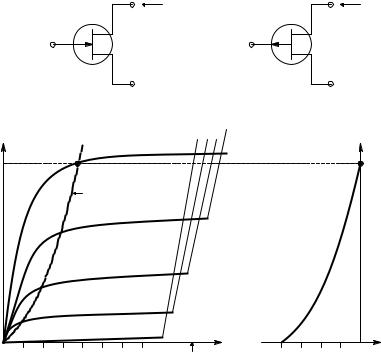
Figure 2.27 illustrates the symbols for n- and p-channel JFETs and the volt–ampere curves for an n-channel JFET. Note that the gate-to-channel pn junction is normally reverse-biased in a JFET; thus, the gate current is the reverse saturation current of this diode (Irs), which is on the order of nA. In the n-channel JFET, all the currents and voltages are positive as written, with vGS being negative. In the p-channel JFET, all the signs are reversed: iD and vDS are negative and vGS is positive. The operating region of the JFET’s (iD, vDS) curves is ohmic to the left of the IDB line and saturated to the right of the IDB line.
|
|
|
|
|
D |
iD |
D |
|
|
iD |
|
|
|
|
|
+ |
|
+ |
|
|
|
|
|
|
G |
|
vDS |
G |
|
|
vDS |
|
|
|
|
|
|
|
|
|
|||
|
|
|
+ |
|
|
|
+ |
|
|
|
|
|
|
|
vGS |
− |
|
vGS |
|
|
− |
|
|
|
|
|
|
|
|
|
||
|
|
|
|
|
− |
|
|
− |
|
|
|
|
|
|
|
S |
|
|
|
S |
|
|
|
|
|
|
n-channel |
|
|
p-channel |
||
iD |
|
|
|
|
vGS = 0 |
|
|
|
|
iD |
|
|
|
|
|
|
|
|
|
|
|
IDSS |
|
|
|
|
|
|
|
|
|
IDSS |
|
|
|
|
|
IDB = IDSS (VDS /VP)2 |
|
|
|
||
|
|
|
|
|
vGS = −1 V |
|
vDS > vGS + vP |
|||
|
|
|
|
|
|
|
||||
|
|
|
|
|
vGS = −2 V |
|
|
|
|
|
|
|
|
|
|
vGS = −3 V |
|
|
|
|
|
|
|
|
vGS = VP = −4 V |
|
vDS |
|
|
vGS |
||
0 |
2 |
4 |
6 |
8 10 12 14 |
|
−4 |
−3 |
−2 |
0 |
|
|
|
−1 |
||||||||
|
|
|
|
|
|
|
BVGD |
|
|
|
FIGURE 2.27
Top: symbols for n- and p-channel JFETs. Bottom left: iD vs. vDS curves for an n-channel JFET. Area to left of IDB parabola has ohmic FET operation; area to right of IDB line has saturated (channel) operation. Bottom right: the iD vs. vGS curve for saturated operation [vDS > ΩvGS + VPΩ]. The pinch-off voltage VP = −4 V in this example.
© 2004 by CRC Press LLC

58 |
|
|
Analysis and Application of Analog Electronic Circuits |
||||||
|
|
D |
|
|
|
|
|
|
D |
|
|
|
|
|
|
|
|
|
|
|
iD |
+ |
G |
D |
|
G |
|
id |
|
|
|
|
|
+ |
|||||
|
|
|
|
|
|
|
|
rd |
|
|
|
|
|
|
|
|
|
|
|
G |
|
|
+ gmvgs |
id |
+ |
+ |
− |
|
|
|
|
vDS |
|
|
|
|
vds |
||
|
|
|
|
|
|
|
|||
+ |
|
|
vgs |
gd vds |
vgs µvgs |
|
|
||
vGS |
− |
− |
− |
− |
|
− |
+ |
|
− |
|
|
|
|
||||||
|
|
|
|
|
|
|
|
|
|
|
|
S |
S |
S |
|
S |
|
|
S |
FIGURE 2.28
Left: symbol for n-channel JFET. Center: Norton MFSSM for p- and n-channel JFETs. Right: Thevenin MFSSM for JFETs.
Just as there is a mathematical model for pn junction diode current, there is also a mathematical approximation to JFET behavior in the saturation region. This is:
ID = IDSS (1− VGS VP )2 for VDS > |
|
VGS + Vp |
|
and |
|
VGS |
|
< |
|
VP |
|
(2.69) |
|
|
|
|
|
|
|||||||
|
|
|
|
|||||||||
|
|
|
|
|
|
|
|
|
|
|
|
|
In the ohmic region, ID is modeled by:
ID = IDSS[2(1+ VGS  VP )(VDS
  VP )− (VDS
  VP )2 ] for 0 < VDS < VGS + Vp (2.70)
For VGS VP,
ID = IDSS[2(1+ VGS VP )(VDS VP )] |
(2.71) |
where IDSS is the drain current defined for VGS = 0 and VDS > VGS + VP . VP is the pinch-off voltage, i.e., VP = VGS where ID 0, given VDS > VGS + VP . In the ohmic region, the JFET behaves like a voltage-controlled conductance:
gd = |
∂iD |
|
VGS = IDSS[2(1+ (VGS VP )) VP ] |
(2.72) |
|
||||
∂vDS |
||||
In the saturation region, n- and p-channel JFETs have the same MFSSM, shown in Figure 2.28. The transconductance of the VCCS is defined by:
g |
|
= |
∂iD |
|
Q,V = const. |
(2.73) |
|
m |
∂vDS |
||||||
|
|
GS |
|
||||
|
|
|
|
|
|||
By differentiating Equation 2.69, an algebraic expression is found for gm:
gm = |
2 |
IDSS |
(1− VGS VP ) |
(2.74) |
|
|
V |
|
|||
|
|
P |
|
|
|
© 2004 by CRC Press LLC
Models for Semiconductor Devices Used in Analog Electronic Systems |
59 |
|
Note from Equation 2.69 that |
ID can be written as: |
|
ID = |
IDSS (1− VGS VP ) |
(2.75) |
Now Equation 2.75 can be substituted into Equation 2.74 to find:
gm = |
2IDSS |
|
IDQ |
= gmo |
IDQ |
for VDS > |
|
VGS + VP |
|
(2.76) |
||||
|
|
|
||||||||||||
|
V |
|
|
I |
DSS |
I |
DSS |
|
|
|||||
|
|
|
|
|
|
|||||||||
|
|
P |
|
|
|
|
|
|
|
|
|
|
||
Equation 2.76 gives an algebraic means of estimating a JFET’s gm in terms of its quiescent drain current (IDQ) and the manufacturer-specified parameters, IDSS and VP. gmo is the JFET’s (maximum) transconductance at VGS = 0
and VDS > VGS + VP .
The MFSSM for a saturated-channel JFET is also characterized by an output conductance in parallel with the VCCS. This small-signal conductance is due in part to the upward slope of the iD = f(vGS, vDS) curve family :
gd = |
∂iD |
|
|
= |
ID |
|
|
Siemens |
(2.77) |
∂vDS |
|
VGS |
VDS |
|
Q,VGS = const. |
||||
|
|
|
|
|
|
||||
|
|
|
|
|
|
To model the upward slope of the iD = f(vGS, vDS) curve family, we choose a voltage Vx such that:
ID IDSS (1− VGS  VP )2 (1− VDS
  Vx ) for VDS > VGS + VP and VGS < VP (2.78)
Note that the intercept voltage, Vx, is typically 25 to 50 V in magnitude. Vx is negative and VDS is positive for n-channel JFETs and Vx is positive and VDS is negative for p-channel JFETs. An algebraic expression for gd can be found by differentiating Equation 2.78.
|
|
∂ID |
|
|
2 |
(−1 Vx ) = −(IDQ |
Vx )> 0 |
|
gd |
= |
|
|
|
= IDSS (1− VGS VP ) |
(2.79) |
||
∂VDS |
|
Q |
||||||
|
|
|
|
|
|
|
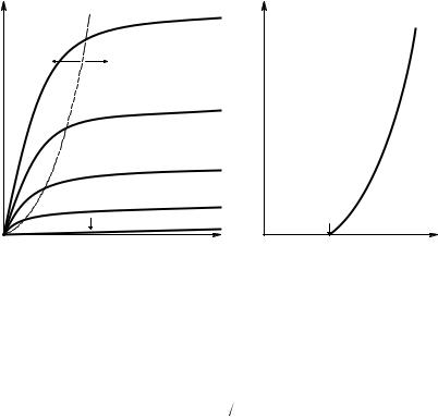
An estimate of Vx can be found by extrapolating the iD = f(vGS, vDS) curves in the saturation region back to the negative VSD axis, as shown in Figure 2.29.
The Norton drain–source model shown in Figure 2.28 can be made into a Thevenin model in which the series Thevenin resistance is just rd = 1/gd and the open-circuit voltage is given by a VCVS, μvGS. (Note the sign of the VCVS; it is the same for n- and p-channel JFETs.
The voltage gain, μ, is easily seen to be given by:
© 2004 by CRC Press LLC

60 |
Analysis and Application of Analog Electronic Circuits |
 iD
iD
vGS = 0
vGS = −1
vGS = −2
vGS = −3
vGS = −4 = VP
Vx |
0 |
iD |
gm |
IDSS |
gmo |
vGS |
vGS |
0 |
0 |
VP |
VP |
vDS
gd |
IDSS /Vx |
|
|
|
iDQ |
0 |
IDSS |
|
FIGURE 2.29
Top: large-signal iD vs. vDS curves for an n-channel JFET showing the geometry of the FET equivalent of the BJT Early voltage, Vx. Bottom, left to right: small-signal iD vs. vGS for a saturated channel. Small-signal gm vs. vGS for a saturated channel. Small-signal Norton drain conductance, gd vs. iD for a saturated channel.
μ = gm gd = gmo |
(IDQ |
IDSS )( |
|
Vx |
IDQ |
|
)= |
gmo |
Vx |
|
(2.80) |
||
|
|
|
|||||||||||
|
|
I |
DQ |
I |
DSS |
||||||||
|
|
|
|
|
|
|
|
|
|||||
|
|
|
|
|
|
|
|
|
|
|
|||
In the saturation region of operation, μ varies inversely with IDQ. Either the Norton or Thevenin model is valid. Most engineers use the Norton model because manufacturers generally provide VP, IDSS, and gmo for a given JFET.
2.4.3MOSFET Behavior at Mid-Frequencies
MOSFETS are also known as insulated gate field-effect transistors (IgFETS). The gate electrode is insulated from the channel, thus gate leakage current is on the order of picoamperes or less. Symbols for n-channel, p-channel, and the iD = f(vGS, vDS) curves for an n-channel depletion MOSFET are shown
© 2004 by CRC Press LLC

Models for Semiconductor Devices Used in Analog Electronic Systems |
61 |
|||||||
|
|
|
D |
|
D |
|
|
|
|
|
|
+ |
|
|
|
+ |
|
|
G |
|
|
G |
|
|
|
|
|
|
|
vDS |
|
|
|
vDS |
|
|
+ |
|
|
+ |
|
|
|
|
|
vGS |
− |
− |
− |
vGS |
− |
|
|
|
|
|
|
|
||||
|
A |
S |
B |
|
S |
|
||
|
|
|
|
|
||||
|
|
|
|
|
|
|
||
iD |
|
VGS = +1 |
|
|
|
iD |
|
|
|
|
|
|
|
|
|
||
|
VDS > VGS + VP |
|
|
|
|
|
||
IDSS |
|
|
VGS = 0 |
|
|
|
IDSS |
|
|
|
|
|
|
|
|
||
|
|
|
VGS = −1 |
|
|
|
|
|
|
|
|
VGS = −2 |
|
|
|
|
|
|
|
|
VGS = VP = −3 V |
vDS |
|
|
|
vGS |
|
|
|
|
|
|
|
|
|
0 |
|
|
0 |
|
VP −2 −1 |
|
+1 |
|
|
|
|
|
|
|
|
||
|
C |
|
|
D |
|
|
|
|
FIGURE 2.30
(A) Symbol for an n-channel MOSFET. (B) Symbol for a p-channel MOSFET. (C) The iD = f(vGS, vDS) curves for an n-channel depletion MOSFET. (D) The iD = f(vGS) curve for a saturated-channel, n-channel depletion MOSFET.
in Figure 2.30. In the depletion device, a lightly doped p-substrate underlies a lightly doped n-channel connecting two heavily doped n-regions for the source and drain. This device has a negative pinch-off voltage (VP); however,
ID = IDSS when VGS = 0 and the saturated channel conducts heavily for VGS > 0. Similar to the n-channel JFET, it is possible to model the iD = f(vGS, vDS)
curves of the depletion n-channel MOSFET in the saturation region by:
iD = IDSS[1− (vGS VP )]2 |
for vDS > |
|
vGS + VP |
|
> 0 |
(2.81) |
|
|
and in the ohmic region:
iD = IDSS[2(1+ vGS  VP )(vDS
  VP )− (vDS
  VP )2 ] for 0 < vDS < vGS + VP (2.82)
When the iD = f(vGS, vDS) curves of the enhancement n-channel MOSFET shown in Figure 2.31 are considered, it can be seen that there is no IDSS for this family of device. Channel cut-off occurs at a threshold voltage, vGS = VT,
© 2004 by CRC Press LLC
62 |
Analysis and Application of Analog Electronic Circuits |
|||
iD |
|
|
iD |
|
|
vGS = +7 V |
|
|
|
Ohmic |
Saturation region |
|
|
|
region |
|
|
|
|
|
|
|
|
|
|
vGS = +6 V |
|
|
|
|
vGS = +5 V |
|
|
|
|
vGS = +4 V |
|
|
|
|
vGS = VT = +3 V |
|
VT |
vGS |
|
|
|
||
0 |
v |
DS |
0 1 2 3 4 5 6 7 |
|
FIGURE 2.31
Left: the iD = f(vGS, vDS) curves for an n-channel enhancement MOSFET. Right: the iD = f(vGS) curve for a saturated-channel, n-channel enhancement MOSFET.
where iD reaches some defined low value, e.g., 10 μA. The mathematical model for n-channel enhancement MOSFET iD = f(vGS, vDS) in the saturation region is:
iD = K(vGS − VT )2 = K VT2 (1− vGS VT )2 |
for 0 < |
|
vGS − VT |
|
< |
|
vDS |
|
(2.83) |
||||||||
|
|
|
|
||||||||||||||
In the ohmic channel operating region: |
|
|
|
|
|
|
|
|
|
|
|
|
|
|
|
|
|
iD = K[2(vGS − VT )vDS − vDS2 ] for |
0 < |
|
vDS |
|
< |
|
vGS − VT |
|
|
(2.84) |
|||||||
|
|
|
|
||||||||||||||
The line separating the saturatedand ohmic-channel regions is |
|
|
|||||||||||||||
IDB = K VDS2 |
|
|
|
|
|
|
|
|
|
|
|
|
|
|
|
(2.85) |
|
p-channel MOSFETs have iD = f(vGS, vDS) curves with the signs opposite those for n-channel devices. It is easy to see from Equation 2.73, which defines the small-signal transconductance, and Equation 2.72, which defines the small-signal drain conductance, that all FETs (JFETs, MOSFETs, n-channel, p-channel, enhancement, depletion) have the same parsimonious MFSSM — a case of electronic serendipity.
2.4.4Basic Mid-Frequency Single FET Amplifiers
Just as in the case of BJTs, there are so-called grounded-source amplifiers, grounded-gate amplifiers, and source followers. In order to find the small-
© 2004 by CRC Press LLC
Models for Semiconductor Devices Used in Analog Electronic Systems |
63 |
VDD
|
|
|
|
RD |
|
|
|
D |
vo |
|
C1 |
G |
|
|
|
|
|
||
|
|
|
|
|
|
|
+ |
|
|
+ |
|
vgs |
|
S |
|
− |
|
||
|
|
|
|
v1
RG RS CS
−
A
|
G |
D |
vo |
|
|
|
|
|
+ |
|
|
v1 |
RG |
gd |
GD |
|
− |
gmvgs |
|
|
S |
|
|
|
|
|
B
FIGURE 2.32
(A) An n-channel JFET “grounded-source” amplifier. CS bypasses small ac signals at the JFET’s source to ground, making vs = 0. (B) MFSSM of the amplifier. The same MFSSM would obtain if a p-channel JFET were used.
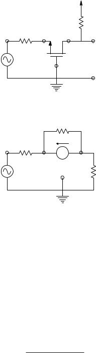
signal voltage gain of each if these amplifiers, as well as their input and output resistances, first examine a JFET grounded-source amplifier, shown in Figure 2.32. At mid-frequencies, the external coupling and bypass capacitors are treated as short circuits. Thus, the source is at small-signal ground, so vs = 0. The amplifier’s mid-frequency gain is found from the node equation:
vo [GD + gd] = –gm vgs = –gm v1 |
(2.86) |
|||||||
|
|
|
|
¬ |
|
|
|
|
K |
|
= |
vo |
= |
−gmrdRD |
|
(2.87) |
|
v |
v1 |
RD + rd |
||||||
|
|
|
|
|||||
|
|
|
|
|
||||
From inspection of the MFSSM of the circuit, Rin • and Rout = RD rd/(RD + rd).
© 2004 by CRC Press LLC
64 |
Analysis and Application of Analog Electronic Circuits |
VDD
RD
RS vs D
vo
S
+
v1
G
A
|
|
gd |
|
|
gmvgs |
|
RS vs |
vo |
|
|
|
+ |
S |
D |
|
|
|
v1 |
|
RD |
|
|
G |
B
FIGURE 2.33
(A) An n-channel MOSFET grounded-gate amplifier. (B) MFSSM of the MOSFET G-G amplifier. See text for analysis.
Next, consider an n-channel MOSFET grounded-gate amplifier at midfrequencies. The electrical circuit and its MFSSM are shown in Figure 2.33. Write two node equations, one for the vs node and the other for the drain (output) node.
vs [GS + gd + gm] − vo [gd] = v1GS
−vs [gd + gm] + vo [gd + GD] = 0
Using Cramer’s rule:
= GS gd + GD [GS + gd + gm]
vs = |
RD + rd |
|
v1 |
|
RD + rd + RS (1+ gmrd ) |
(2.88A)
(2.88B)
(2.89)
(2.90)
© 2004 by CRC Press LLC

Models for Semiconductor Devices Used in Analog Electronic Systems |
65 |
|||||
|
vo |
= |
RD (1+ gmrd ) |
= K |
|
(2.91) |
|
|
RD + rd + RS (1+ gmrd ) |
v |
|||
|
v1 |
|
|
|||
|
|
|
|
|||
The input resistance, Rin, of the MOSFET GG amplifier is found from:
|
v1 |
|
v1RS |
|
|
|
RS |
|
|
|
RD + rd |
|
|
Rin = |
|
= |
v1(1− vs v1) |
= |
|
|
|
|
|
|
= RS + |
(1+ gmrd ) |
(2.92) |
is |
1− |
|
|
RD |
+ rd |
|
|||||||
|
|
|
RD |
+ rd |
+ RS (1+ gmrd ) |
|
|||||||
|
|
|
|
|
|
|
|
|
|
||||
Rout is approximately RD for the GG amplifier.
Finally, examine the MOSFET source-follower amplifier at mid-frequen- cies. The circuit and its MFSSM are shown in Figure 2.34. This an easy circuit to analyze because the drain is at SS ground. The output node equation is:
vo [GC + gd + gm] = gm v1 |
(2.93) |
Equation 2.93 leads to the SF amplifier’s gain:
K |
|
= |
vo |
= |
RD gmrd |
< 1 |
(2.94) |
|
v |
v1 |
rd + RD (1+ gmrd ) |
||||||
|
|
|
|
|
||||
|
|
|
|
|
|
By inspection, Rin •; Rout can be found by voc/isc.
|
|
|
v1RD gmrd |
|
|
|
R = |
voc |
= |
rd + RD (1+ gmrd ) |
= |
RD rd (1+ gmrd ) |
(2.95) |
|
|
RD + rd (1+ gmrd ) |
||||
out |
isc |
|
gmv1 |
|
||
|
|
|
||||
Single FET amplifiers generally have higher Rin, about the same Rout, less gain, and more even harmonic distortion than equivalent BJT amplifiers.
2.4.5Simple Amplifiers Using Two FETs at Mid-Frequencies
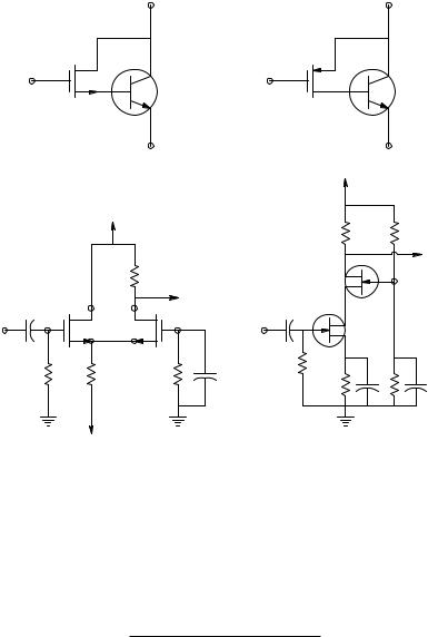
As in the case of BJTs, certain basic building blocks for analog ICs can be made from two transistors. Figure 2.35 illustrates four such circuits using field-effect transistors. Notably absent is the difference amplifier; because of its great importance in analog electronic circuits, the DA is treated separately in Chapter 3 of this text. Figure 2.35(A) illustrates a Darlington amplifier in which the input transistor is an n-channel MOSFET acting as a voltage control-led current source driving the base of a power npn BJT. Figure 2.35(B) shows the FET–BJT equivalent for the “feedback pair” power amplifier. In Figure 2.35(C), a source-follower/grounded-gate high-frequency amplifier can be seen and an FET–FET cascode amplifier is shown in Figure 2.35(D).
© 2004 by CRC Press LLC

66 |
Analysis and Application of Analog Electronic Circuits |
−VDD
|
|
D |
|
|
G |
|
|
|
+ |
|
|
+ |
vgs S |
|
|
− |
|
||
|
+ |
||
v1 |
RG |
||
RS vo |
|||
− |
|
||
|
− |
||
|
|
A
|
|
D |
|
gmvgs |
|
G |
+ |
gd |
|
|
|
+ |
vgs |
vo |
− S |
|
|
v1 |
RG |
|
− |
|
RS |
|
|
B
FIGURE 2.34
(A) A p-channel MOSFET source follower. (B) MFSSM for the MOSFET S-F.
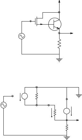
It is necessary first to examine the gain of the FET–BJT Darlington connected as an emitter follower. This circuit and its MFSSM are shown in Figure
2.36. Analysis begins by writing the node equations for the vs and vo nodes; |
|
note that ib = gie (vs − vo); vgs = v1 − vs; μ = gm rd; and gie = 1/hie. |
|
vs [gd + gie + gm] − vo gie = v1 gm |
(2.96A) |
−vs [gie (1 + hfe)] + vo [gie (1 + hfe) + GE] = 0 |
(2.96B) |
Using Cramer’s rule, |
|
= (gd + gm)gie (1 + hfe) + GE (gd + gie + gm) |
(2.97) |
vo = v1 gm gie (1 + hfe) |
(2.98) |
© 2004 by CRC Press LLC
Models for Semiconductor Devices Used in Analog Electronic Systems |
67 |
Q1 |
D |
Q2 |
|
|
|
Q1 S |
Q2 |
|
|
|
|
|
|
||||
G |
|
G |
|
|
V1 |
|
|
|
V1 |
vs |
|
|
|
vd |
|
|
|
|
S |
|
|
|
|
D |
|
|
|
A |
|
|
|
B |
|
|
|
|
|
|
|
|
|
|
VDD |
|
|
|
VDD |
|
|
|
|
|
|
|
|
|
|
|
|
|
Rd |
|
|
|
|
|
|
|
D |
|
Vo |
|
|
|
|
|
|
|
|
|
|
|
Rd |
|
|
|
|
|
(0) |
|
|
|
|
|
|
|
|
|
|
Q1 |
|
Vo |
|
|
S |
|
|
|
|
|
|
vs |
Q2 |
|
||
|
|
|
|
|
|
|
||
G |
D |
D |
(0) |
|
|
Q1 |
D |
|
|
|
|
|
|
||||
V1 |
|
vs |
|
|
V1 |
|
|
|
|
|
|
|
|
|
|
S |
|
|
S |
S Q2 |
|
|
|
Rg |
|
|
Rg |
Rs |
|
Rg |
∞ |
|
|
|
|
|
|
|
∞ |
∞ |
||||
|
|
|
Rs |
|||||
|
|
|
|
|
|
|||
|
|
|
|
|
|
|
|
C D
FIGURE 2.35
(A) An n-channel MOSFET/npn BJT Darlington configuration. (B) A p-channel MOSFET/npn BJT feedback pair configuration. (C) An n-channel MOSFET source-follower–grounded-gate amplifier. (D) An n-channel JFET cascode amplifier.
Solving for vo/v1 yields:
vo |
= |
RE (1+ hfe )μ |
|
|
RE (1+ hfe )(1+ μ) + hie (1+ μ) + rd |
(2.99) |
|
v1 |
As expected, this voltage gain is <1. The amplifier’s input resistance is extremely high and the output resistance can be found by the open-circuit output voltage, given by Equation 2.99, divided by the short-circuit output
current, which is simply ib(1 + hfe) for vo = 0, (Rout = OCV/SCC). Rout is on the order of single ohms.
Next, find the gain for the FET–BJT feedback pair amplifier shown in Figure 2.35(B). The node equations are:
© 2004 by CRC Press LLC
68 |
Analysis and Application of Analog Electronic Circuits |
VCC
vo
v1
RE
D
gmvgs
gd
G
vs B
v1
S
ib hie hfe ib
vo
RE
FIGURE 2.36
Top: A MOSFET/BJT Darlington connected as an emitter-follower. Bottom: MFSSM of the Darlington EF. See analysis in text.
vd [gd + gie] − vo [gie] = − v1 gm |
(2.100A) |
−vd [gie (1 + hfe)] + vo [GE + gie (1 + hfe)] = 0 |
(2.100B) |
Using Cramer’s rule, |
|
= gd [GE + gie (1 + hfe)] + gie GE |
(2.101) |
vo = − v1 gm gie (1 + hfe) |
(2.102) |
from which the mid-frequency voltage gain is found:
© 2004 by CRC Press LLC

Models for Semiconductor Devices Used in Analog Electronic Systems |
69 |
|
RD |
|
vo |
D |
D |
gmvgs1 |
gmvgs2 |
gd |
gd |
G |
G |
|
vs |
v1 |
|
S |
S |
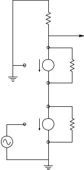
RS
FIGURE 2.37
MFSSM for the two-MOSFET SF/GG amplifier. See text for analysis.
vo |
= |
−REμ(1+ hfe ) |
= |
−μR |
|
|
|
RE (1+ hfe )+ hie + rd |
RE + (hie + rd )E (1+ hfe ) |
= Kv |
(2.103) |
||
v1 |
||||||
Again, Rin is very high because of the MOSFET and Rout can be found from
Rout = OCV/SCC. It can be shown that Rout is RE in parallel with (hie + rd)/(1 + hfe) ohms.
The MFSSM of the FET–FET SF-GG amplifier of Figure 2.35(C) is shown in Figure 2.37. Proceeding as before, write the node equations for vs and vo, then use Cramer’s rule to find the amplifier’s MFSS gain; note that vgs1 = v1 − vs and vgs2 = − vs.
vs [2(gd + gm) + GS] − vo [gd] = gm v1 |
(2.104A) |
−vs [gd + gm] + vo [GD + gd] = 0 |
(2.104B) |
= 2GD (gd + gm) + gd (gm + GS) + GS GD |
(2.105) |
vo = v1 gm (gd + gm) |
(2.106) |
The voltage gain is found from Equation 2.105 and Equation 2.106:
vo |
= |
+RDμ |
|
= K |
|
(2.107) |
|
v1 |
RD + 2rd + rd (rd + RD ) [RS |
(1+ μ)] |
v |
||||
|
|
|
|||||
|
|
|
|
|
|
© 2004 by CRC Press LLC
70 |
Analysis and Application of Analog Electronic Circuits |
RD
vo
D
gmvgs2
gd
G
S
vs
D
gmvgs1
gd
G
+
v1 |
S |
FIGURE 2.38
MFSSM for the two-JFET cascode amplifier. See text for analysis.
Note that the gain is noninverting; Rin is on the order of 1013 Ω and Rout is slightly lower than RD.
The final two-FET amplifier considered is the cascode amplifier using two JFETs shown in Figure 2.35(D). The MFSSM of the cascode is shown in Figure 2.38. Note that vgs1 = v1, vgs2 = −vs, the JFETs are matched, and μ = gm rd. The node equations are:
vs [2gd + gm] − vo gd = − gmv1 |
(2.108A) |
−vs [gd + gm] + vo [GD + gd] = 0 |
(2.108B) |
= 2gd GD + 2gd2 + gmGD + gm gd − gd2 − gm gd = GD(2gd + gm) + gd2 (2.109)
vo = − v1 gm [gd + gm] |
(2.110) |
The cascode amplifier’s mid-frequency voltage gain is found to be:
vo |
= |
−RDμ(1+ μ) |
= K |
|
(2.111) |
|
RD + rd (1+ μ) |
v |
|||
v1 |
|
|
|||
|
|
|
|
|
|
© 2004 by CRC Press LLC