

- •Analysis and Application of Analog Electronic Circuits to Biomedical Instrumentation
- •Dedication
- •Preface
- •Reader Background
- •Rationale
- •Description of the Chapters
- •Features
- •The Author
- •Table of Contents
- •1.1 Introduction
- •1.2 Sources of Endogenous Bioelectric Signals
- •1.3 Nerve Action Potentials
- •1.4 Muscle Action Potentials
- •1.4.1 Introduction
- •1.4.2 The Origin of EMGs
- •1.5 The Electrocardiogram
- •1.5.1 Introduction
- •1.6 Other Biopotentials
- •1.6.1 Introduction
- •1.6.2 EEGs
- •1.6.3 Other Body Surface Potentials
- •1.7 Discussion
- •1.8 Electrical Properties of Bioelectrodes
- •1.9 Exogenous Bioelectric Signals
- •1.10 Chapter Summary
- •2.1 Introduction
- •2.2.1 Introduction
- •2.2.4 Schottky Diodes
- •2.3.1 Introduction
- •2.4.1 Introduction
- •2.5.1 Introduction
- •2.5.5 Broadbanding Strategies
- •2.6 Photons, Photodiodes, Photoconductors, LEDs, and Laser Diodes
- •2.6.1 Introduction
- •2.6.2 PIN Photodiodes
- •2.6.3 Avalanche Photodiodes
- •2.6.4 Signal Conditioning Circuits for Photodiodes
- •2.6.5 Photoconductors
- •2.6.6 LEDs
- •2.6.7 Laser Diodes
- •2.7 Chapter Summary
- •Home Problems
- •3.1 Introduction
- •3.2 DA Circuit Architecture
- •3.4 CM and DM Gain of Simple DA Stages at High Frequencies
- •3.4.1 Introduction
- •3.5 Input Resistance of Simple Transistor DAs
- •3.7 How Op Amps Can Be Used To Make DAs for Medical Applications
- •3.7.1 Introduction
- •3.8 Chapter Summary
- •Home Problems
- •4.1 Introduction
- •4.3 Some Effects of Negative Voltage Feedback
- •4.3.1 Reduction of Output Resistance
- •4.3.2 Reduction of Total Harmonic Distortion
- •4.3.4 Decrease in Gain Sensitivity
- •4.4 Effects of Negative Current Feedback
- •4.5 Positive Voltage Feedback
- •4.5.1 Introduction
- •4.6 Chapter Summary
- •Home Problems
- •5.1 Introduction
- •5.2.1 Introduction
- •5.2.2 Bode Plots
- •5.5.1 Introduction
- •5.5.3 The Wien Bridge Oscillator
- •5.6 Chapter Summary
- •Home Problems
- •6.1 Ideal Op Amps
- •6.1.1 Introduction
- •6.1.2 Properties of Ideal OP Amps
- •6.1.3 Some Examples of OP Amp Circuits Analyzed Using IOAs
- •6.2 Practical Op Amps
- •6.2.1 Introduction
- •6.2.2 Functional Categories of Real Op Amps
- •6.3.1 The GBWP of an Inverting Summer
- •6.4.3 Limitations of CFOAs
- •6.5 Voltage Comparators
- •6.5.1 Introduction
- •6.5.2. Applications of Voltage Comparators
- •6.5.3 Discussion
- •6.6 Some Applications of Op Amps in Biomedicine
- •6.6.1 Introduction
- •6.6.2 Analog Integrators and Differentiators
- •6.7 Chapter Summary
- •Home Problems
- •7.1 Introduction
- •7.2 Types of Analog Active Filters
- •7.2.1 Introduction
- •7.2.3 Biquad Active Filters
- •7.2.4 Generalized Impedance Converter AFs
- •7.3 Electronically Tunable AFs
- •7.3.1 Introduction
- •7.3.3 Use of Digitally Controlled Potentiometers To Tune a Sallen and Key LPF
- •7.5 Chapter Summary
- •7.5.1 Active Filters
- •7.5.2 Choice of AF Components
- •Home Problems
- •8.1 Introduction
- •8.2 Instrumentation Amps
- •8.3 Medical Isolation Amps
- •8.3.1 Introduction
- •8.3.3 A Prototype Magnetic IsoA
- •8.4.1 Introduction
- •8.6 Chapter Summary
- •9.1 Introduction
- •9.2 Descriptors of Random Noise in Biomedical Measurement Systems
- •9.2.1 Introduction
- •9.2.2 The Probability Density Function
- •9.2.3 The Power Density Spectrum
- •9.2.4 Sources of Random Noise in Signal Conditioning Systems
- •9.2.4.1 Noise from Resistors
- •9.2.4.3 Noise in JFETs
- •9.2.4.4 Noise in BJTs
- •9.3 Propagation of Noise through LTI Filters
- •9.4.2 Spot Noise Factor and Figure
- •9.5.1 Introduction
- •9.6.1 Introduction
- •9.7 Effect of Feedback on Noise
- •9.7.1 Introduction
- •9.8.1 Introduction
- •9.8.2 Calculation of the Minimum Resolvable AC Input Voltage to a Noisy Op Amp
- •9.8.5.1 Introduction
- •9.8.5.2 Bridge Sensitivity Calculations
- •9.8.7.1 Introduction
- •9.8.7.2 Analysis of SNR Improvement by Averaging
- •9.8.7.3 Discussion
- •9.10.1 Introduction
- •9.11 Chapter Summary
- •Home Problems
- •10.1 Introduction
- •10.2 Aliasing and the Sampling Theorem
- •10.2.1 Introduction
- •10.2.2 The Sampling Theorem
- •10.3 Digital-to-Analog Converters (DACs)
- •10.3.1 Introduction
- •10.3.2 DAC Designs
- •10.3.3 Static and Dynamic Characteristics of DACs
- •10.4 Hold Circuits
- •10.5 Analog-to-Digital Converters (ADCs)
- •10.5.1 Introduction
- •10.5.2 The Tracking (Servo) ADC
- •10.5.3 The Successive Approximation ADC
- •10.5.4 Integrating Converters
- •10.5.5 Flash Converters
- •10.6 Quantization Noise
- •10.7 Chapter Summary
- •Home Problems
- •11.1 Introduction
- •11.2 Modulation of a Sinusoidal Carrier Viewed in the Frequency Domain
- •11.3 Implementation of AM
- •11.3.1 Introduction
- •11.3.2 Some Amplitude Modulation Circuits
- •11.4 Generation of Phase and Frequency Modulation
- •11.4.1 Introduction
- •11.4.3 Integral Pulse Frequency Modulation as a Means of Frequency Modulation
- •11.5 Demodulation of Modulated Sinusoidal Carriers
- •11.5.1 Introduction
- •11.5.2 Detection of AM
- •11.5.3 Detection of FM Signals
- •11.5.4 Demodulation of DSBSCM Signals
- •11.6 Modulation and Demodulation of Digital Carriers
- •11.6.1 Introduction
- •11.6.2 Delta Modulation
- •11.7 Chapter Summary
- •Home Problems
- •12.1 Introduction
- •12.2.1 Introduction
- •12.2.2 The Analog Multiplier/LPF PSR
- •12.2.3 The Switched Op Amp PSR
- •12.2.4 The Chopper PSR
- •12.2.5 The Balanced Diode Bridge PSR
- •12.3 Phase Detectors
- •12.3.1 Introduction
- •12.3.2 The Analog Multiplier Phase Detector
- •12.3.3 Digital Phase Detectors
- •12.4 Voltage and Current-Controlled Oscillators
- •12.4.1 Introduction
- •12.4.2 An Analog VCO
- •12.4.3 Switched Integrating Capacitor VCOs
- •12.4.6 Summary
- •12.5 Phase-Locked Loops
- •12.5.1 Introduction
- •12.5.2 PLL Components
- •12.5.3 PLL Applications in Biomedicine
- •12.5.4 Discussion
- •12.6 True RMS Converters
- •12.6.1 Introduction
- •12.6.2 True RMS Circuits
- •12.7 IC Thermometers
- •12.7.1 Introduction
- •12.7.2 IC Temperature Transducers
- •12.8 Instrumentation Systems
- •12.8.1 Introduction
- •12.8.5 Respiratory Acoustic Impedance Measurement System
- •12.9 Chapter Summary
- •References

304 |
Analysis and Application of Analog Electronic Circuits |
used to adjust synchronization signal phase in lock-in amplifiers and synchronous rectifiers, and to correct for phase lags inherent in data transmission on coaxial cables and other transmission lines.
7.5Chapter Summary
7.5.1Active Filters
There are many op amp active filter architectures. Some are easier to use in designing than others. This chapter focused on the easy ones: the controlledsource Sallen and Key filters; the biquad active filter family; and filters based on the generalized impedance converter circuit (GIC). Also covered were the design and analysis of electronically tunable active filters using variable-gain elements such as analog multipliers, multiplying DACs, digitally controlled potentiometers, and digitally controlled gain amplifiers. Electronically tuned filters have application as anti-aliasing filters and tuned filters that can track a coherent signal’s frequency — to compensate for Doppler shift, for example.
Although not covered in this chapter, a family of active filters called switched-capacitor filters (SCFs) are primarily used in telecommunications. The SCFs use MOS switches to commute capacitors in what would otherwise be an op amp, R–C filter design. The switched capacitor can be shown to emulate a resistor of value Req = Tc/Cs, where Tc is the period of the commutation and Cs is the switched capacitor value. The interested reader can consult Section 9.2 in Northrop (1990).
7.5.2Choice of AF Components
Because most analog AFs used in biomedical applications operate on signals in the 0- to 5-kHz range, overall filter high-frequency response is often not an important consideration. Instead, concern is with noise, linearity, dc drift, and stability of parameter settings (dc gain, ωn, and damping, ξ). To minimize noise and maximize parameter stability, metal film resistors (or wire-wound resistors) with low tempcos are generally chosen.
Choice of capacitors is important in determining filter linearity. Some capacitor dielectrics exhibit excessive losses, unidirectional dc leakage, and dielectric hysteresis; thus they can distort filtered signals. In particular, electrolytic and tantalum dielectric capacitors are not recommended for AF components; they are usually used for bypassing applications where they are operated with a fixed dc voltage bias. Polycarbonate dielectric capacitors can also distort signals. The best capacitor dielectrics are air, mica, ceramic, oiled paper, and mylar. Again, low tempcos are desired. Do not be tempted to use electrolytic or tantalum capacitors in an AF design that requires large capacitor values in order to realize a low ωn. Instead, use a GIC design for the filter that uses smaller Cs.
© 2004 by CRC Press LLC
Analog Active Filters |
305 |
Op amps used in AFs also must be chosen for dc stability (low offset voltage tempco), low noise, and high dc gain. Filters used at high frequencies (>10 kHz) generally require op amps with appropriately high fTs. All highfrequency filters should be simulated with an electronic circuit analysis program such as MicroCap or a flavor of SPICE‘ to ensure that no surprises will occur at high frequencies.
Home Problems
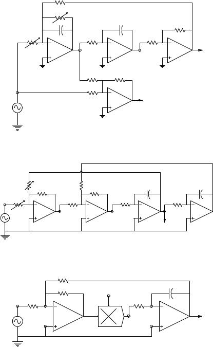
7.1The active filter circuit of Figure P7.1 is a version of a notch (band reject) filter. Assume the op amps are ideal.
a.Find an expression for the transfer function of the filter in timeconstant form. Let RC = τ.
b.Find the β value that will make the filter an ideal notch filter, i.e., put conjugate zeros exactly on the jω axis. Give an expression for the center frequency of the notch. What is the dc gain of the filter?
c.Now make the op amps be TI TL072. Use an ECAP to simulate
the frequency response of the notch filter. Set the notch frequency to 60 Hz. Use the ideal β value. Explain why the notch does not go to −• at 60 Hz. At what frequencies is the filter down −3 dB?
|
|
|
C |
|
100 kΩ |
|
|
R |
|
33.33 kΩ |
|
C |
R |
|
IOA |
V2 |
|
IOA |
Vo |
V1
βV2
FIGURE P7.1
7.2Consider the Sallen and Key high-pass filter shown in text Figure 7.3.
a.Design an HPF with pass-band gain of unity, fn = 100 Hz, and ξ = 0.707. Use a TL071 op amp. Specify circuit parameters.
b.Use an ECAP Bode plot to verify your design. Give the −3-dB frequencies of the filter and its highand low-frequency fTs.
7.3Derive an expression for the transfer function of the active filter of Figure P7.3 in time constant form. Give expressions for the filter’s ωn, dc gain, and damping factors of the numerator and denominator.
© 2004 by CRC Press LLC

306 |
Analysis and Application of Analog Electronic Circuits |
C
4R
R
C Vi’
 Vo
Vo
R Vi
V1 |
R |
FIGURE P7.3
7.4Design a band-pass filter for neural spike signal conditioning using two
cascaded quadratic Sallen and Key active filters (1 LP, 1 HiP) with the
following specifications: mid-band gain = 0 dB; −3 dB fLO = 300 Hz; ξLO = 0.5; −3 dB fHI = 4 kHz; and ξHI = 0.5. (Note that the filter −3dB-frequencies
are not necessarily their fns.) Use OP-27 op amps. Specify the R and C values. Note: all Rs must be between 103 and 106 Ω and C values must lie between 3 pF and 3 μF. Verify your design with a PSpice or MicroCap Bode plot.
7.5Design a quadratic GIC band-pass filter for geophysical applications to condition a seismometer output having fn = 1 Hz and Q = 10. Verify your design with a Bode plot done with MicroCap or PSpice. Use the same ranges of Rs and Cs as in the preceding problem.
7.6For the three-op amp biquad AF shown in Figure P7.6
a.Write the transfer function, V4/V1 in time-constant form.
b.Write the transfer function, V2/V1, for the AF in TC form. Give expressions for ωn, Q, and V2/V1 at ωn.
c.Write an expression for the transfer function, V5/V1, in time
constant form. Use an ECAP to make a Bode plot of V5/V1. Let R = 1 kΩ; R1 = 10 kΩ; R4 = 1 kΩ; and C = 10 nF. Op amps are TL074s.
7.7Find an expression for V4/V1 in time-constant form for the biquad AF shown in Figure P7.7. Give expressions for ωn, Q and V4/V1 at ωn. Assume ideal op amps.
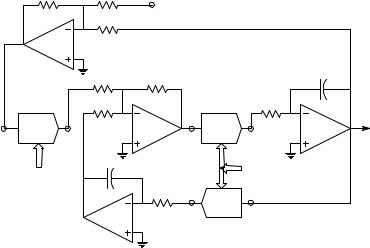
7.8Figure P7.8 illustrates a voltage-tunable, 1-pole LPF. An analog multiplier is used as the variable-gain element (VGE). The analog multiplier output V3 =
–V2Vc./10.
a.Derive an expression for Vo/V1 in time-constant form.
b.Make a dimensioned Bode plot of Vo/V1. Give expressions for the dc gain and the break frequency.
© 2004 by CRC Press LLC
Analog Active Filters |
|
|
|
307 |
|
R |
|
|
|
|
R1 |
|
|
|
|
C |
C |
|
R |
|
|
|
|
|
R4 |
|
R |
R |
|
|
|
V2 |
V3 |
V4 |
R R
R
V5
V1
FIGURE P7.6
R4 |
R |
|
|
R |
R |
C |
C |
R1 |
R |
R |
R |
V2 |
|
V3 |
V5 |
V1 |
|
|
V4 |
|
|
|
P7.7
FIGURE P7.7
R3 |
|
|
|
|
|
|
R2 |
|
Vc (dc) |
|
C |
|
|
|
|
|
|
|
||
R1 |
|
|
|
|
R4 |
|
|
V2 |
− |
+ |
|
|
|
IOA |
|
I |
OA |
Vo |
||
|
|
|||||
V1 |
|
|
|
|
−V2Vc /10 |
|
AM
FIGURE P7.8
© 2004 by CRC Press LLC

308 |
Analysis and Application of Analog Electronic Circuits |
||||
|
|
|
Vc (dc) |
|
|
|
R3 |
−V2Vc /10 |
+ |
|
|
|
− |
|
|
||
|
R2 |
|
C |
|
|
|
|
AM |
|
||
|
|
|
|
|
|
|
R1 |
|
|
R4 |
|
|
IOA |
|
I |
OA |
V2 |
|
V1 |
|
|
|
|
Vo
FIGURE P7.9
7.9Figure P7.9 illustrates another voltage-tuned active filter.
a.Derive an expression for Vo/V1 in time-constant form.
b.Make a dimensioned Bode plot of Vo/V1. Give expressions for the dc gain and the break frequency.
7.10The circuit of Figure P7.10 is an op amp AF realization of a Dolby B‘ audio noise reduction system recording encoder. It is designed to boost the highfrequency response of magnetic tape-recorded signals containing little power at high frequencies in order to improve playback signal-to-noise ratio (when used in conjunction with a Dolby B™ decoder filter). (Magnetic tape has an omnipresent high-frequency background “hiss” on playback, regardless of signal strength.)
a.Derive an expression for Vo/V1 in time-constant form.
b.Make a dimensioned Bode plot of Vo/V1. Give expressions for the dc gain and the break frequencies.
|
|
R |
|
|
|
|
C1 |
R |
R |
Vc > 0 |
|
C2 |
|
|
|
|
|
|
|
|
|
R |
R |
|
R/10 |
|
|
|
|
V3 |
+ |
|
|
|
|
IOA |
IOAI |
− |
V4 |
OA |
Vo |
V1 |
|
V2 |
AM |
|
|
|
|
|
|
|
|
|
FIGURE P7.10
© 2004 by CRC Press LLC

Analog Active Filters |
309 |
7.11The circuit of Figure P7.11 is an op amp AF realization of a Dolby B‘ audio noise reduction system decoder. It is designed to attenuate the high-frequency response of recorded signals containing high frequencies in order to improve playback signal-to-noise ratio (when used in conjunction with a Dolby B encoder filter).
a.Derive an expression for Vo/V1 in time-constant form.
b.Make a dimensioned Bode plot of Vo/V1. Give expressions for the dc gain and the break frequencies.
|
|
R |
C2 |
|
R1 |
Vc > 0 |
|
R |
|
|
|
|
|
|
C1 |
|
R |
|
|
V2 |
+ |
|
|
|
IOA |
− |
V3 I |
OA |
Vo |
V1
AM
FIGURE P7.11
7.12The circuit of Figure P7.12 is a digitally tunable biquad band-pass filter. MDACs are used as variable gain elements (VGEs). The analog input signal to the MDAC is multiplied by a fraction determined by the digital word input to the MDAC. For example, for MDAC1, its output is the analog signal:
|
|
N |
|
|
|
|
|
D |
2k−1 |
V |
= V |
1k |
|
|
|
|
|||
3 |
2 2N |
|
||
where N is the number of binary bits in the word, D1k = 0,1; for N = 8, the maximum gain is 255/256 (All D1k = 1) and the minimum gain is 0/256 (all D1k = 0).
a.Find the transfer function, (Vo/V1)(s) in Laplace format.
b.Give expressions for the filter’s ωn, Q, and peak gain in terms of {D1k}, {D2k}, and system parameters. What is the range of Q? Assume N = 8 bits and the op amps are ideal.
© 2004 by CRC Press LLC
310 |
|
Analysis and Application of Analog Electronic Circuits |
||
R |
R |
|
|
|
|
|
|
V1 |
|
|
R |
|
|
|
V2 |
|
|
|
|
|
R |
|
R |
C |
V3 |
|
|
|
|
|
|
|
|
|
|
R |
|
V5 |
R |
|
|
|
V4 |
Vo |
MDAC1 |
|
|
MDAC2 |
|
{D1} |
|
C |
{D2} |
|
|
|
|
||
R V7
MDAC3
V8
FIGURE P7.12
7.13Derive the transfer function in time-constant form for the GIC all-pass filter of Figure 7.12 in the text.
7.14Derive the transfer function in time-constant form for the GIC notch filter of Figure 7.13 in the text.
© 2004 by CRC Press LLC