


160 |
Analysis and Application of Analog Electronic Circuits |
A plot of CMRRsys vs. R/Rs is shown in Figure 3.14. Note that when the Thevenin source resistances are matched, CMRRsys = CMRRA. Also, when
R/Rs = − 2(Ric/Rs + 1)/CMRRA, |
(3.37) |
the CMRRsys •. This implies that a judicious addition of an external resistance in series with one input lead or the other to introduce a R may
be used to increase the effective CMRR of the system. For example, if Ric = 100 MΩ, Rs = 10 kΩ, and CMRRA = 100 dB, then R/Rs = −0.2 to give •
CMRRsys. Because it is generally not possible to reduce Rs′ , it is easier to add a 2 k R in series with Rs externally.
Again, it needs to be stressed that an amplifier’s CMRRA is a decreasing function of frequency because of the frequency dependence of the gains, AD and AC. Also, the ac equivalent input circuit of a DA contains capacitances in parallel with R1, Ric, and Ric′ and the source impedances often contain a reactive frequency-dependent component. Thus, in practice, CMRRsys can often be maximized by the R method at low frequencies, but seldom can be drastically increased at high frequencies because of reactive unbalances in the input circuit.
3.7How Op Amps Can Be Used To Make DAs for Medical Applications
3.7.1Introduction
It is true that op amps are differential amplifiers, but several practical factors make their direct use in instrumentation highly impractical. The first factor is their extremely high open-loop gain and relatively low signal bandwidth. As demonstrated in Chapter 6 and Chapter 7, op amps are designed to be used with massive amounts of negative feedback, which acts to reduce their gain, increase their bandwidth, reduce their output signal distortion, etc. When used without feedback, their extremely high open-loop gain generally produces unacceptable signal levels at their outputs, as well as dc levels that drift because of temperature-sensitive input dc offset voltage and dc bias currents. Consequently, circuits have evolved that use twoor three-op amps with feedback to make DAs with gains typically ranging from 1 to 103, wide bandwidths, low noise, high input Z, high CMRR, etc.
Why would one want to build a DA from op amps when instrumentation amplifiers (DAs) are readily available from manufacturers? One reason is that the builder can select ultra low-noise op amps for the circuit and can tweak resistor values to maximize the DA’s CMRR. If one is building only a few DAs, a higher performance–cost ratio can be achieved by undertaking a custom design with op amps, rather than purchasing commercial IAs.
© 2004 by CRC Press LLC
The Differential Amplifier |
|
161 |
Vs’ |
|
Vo |
|
|
|
|
V2 |
IOA |
|
|
|
R |
RF |
R |
|
|
R
V3
IOA V4
Vs
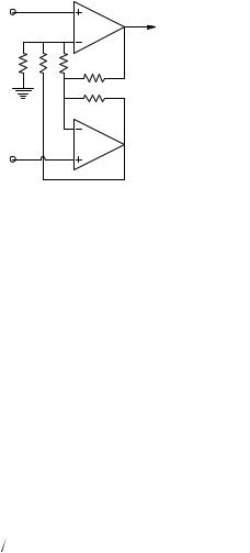
FIGURE 3.15
A two-operational amplifier DA. Resistors must be precisely matched to obtain maximum CMRR.
3.7.2Two-OP AMP DA Designs
A two-op amp DA is shown in Figure 3.15. All resistors “R” are closely matched to <0.02% to maintain a high CMRR. Analysis is easy if ideal op amps are assumed. Node equations are written for the V2 and V3 nodes, which, by the ideal op amp assumption, are Vs′ and Vs, respectively. The unknowns are Vo and V4.
Vs′ [2G + GF] − Vs GF − V4 G = 0 |
(3.38A) |
−Vs′ GF + Vs [2G + GF] − Vo G − V4 G = 0 |
(3.38B) |
Clearly, from Equation 3.38A, V4 G = Vs′[2G + GF] − Vs GF. This equation is substituted into Equation 3.38B, yielding:
o |
( s |
s ) |
( |
F ) |
|
V − V′ |
( |
F ) |
sd |
( |
F ) |
|
|
( s s ) |
|
||||||||||
V |
= V |
= V′ |
2 1 |
+ R R |
= |
|
4 1 |
+ R R |
= V |
4 1 |
+ R R |
(3.39) |
|
|
|
|
|
2 |
|
|
|
|
|
|
|
Thus, the two-op amp DA configuration can have DM gains, AD ≥ 4. (This analysis does not treat the CM gain.)
A three-op amp DA circuit is shown in Figure 3.16. In this circuit, it is assumed that all Rj = Rj′, i.e., corresponding resistors are perfectly matched in order to make the CMRR •. Analysis of the three-op amp DA can be done with superposition, but is easier if pure CM and DM excitations are assumed and the bisection theorem is used. For pure CM excitation, Vs′ = Vs = Vsc. By symmetry and the IOA assumption, V2 = V2′ = Vsc; thus, there
is no current in R1 + R1′ , and Vc = Vsc. R2 and R2′ also have no current, so no voltage drop occurs across these feedback resistors and thus V3 = V3′ = Vsc.
When the right-hand IOA circuit has matched resistors, it is a DA with gain:
V |
= (V |
3 |
− V ′ )(R |
/R |
) |
(3.40) |
o |
|
3 4 |
3 |
|
|
© 2004 by CRC Press LLC