

- •Analysis and Application of Analog Electronic Circuits to Biomedical Instrumentation
- •Dedication
- •Preface
- •Reader Background
- •Rationale
- •Description of the Chapters
- •Features
- •The Author
- •Table of Contents
- •1.1 Introduction
- •1.2 Sources of Endogenous Bioelectric Signals
- •1.3 Nerve Action Potentials
- •1.4 Muscle Action Potentials
- •1.4.1 Introduction
- •1.4.2 The Origin of EMGs
- •1.5 The Electrocardiogram
- •1.5.1 Introduction
- •1.6 Other Biopotentials
- •1.6.1 Introduction
- •1.6.2 EEGs
- •1.6.3 Other Body Surface Potentials
- •1.7 Discussion
- •1.8 Electrical Properties of Bioelectrodes
- •1.9 Exogenous Bioelectric Signals
- •1.10 Chapter Summary
- •2.1 Introduction
- •2.2.1 Introduction
- •2.2.4 Schottky Diodes
- •2.3.1 Introduction
- •2.4.1 Introduction
- •2.5.1 Introduction
- •2.5.5 Broadbanding Strategies
- •2.6 Photons, Photodiodes, Photoconductors, LEDs, and Laser Diodes
- •2.6.1 Introduction
- •2.6.2 PIN Photodiodes
- •2.6.3 Avalanche Photodiodes
- •2.6.4 Signal Conditioning Circuits for Photodiodes
- •2.6.5 Photoconductors
- •2.6.6 LEDs
- •2.6.7 Laser Diodes
- •2.7 Chapter Summary
- •Home Problems
- •3.1 Introduction
- •3.2 DA Circuit Architecture
- •3.4 CM and DM Gain of Simple DA Stages at High Frequencies
- •3.4.1 Introduction
- •3.5 Input Resistance of Simple Transistor DAs
- •3.7 How Op Amps Can Be Used To Make DAs for Medical Applications
- •3.7.1 Introduction
- •3.8 Chapter Summary
- •Home Problems
- •4.1 Introduction
- •4.3 Some Effects of Negative Voltage Feedback
- •4.3.1 Reduction of Output Resistance
- •4.3.2 Reduction of Total Harmonic Distortion
- •4.3.4 Decrease in Gain Sensitivity
- •4.4 Effects of Negative Current Feedback
- •4.5 Positive Voltage Feedback
- •4.5.1 Introduction
- •4.6 Chapter Summary
- •Home Problems
- •5.1 Introduction
- •5.2.1 Introduction
- •5.2.2 Bode Plots
- •5.5.1 Introduction
- •5.5.3 The Wien Bridge Oscillator
- •5.6 Chapter Summary
- •Home Problems
- •6.1 Ideal Op Amps
- •6.1.1 Introduction
- •6.1.2 Properties of Ideal OP Amps
- •6.1.3 Some Examples of OP Amp Circuits Analyzed Using IOAs
- •6.2 Practical Op Amps
- •6.2.1 Introduction
- •6.2.2 Functional Categories of Real Op Amps
- •6.3.1 The GBWP of an Inverting Summer
- •6.4.3 Limitations of CFOAs
- •6.5 Voltage Comparators
- •6.5.1 Introduction
- •6.5.2. Applications of Voltage Comparators
- •6.5.3 Discussion
- •6.6 Some Applications of Op Amps in Biomedicine
- •6.6.1 Introduction
- •6.6.2 Analog Integrators and Differentiators
- •6.7 Chapter Summary
- •Home Problems
- •7.1 Introduction
- •7.2 Types of Analog Active Filters
- •7.2.1 Introduction
- •7.2.3 Biquad Active Filters
- •7.2.4 Generalized Impedance Converter AFs
- •7.3 Electronically Tunable AFs
- •7.3.1 Introduction
- •7.3.3 Use of Digitally Controlled Potentiometers To Tune a Sallen and Key LPF
- •7.5 Chapter Summary
- •7.5.1 Active Filters
- •7.5.2 Choice of AF Components
- •Home Problems
- •8.1 Introduction
- •8.2 Instrumentation Amps
- •8.3 Medical Isolation Amps
- •8.3.1 Introduction
- •8.3.3 A Prototype Magnetic IsoA
- •8.4.1 Introduction
- •8.6 Chapter Summary
- •9.1 Introduction
- •9.2 Descriptors of Random Noise in Biomedical Measurement Systems
- •9.2.1 Introduction
- •9.2.2 The Probability Density Function
- •9.2.3 The Power Density Spectrum
- •9.2.4 Sources of Random Noise in Signal Conditioning Systems
- •9.2.4.1 Noise from Resistors
- •9.2.4.3 Noise in JFETs
- •9.2.4.4 Noise in BJTs
- •9.3 Propagation of Noise through LTI Filters
- •9.4.2 Spot Noise Factor and Figure
- •9.5.1 Introduction
- •9.6.1 Introduction
- •9.7 Effect of Feedback on Noise
- •9.7.1 Introduction
- •9.8.1 Introduction
- •9.8.2 Calculation of the Minimum Resolvable AC Input Voltage to a Noisy Op Amp
- •9.8.5.1 Introduction
- •9.8.5.2 Bridge Sensitivity Calculations
- •9.8.7.1 Introduction
- •9.8.7.2 Analysis of SNR Improvement by Averaging
- •9.8.7.3 Discussion
- •9.10.1 Introduction
- •9.11 Chapter Summary
- •Home Problems
- •10.1 Introduction
- •10.2 Aliasing and the Sampling Theorem
- •10.2.1 Introduction
- •10.2.2 The Sampling Theorem
- •10.3 Digital-to-Analog Converters (DACs)
- •10.3.1 Introduction
- •10.3.2 DAC Designs
- •10.3.3 Static and Dynamic Characteristics of DACs
- •10.4 Hold Circuits
- •10.5 Analog-to-Digital Converters (ADCs)
- •10.5.1 Introduction
- •10.5.2 The Tracking (Servo) ADC
- •10.5.3 The Successive Approximation ADC
- •10.5.4 Integrating Converters
- •10.5.5 Flash Converters
- •10.6 Quantization Noise
- •10.7 Chapter Summary
- •Home Problems
- •11.1 Introduction
- •11.2 Modulation of a Sinusoidal Carrier Viewed in the Frequency Domain
- •11.3 Implementation of AM
- •11.3.1 Introduction
- •11.3.2 Some Amplitude Modulation Circuits
- •11.4 Generation of Phase and Frequency Modulation
- •11.4.1 Introduction
- •11.4.3 Integral Pulse Frequency Modulation as a Means of Frequency Modulation
- •11.5 Demodulation of Modulated Sinusoidal Carriers
- •11.5.1 Introduction
- •11.5.2 Detection of AM
- •11.5.3 Detection of FM Signals
- •11.5.4 Demodulation of DSBSCM Signals
- •11.6 Modulation and Demodulation of Digital Carriers
- •11.6.1 Introduction
- •11.6.2 Delta Modulation
- •11.7 Chapter Summary
- •Home Problems
- •12.1 Introduction
- •12.2.1 Introduction
- •12.2.2 The Analog Multiplier/LPF PSR
- •12.2.3 The Switched Op Amp PSR
- •12.2.4 The Chopper PSR
- •12.2.5 The Balanced Diode Bridge PSR
- •12.3 Phase Detectors
- •12.3.1 Introduction
- •12.3.2 The Analog Multiplier Phase Detector
- •12.3.3 Digital Phase Detectors
- •12.4 Voltage and Current-Controlled Oscillators
- •12.4.1 Introduction
- •12.4.2 An Analog VCO
- •12.4.3 Switched Integrating Capacitor VCOs
- •12.4.6 Summary
- •12.5 Phase-Locked Loops
- •12.5.1 Introduction
- •12.5.2 PLL Components
- •12.5.3 PLL Applications in Biomedicine
- •12.5.4 Discussion
- •12.6 True RMS Converters
- •12.6.1 Introduction
- •12.6.2 True RMS Circuits
- •12.7 IC Thermometers
- •12.7.1 Introduction
- •12.7.2 IC Temperature Transducers
- •12.8 Instrumentation Systems
- •12.8.1 Introduction
- •12.8.5 Respiratory Acoustic Impedance Measurement System
- •12.9 Chapter Summary
- •References
410 |
Analysis and Application of Analog Electronic Circuits |
|||
|
|
+5 V |
|
|
|
|
[Vx] |
|
|
Vx |
T & H |
|
|
|
|
H |
Comp. |
|
|
|
|
|
|
|
|
|
VR |
|
|
|
|
Vo |
|
|
|
|
N-bit DAC |
|
|
|
|
N |
|
|
Start |
|
Control logic |
Status |
|
conversion |
|
and |
|
|
|
|
|
|
|
EOC |
|
output register |
CP |
Clock |
N
Digital output
FIGURE 10.12
Block diagram of the popular successive-approximation ADC.
The conversion time of an SAADC is Tc = NT, i.e., about N clock periods. For example, the Texas Instruments TLC1225 12-bit SAADC can convert in 12 μs, given a 2-MHz clock input. The TI TLC1550I 10-bit SAADC can convert in 6 μs, given a 7.8-MHz clock, which is about 166 kSa/sec.
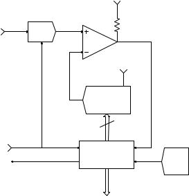
10.5.4Integrating Converters
Integrating converters are also called serial analog DACs. Two basic architectures will be considered in this section: (1) single-slope and (2) dualslope integrating DACs (IDACs). Figure 10.14 illustrates the block diagram of one version of a single-slope IDAC (SSIDAC). An op amp integrator that can be reset is used as a ramp generator; it integrates the DC VR < 0 to produce a positive ramp with slope VR/RC. The ramp, V2, is the negative input to a comparator, the positive input to which is the held signal being converted, [Vx] > 0.
At the start of conversion [Vx] > V2, so the comparator output, Q, is HI, enabling the AND gate to pass clock pulses to the binary counter. When V2 > [Vx], Q goes LO. This event stops the counting and, through the control logic, causes the integrator to be reset to V2 0 and the track and hold circuit to again track vx(t). Q 0 also causes the counter to present the total count at its parallel output and the control logic to signal end of conversion (EOC). The SSIDAC is now in standby mode waiting
© 2004 by CRC Press LLC
Digital Interfaces |
411 |
|||||||||
|
|
|
|
|
|
|
|
|
|
|
|
|
Start |
Sample & hold |
|
|
|
|
|||
|
|
Vx at t = 0 |
|
|
|
|
||||
|
|
|
|
|
|
|
|
|
||
|
|
|
|
|
|
|
|
|
|
|
|
|
|
|
|
|
|
|
|
|
|
|
|
|
|
|
Clear output |
|
|
|
|
|
|
|
|
|
|
register (all bk = 0) |
|
|
|
|
|
|
|
|
|
|
|
|
|
|
|
|
|
|
|
|
|
|
|
|
|
|
|
|
|
|
|
|
Set b1 = 1 |
|
|
|
|
|
|
|
|
|
|
(MSB HI) |
|
|
|
|
|
|
|
|
|
|
|
|
|
|
|
|
|
|
|
|
|
|
|
|
|
|
|
|
|
|
|
|
Set k = 1 in |
|
|
|
|
|
|
|
|
|
|
bit counter |
|
|
|
|
|
|
|
|
|
|
|
|
|
|
|
|
|
|
|
|
|
|
|
|
|
|
|
|
|
|
No |
|
|
|
Yes |
|||
|
|
|
|
|
|
|||||
|
|
|
|
|
Is Vx > Vo? |
|
|
|
|
|
|
|
|
|
|
|
|
||||
|
|
|
|
|
|
|
|
|
|
|
|
|
Set bk = 0 |
|
|
|
|
Leave bk = 1 |
|
||
|
|
|
|
|
|
|
|
|
|
|
|
|
|
|
|
|
|
|
|
|
|
|
|
|
|
|
|
|
|
|
|
|
(Continue) |
Increment counter |
|
|||||||
k’ = k + 1 |
|
||||||||
|
|
|
|
|
|||||
|
|
|
|
|
|
|
|
|
|
|
|
|
|
|
|
|
|
|
|
|
|
|
No |
|
|
|
Yes |
Do EOC out |
|
|
|
|
|
|
|
||||
|
|
Set bk’ = 1 |
Is k’ = 11? |
|
|
|
Latch data out |
||
|
|
|
|
|
|||||
Standby for next start
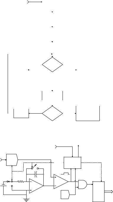
FIGURE 10.13
Logical flowchart illustrating the steps in one conversion cycle of a successive-approximation ADC.
EOC
Convert
vx(t) |
[Vx]j |
|
CON |
T & H |
|
Control |
|
|
T/H |
|
|
|
|
logic |
|
|
|
|
|
|
|
|
CP |
|
C |
|
|
|
R |
|
|
− |
|
Comp. |
Q |
|
|
|
|
VR + |
OA |
|
|
|
|
|
|
|
|
Clock |
|
CP RST
Output {bk} counter
FIGURE 10.14
Block diagram of a single-slope integrating ADC.
© 2004 by CRC Press LLC

412 |
Analysis and Application of Analog Electronic Circuits |
for the next convert (CON) command. The leading edge of the CON command causes the counter to be reset; vx(t) to be held; the integrator to begin integrating VR; and the counter to begin counting. Each completed conversion count, M, is proportional to that [Vx]. From the SSIDAC architecture, the jth conversion:
|
MjT |
|
|
|
|
|
|
RC |
|
|
[Vx ]j |
|
|||
1 |
|
|
VRdt = |
(10.36) |
|||
|
|
0 |
|||||
|
|
|
|
|
|
|
|
|
|
|
¬ |
|
|
|
|
Mj |
= |
|
[Vx ]j RC |
(10.37) |
|||
|
VRT |
|
|
||||
|
|
|
|
|
|
|
|
Suppose a 10-bit converter is desired and Vx ranges from 0 to 10 V. Let VR = 1.00 V and T = 10−6 sec. Then, from the preceding equation, it can be determined that RC = 1.023 ∞ 10−4 sec, so if C = 10−8 F, then R = 1.023 ∞ 104 Ω. With these parameters, the SSIADC will output Mj = 210 – 1 when [Vx]j = 10.0 V. Note that SSIADC conversion time is variable; the larger [Vx]j is, the longer it takes. When [Vx]j = 10 V, conversion takes 1.023 MS. Thus, integrating ADCs (IADCs) are relatively slow, suitable for ECG and DC applications. Also, accuracy of the SSIADC depends on the stability of the RC product and clock period over time and temperature changes. To overcome these problems, the clever design of the dual-slope integrating ADC was developed.
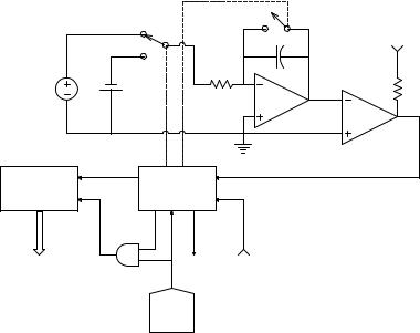
Figure 10.15 illustrates a unipolar dual-slope integrating ADC. Note it does not require a DAC. On receiving the convert command, this ADC first resets its integrator output to V2 = 0 and clears its counter to zero. S1 connects the integrator to Vx > 0. Vx is integrated for 2N clock cycles or 2N Tc sec, causing V2 to go negative. At the end of this integration time, the counter is again cleared and S1 switches to −VR, which is integrated, causing V2 to ramp positively toward zero. During this interval, the counter counts up from zero because Q is high. When V2 reaches zero, the comparator output Q goes from HI to LO, stopping the counter and signaling the end of the conversion cycle. Mathematically, the integrator output when the counter reaches T1 = 2N Tc is:
|
|
|
|
|
|
|
T1 |
|
|
|
÷ |
|
|
−2 |
N |
|
|
|
|
|
|
|
|
|
|
|
|
1 ™ |
|
|
|
™ |
|
|
|
Tc |
|
|
|
|
|
||
|
( |
|
N |
c ) |
|
|
|
|
|
|
|
{ |
|
1 } |
|
||||||
2 |
2 |
|
= − |
|
|
x |
(t) |
1 |
˝ 1 |
= |
|
|
|
x |
(10.38) |
||||||
V |
|
|
T |
RC ™ |
v |
(T )dt |
™ |
T |
RC |
V |
(T ) |
||||||||||
|
|
|
|
|
|
© 0 |
|
|
|
˛ |
|
|
|
|
|
|
|
|
|
|
|
In the second part of the conversion cycle, the integrator integrates until V2 reaches zero. This takes M clock cycles. Mathematically:
© 2004 by CRC Press LLC
Digital Interfaces |
|
|
413 |
|
|
|
|
|
S2 |
|
|
|
S1 |
+5 V |
|
|
|
V1 |
|
|
|
|
C |
|
|
|
|
|
|
|
|
−VR |
|
R |
Vx ≥ 0 |
|
|
V2 |
|
|
+ |
|
||
|
|
|
OA-2 |
|
|
|
|
|
|
|
|
|
|
Comp. |
|
RST |
|
|
Q |
N-bit |
|
Control |
|
|
|
|
|
||
counter CP |
|
logic |
|
|
|
|
EN |
CP |
|
Straight binary output |
|
EOC |
Convert |
|
Clock
FIGURE 10.15
Block diagram of a unipolar-input dual-slope integrating ADC.
|
−2N T |
|
|
|
|
|
|
|
|
MT V |
|
|||
V = 0 = |
|
|
|
(T ) + |
(10.39) |
|||||||||
|
c |
V |
c R |
|||||||||||
RC |
RC |
|||||||||||||
2 |
{ |
x |
1 |
} |
|
|
||||||||
|
|
|
|
¬ |
|
|
|
|
|
|
|
|||
|
|
|
|
|
|
|
|
|
|
|||||
|
|
V |
(T ) |
2N |
|
|
||||||||
|
M = |
{ |
x |
|
1 } |
|
|
|
|
(10.40) |
||||
|
|
|
|
|
|
|
|
|
|
|
||||
VR
Therefore, the countdown time (and thus M) is proportional to the average of the input signal over T1 = 2N Tc sec. Note that this ADC is independent of RC and Tc; these parameters are determined from practical considerations. Often T1 is made 1/60 sec to make the ADC reject 60-Hz hum on vx(t) (Northrop, 1990). Figure 10.16 illustrates the block diagram of a dual-slope integrating ADC (DSIADC).
This ADC gives an offset binary output code for bipolar DC input signals. When the convert command is given, the input is held, the counter is cleared (reset to zero), and V2 is set to zero with S2. Next, S2 is opened and S1 is set to integrate the output of OA-1, V2, for a time equal to 2N clock cycles (T1 = 2N Tc). V2 goes positive, so Q = LO, disabling the output counter. When T1 = 2N Tc, the counter is enabled and counts clock pulses, and S1 is set to integrate +VR. V2 now ramps down to zero, which is sensed by the comparator output Q going HI. The number of clock cycles required for V2 to go to 0 is M. The peak V2 is found by:
© 2004 by CRC Press LLC