

- •Analysis and Application of Analog Electronic Circuits to Biomedical Instrumentation
- •Dedication
- •Preface
- •Reader Background
- •Rationale
- •Description of the Chapters
- •Features
- •The Author
- •Table of Contents
- •1.1 Introduction
- •1.2 Sources of Endogenous Bioelectric Signals
- •1.3 Nerve Action Potentials
- •1.4 Muscle Action Potentials
- •1.4.1 Introduction
- •1.4.2 The Origin of EMGs
- •1.5 The Electrocardiogram
- •1.5.1 Introduction
- •1.6 Other Biopotentials
- •1.6.1 Introduction
- •1.6.2 EEGs
- •1.6.3 Other Body Surface Potentials
- •1.7 Discussion
- •1.8 Electrical Properties of Bioelectrodes
- •1.9 Exogenous Bioelectric Signals
- •1.10 Chapter Summary
- •2.1 Introduction
- •2.2.1 Introduction
- •2.2.4 Schottky Diodes
- •2.3.1 Introduction
- •2.4.1 Introduction
- •2.5.1 Introduction
- •2.5.5 Broadbanding Strategies
- •2.6 Photons, Photodiodes, Photoconductors, LEDs, and Laser Diodes
- •2.6.1 Introduction
- •2.6.2 PIN Photodiodes
- •2.6.3 Avalanche Photodiodes
- •2.6.4 Signal Conditioning Circuits for Photodiodes
- •2.6.5 Photoconductors
- •2.6.6 LEDs
- •2.6.7 Laser Diodes
- •2.7 Chapter Summary
- •Home Problems
- •3.1 Introduction
- •3.2 DA Circuit Architecture
- •3.4 CM and DM Gain of Simple DA Stages at High Frequencies
- •3.4.1 Introduction
- •3.5 Input Resistance of Simple Transistor DAs
- •3.7 How Op Amps Can Be Used To Make DAs for Medical Applications
- •3.7.1 Introduction
- •3.8 Chapter Summary
- •Home Problems
- •4.1 Introduction
- •4.3 Some Effects of Negative Voltage Feedback
- •4.3.1 Reduction of Output Resistance
- •4.3.2 Reduction of Total Harmonic Distortion
- •4.3.4 Decrease in Gain Sensitivity
- •4.4 Effects of Negative Current Feedback
- •4.5 Positive Voltage Feedback
- •4.5.1 Introduction
- •4.6 Chapter Summary
- •Home Problems
- •5.1 Introduction
- •5.2.1 Introduction
- •5.2.2 Bode Plots
- •5.5.1 Introduction
- •5.5.3 The Wien Bridge Oscillator
- •5.6 Chapter Summary
- •Home Problems
- •6.1 Ideal Op Amps
- •6.1.1 Introduction
- •6.1.2 Properties of Ideal OP Amps
- •6.1.3 Some Examples of OP Amp Circuits Analyzed Using IOAs
- •6.2 Practical Op Amps
- •6.2.1 Introduction
- •6.2.2 Functional Categories of Real Op Amps
- •6.3.1 The GBWP of an Inverting Summer
- •6.4.3 Limitations of CFOAs
- •6.5 Voltage Comparators
- •6.5.1 Introduction
- •6.5.2. Applications of Voltage Comparators
- •6.5.3 Discussion
- •6.6 Some Applications of Op Amps in Biomedicine
- •6.6.1 Introduction
- •6.6.2 Analog Integrators and Differentiators
- •6.7 Chapter Summary
- •Home Problems
- •7.1 Introduction
- •7.2 Types of Analog Active Filters
- •7.2.1 Introduction
- •7.2.3 Biquad Active Filters
- •7.2.4 Generalized Impedance Converter AFs
- •7.3 Electronically Tunable AFs
- •7.3.1 Introduction
- •7.3.3 Use of Digitally Controlled Potentiometers To Tune a Sallen and Key LPF
- •7.5 Chapter Summary
- •7.5.1 Active Filters
- •7.5.2 Choice of AF Components
- •Home Problems
- •8.1 Introduction
- •8.2 Instrumentation Amps
- •8.3 Medical Isolation Amps
- •8.3.1 Introduction
- •8.3.3 A Prototype Magnetic IsoA
- •8.4.1 Introduction
- •8.6 Chapter Summary
- •9.1 Introduction
- •9.2 Descriptors of Random Noise in Biomedical Measurement Systems
- •9.2.1 Introduction
- •9.2.2 The Probability Density Function
- •9.2.3 The Power Density Spectrum
- •9.2.4 Sources of Random Noise in Signal Conditioning Systems
- •9.2.4.1 Noise from Resistors
- •9.2.4.3 Noise in JFETs
- •9.2.4.4 Noise in BJTs
- •9.3 Propagation of Noise through LTI Filters
- •9.4.2 Spot Noise Factor and Figure
- •9.5.1 Introduction
- •9.6.1 Introduction
- •9.7 Effect of Feedback on Noise
- •9.7.1 Introduction
- •9.8.1 Introduction
- •9.8.2 Calculation of the Minimum Resolvable AC Input Voltage to a Noisy Op Amp
- •9.8.5.1 Introduction
- •9.8.5.2 Bridge Sensitivity Calculations
- •9.8.7.1 Introduction
- •9.8.7.2 Analysis of SNR Improvement by Averaging
- •9.8.7.3 Discussion
- •9.10.1 Introduction
- •9.11 Chapter Summary
- •Home Problems
- •10.1 Introduction
- •10.2 Aliasing and the Sampling Theorem
- •10.2.1 Introduction
- •10.2.2 The Sampling Theorem
- •10.3 Digital-to-Analog Converters (DACs)
- •10.3.1 Introduction
- •10.3.2 DAC Designs
- •10.3.3 Static and Dynamic Characteristics of DACs
- •10.4 Hold Circuits
- •10.5 Analog-to-Digital Converters (ADCs)
- •10.5.1 Introduction
- •10.5.2 The Tracking (Servo) ADC
- •10.5.3 The Successive Approximation ADC
- •10.5.4 Integrating Converters
- •10.5.5 Flash Converters
- •10.6 Quantization Noise
- •10.7 Chapter Summary
- •Home Problems
- •11.1 Introduction
- •11.2 Modulation of a Sinusoidal Carrier Viewed in the Frequency Domain
- •11.3 Implementation of AM
- •11.3.1 Introduction
- •11.3.2 Some Amplitude Modulation Circuits
- •11.4 Generation of Phase and Frequency Modulation
- •11.4.1 Introduction
- •11.4.3 Integral Pulse Frequency Modulation as a Means of Frequency Modulation
- •11.5 Demodulation of Modulated Sinusoidal Carriers
- •11.5.1 Introduction
- •11.5.2 Detection of AM
- •11.5.3 Detection of FM Signals
- •11.5.4 Demodulation of DSBSCM Signals
- •11.6 Modulation and Demodulation of Digital Carriers
- •11.6.1 Introduction
- •11.6.2 Delta Modulation
- •11.7 Chapter Summary
- •Home Problems
- •12.1 Introduction
- •12.2.1 Introduction
- •12.2.2 The Analog Multiplier/LPF PSR
- •12.2.3 The Switched Op Amp PSR
- •12.2.4 The Chopper PSR
- •12.2.5 The Balanced Diode Bridge PSR
- •12.3 Phase Detectors
- •12.3.1 Introduction
- •12.3.2 The Analog Multiplier Phase Detector
- •12.3.3 Digital Phase Detectors
- •12.4 Voltage and Current-Controlled Oscillators
- •12.4.1 Introduction
- •12.4.2 An Analog VCO
- •12.4.3 Switched Integrating Capacitor VCOs
- •12.4.6 Summary
- •12.5 Phase-Locked Loops
- •12.5.1 Introduction
- •12.5.2 PLL Components
- •12.5.3 PLL Applications in Biomedicine
- •12.5.4 Discussion
- •12.6 True RMS Converters
- •12.6.1 Introduction
- •12.6.2 True RMS Circuits
- •12.7 IC Thermometers
- •12.7.1 Introduction
- •12.7.2 IC Temperature Transducers
- •12.8 Instrumentation Systems
- •12.8.1 Introduction
- •12.8.5 Respiratory Acoustic Impedance Measurement System
- •12.9 Chapter Summary
- •References

Modulation and Demodulation of Biomedical Signals |
457 |
|
Near lock, at the output of LPF2, |
|
|
x9 [−X6vm (t)Vc 2][(ωo − ωc )t + θo − θc ] |
(11.67) |
|
so the output of mixer M3 is: |
|
|
x4 = x9 ∞ x3 = [−X6vm (t)Vc 2][vm (t)Vc X6 2][(ωo − ωc )t + θo − θc ] |
(11.68) |
|
= −[vm (t)Vc X6 2]2[(ωo − ωc )t + (θo − θc )] |
||
|
x4 tends to zero when the loop locks, leaving the VCO with phase θo = θc and ωo = ωc.
11.6 Modulation and Demodulation of Digital Carriers
11.6.1Introduction
TTL NBFM carriers can be modulated using voltage-to-frequency converter or voltage-controlled oscillator (VCO) integrated circuits. The frequency output of such an IC is given by:
fo = k1 + Kv vm(t) Hz |
(11.69) |
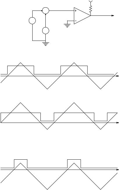
Obviously, k1 = fc, the unmodulated carrier frequency. Many VCO ICs will give simultaneous TTL, triangle, and sinusoidal wave outputs over a subhertz to +10-MHz range.
One way to produce a TTL wave whose duty cycle is modulated by vm(t) is to begin with a constant-frequency, zero-mean, symmetrical triangle wave, vT(t), as shown in Figure 11.16. vT(t) is one input to an analog comparator with TTL output; the other input is vm(t). As vm(t) approaches the peak voltage of the triangle wave, Vp, the duty cycle, η, of the TTL wave approaches unity; similarly, as vm(t) −Vp, η 0. Mathematically, the duty cycle is defined as the positive pulse width, δ, divided by the triangle wave period, T. In other words, the comparator TTL output is HI for vm(t) > vT(t).
From the foregoing, it is easy to derive the TTL wave’s duty cycle:
η = δ T = 12 [1+ vm (t) Vp ] |
(11.70) |
Here vm(t) is assumed to be changing slowly enough to be considered constant over T/2. Demodulation of a pulse width-modulated TTL carrier is
© 2004 by CRC Press LLC
458 |
Analysis and Application of Analog Electronic Circuits |
+5 V
Vo (TTL out)
+ |
COMP |
VT(t)
+
Vm(t)
Vpk
Vo
50% duty cycle
0 |
T |
VT + 0
|
VT + Vm |
Vo |
75% duty cycle |
0 |
T |
Vo
25% duty cycle
0 |
T |
VT − Vm
FIGURE 11.16
A simple pulse-width modulator and waveforms.
© 2004 by CRC Press LLC

Modulation and Demodulation of Biomedical Signals |
459 |
done by averaging the TTL pulse train and subtracting the dc component present when vm = 0.
11.6.2Delta Modulation
Now consider delta modulation (DM) and demodulation. A delta modulator is also known as a 1-bit differential pulse code modulator (DPCM). The output of a delta modulator is a clocked (periodic) train of TTL pulses with amplitudes that are HI or LO, depending on the state of the comparator output shown in Figure 11.17. The DM output basically tracks the derivative of the input signal. The comparator output is TTL HI if e(t) = [vm(t) − vr′(t)] >
0 and LO if e < 0. The D flip-flop’s (DFF) complimentary output (Q = Vo) is LO if the comparator output is HI at a positive transition of the TTL clock signal. The LO output of the DFF remains LO until the next positive transition of the clock signal; then, if the comparator output has gone LO, Vo goes high for one clock period (Tc), etc. vr′(t) is the output of the analog integrator offset by Vbias, which is one half the maximum vr ramp height over one clock
period. Vbias can be shown to be 1.1Tc/(RC) volts.
With this Vbias, when vm(t) = 0, vr′(t) will oscillate around zero with a triangle
wave with zero mean and peak height 1.1Tc/(RC) volts. Note that the Q output of the DFF must be used because the integrator gain is negative (i.e., −1/RC): a HI Vo will cause vr′ to go negative and a low Vo will make vr′ go positive. Note that vr′(t) is slew rate limited at ±(2.2 V/RC) volts/second and, if the slope of vm(t) exceeds this value, a large error will accumulate in the demodulation operation of the DM signal. (Slew rate is simply the magnitude of the first derivative of a signal, i.e., its slope.) When a DM system is tracking vm = 0, vr′(t) oscillates around zero and the DM output is a periodic square-wave 1-bit “noise.”
In adaptive delta modulation (ADM), the magnitude of the error is used to adjust the effective gain of the integrator to increase the slew rate of vr′(t) to track rapidly changing vm(t) better. One version of an ADM system is shown in Figure 11.18. Note that, ideally, the comparator should perform the signum operation; therefore, the dc value (mean) of the TTL wave must be subtracted before it is filtered, absval’d, and used to modulate the size of the square wave input to the integrator. A conventional analog multiplier is used as a modulator.
If a large error occurs as a result of poor tracking due to low slew rate in vr′(t), the comparator output will remain HI (or LO) for several clock cycles. This condition produces a nonzero signal at vf , which in turn increases the amplitude of the symmetrical pulse input to the integrator. When the ADM is tracking well, so that vr′(t) oscillates around a nearly constant vm level, then vf 0 and the peak amplitude of the error remains small. In summary, the ADM acts to minimize the mean squared error between vm(t) and vr′(t).
There are other variations on DM (e.g., sigma–delta modulation) and other types of nonlinear adaptive DM designs in addition to the one shown here.
© 2004 by CRC Press LLC

460 |
Analysis and Application of Analog Electronic Circuits |
|||||
|
|
|
CLOCK |
|
||
|
+ 5 V |
|
|
|
|
|
vm |
|
|
|
CP Q |
|
|
|
vc |
|
|
|
|
|
|
|
|
|
|
|
|
|
COMP. |
(TTL) |
D |
|
_ |
Vo |
vr’ |
|
|
|
|||
|
|
|
|
Q |
|
|
|
|
|
DFF |
(TTL) |
||
|
|
|
|
|||
|
|
|
C |
|
|
−2.4 V |
|
|
|
|
|
|
R |
|
|
vr |
|
|
|
|
|
|
|
OA |
|
|
|
−Vbias |
|
A |
(Int.) |
|
|
|
|
|
|
|
|
||
vm
 e
e
vr’
0
0
vo |
_ |
|
(DFF Q output) |
||
|
 CLOCK
CLOCK
B
FIGURE 11.17
Block diagram and waveforms of a simple delta modulator.
Much of the interest in efficient, simple, low-noise modulation schemes has been driven by the need to transmit sound and pictures over the Internet. Medical signals such as ECG and EEG also benefit from this development because of the need to transmit them from the site of the patient to a diagnostician. Biotelemetry is an important technology in the wireless monitoring of internal physiological states, sports medicine, and emergency medicine, and in ecological studies.
© 2004 by CRC Press LLC