

- •Analysis and Application of Analog Electronic Circuits to Biomedical Instrumentation
- •Dedication
- •Preface
- •Reader Background
- •Rationale
- •Description of the Chapters
- •Features
- •The Author
- •Table of Contents
- •1.1 Introduction
- •1.2 Sources of Endogenous Bioelectric Signals
- •1.3 Nerve Action Potentials
- •1.4 Muscle Action Potentials
- •1.4.1 Introduction
- •1.4.2 The Origin of EMGs
- •1.5 The Electrocardiogram
- •1.5.1 Introduction
- •1.6 Other Biopotentials
- •1.6.1 Introduction
- •1.6.2 EEGs
- •1.6.3 Other Body Surface Potentials
- •1.7 Discussion
- •1.8 Electrical Properties of Bioelectrodes
- •1.9 Exogenous Bioelectric Signals
- •1.10 Chapter Summary
- •2.1 Introduction
- •2.2.1 Introduction
- •2.2.4 Schottky Diodes
- •2.3.1 Introduction
- •2.4.1 Introduction
- •2.5.1 Introduction
- •2.5.5 Broadbanding Strategies
- •2.6 Photons, Photodiodes, Photoconductors, LEDs, and Laser Diodes
- •2.6.1 Introduction
- •2.6.2 PIN Photodiodes
- •2.6.3 Avalanche Photodiodes
- •2.6.4 Signal Conditioning Circuits for Photodiodes
- •2.6.5 Photoconductors
- •2.6.6 LEDs
- •2.6.7 Laser Diodes
- •2.7 Chapter Summary
- •Home Problems
- •3.1 Introduction
- •3.2 DA Circuit Architecture
- •3.4 CM and DM Gain of Simple DA Stages at High Frequencies
- •3.4.1 Introduction
- •3.5 Input Resistance of Simple Transistor DAs
- •3.7 How Op Amps Can Be Used To Make DAs for Medical Applications
- •3.7.1 Introduction
- •3.8 Chapter Summary
- •Home Problems
- •4.1 Introduction
- •4.3 Some Effects of Negative Voltage Feedback
- •4.3.1 Reduction of Output Resistance
- •4.3.2 Reduction of Total Harmonic Distortion
- •4.3.4 Decrease in Gain Sensitivity
- •4.4 Effects of Negative Current Feedback
- •4.5 Positive Voltage Feedback
- •4.5.1 Introduction
- •4.6 Chapter Summary
- •Home Problems
- •5.1 Introduction
- •5.2.1 Introduction
- •5.2.2 Bode Plots
- •5.5.1 Introduction
- •5.5.3 The Wien Bridge Oscillator
- •5.6 Chapter Summary
- •Home Problems
- •6.1 Ideal Op Amps
- •6.1.1 Introduction
- •6.1.2 Properties of Ideal OP Amps
- •6.1.3 Some Examples of OP Amp Circuits Analyzed Using IOAs
- •6.2 Practical Op Amps
- •6.2.1 Introduction
- •6.2.2 Functional Categories of Real Op Amps
- •6.3.1 The GBWP of an Inverting Summer
- •6.4.3 Limitations of CFOAs
- •6.5 Voltage Comparators
- •6.5.1 Introduction
- •6.5.2. Applications of Voltage Comparators
- •6.5.3 Discussion
- •6.6 Some Applications of Op Amps in Biomedicine
- •6.6.1 Introduction
- •6.6.2 Analog Integrators and Differentiators
- •6.7 Chapter Summary
- •Home Problems
- •7.1 Introduction
- •7.2 Types of Analog Active Filters
- •7.2.1 Introduction
- •7.2.3 Biquad Active Filters
- •7.2.4 Generalized Impedance Converter AFs
- •7.3 Electronically Tunable AFs
- •7.3.1 Introduction
- •7.3.3 Use of Digitally Controlled Potentiometers To Tune a Sallen and Key LPF
- •7.5 Chapter Summary
- •7.5.1 Active Filters
- •7.5.2 Choice of AF Components
- •Home Problems
- •8.1 Introduction
- •8.2 Instrumentation Amps
- •8.3 Medical Isolation Amps
- •8.3.1 Introduction
- •8.3.3 A Prototype Magnetic IsoA
- •8.4.1 Introduction
- •8.6 Chapter Summary
- •9.1 Introduction
- •9.2 Descriptors of Random Noise in Biomedical Measurement Systems
- •9.2.1 Introduction
- •9.2.2 The Probability Density Function
- •9.2.3 The Power Density Spectrum
- •9.2.4 Sources of Random Noise in Signal Conditioning Systems
- •9.2.4.1 Noise from Resistors
- •9.2.4.3 Noise in JFETs
- •9.2.4.4 Noise in BJTs
- •9.3 Propagation of Noise through LTI Filters
- •9.4.2 Spot Noise Factor and Figure
- •9.5.1 Introduction
- •9.6.1 Introduction
- •9.7 Effect of Feedback on Noise
- •9.7.1 Introduction
- •9.8.1 Introduction
- •9.8.2 Calculation of the Minimum Resolvable AC Input Voltage to a Noisy Op Amp
- •9.8.5.1 Introduction
- •9.8.5.2 Bridge Sensitivity Calculations
- •9.8.7.1 Introduction
- •9.8.7.2 Analysis of SNR Improvement by Averaging
- •9.8.7.3 Discussion
- •9.10.1 Introduction
- •9.11 Chapter Summary
- •Home Problems
- •10.1 Introduction
- •10.2 Aliasing and the Sampling Theorem
- •10.2.1 Introduction
- •10.2.2 The Sampling Theorem
- •10.3 Digital-to-Analog Converters (DACs)
- •10.3.1 Introduction
- •10.3.2 DAC Designs
- •10.3.3 Static and Dynamic Characteristics of DACs
- •10.4 Hold Circuits
- •10.5 Analog-to-Digital Converters (ADCs)
- •10.5.1 Introduction
- •10.5.2 The Tracking (Servo) ADC
- •10.5.3 The Successive Approximation ADC
- •10.5.4 Integrating Converters
- •10.5.5 Flash Converters
- •10.6 Quantization Noise
- •10.7 Chapter Summary
- •Home Problems
- •11.1 Introduction
- •11.2 Modulation of a Sinusoidal Carrier Viewed in the Frequency Domain
- •11.3 Implementation of AM
- •11.3.1 Introduction
- •11.3.2 Some Amplitude Modulation Circuits
- •11.4 Generation of Phase and Frequency Modulation
- •11.4.1 Introduction
- •11.4.3 Integral Pulse Frequency Modulation as a Means of Frequency Modulation
- •11.5 Demodulation of Modulated Sinusoidal Carriers
- •11.5.1 Introduction
- •11.5.2 Detection of AM
- •11.5.3 Detection of FM Signals
- •11.5.4 Demodulation of DSBSCM Signals
- •11.6 Modulation and Demodulation of Digital Carriers
- •11.6.1 Introduction
- •11.6.2 Delta Modulation
- •11.7 Chapter Summary
- •Home Problems
- •12.1 Introduction
- •12.2.1 Introduction
- •12.2.2 The Analog Multiplier/LPF PSR
- •12.2.3 The Switched Op Amp PSR
- •12.2.4 The Chopper PSR
- •12.2.5 The Balanced Diode Bridge PSR
- •12.3 Phase Detectors
- •12.3.1 Introduction
- •12.3.2 The Analog Multiplier Phase Detector
- •12.3.3 Digital Phase Detectors
- •12.4 Voltage and Current-Controlled Oscillators
- •12.4.1 Introduction
- •12.4.2 An Analog VCO
- •12.4.3 Switched Integrating Capacitor VCOs
- •12.4.6 Summary
- •12.5 Phase-Locked Loops
- •12.5.1 Introduction
- •12.5.2 PLL Components
- •12.5.3 PLL Applications in Biomedicine
- •12.5.4 Discussion
- •12.6 True RMS Converters
- •12.6.1 Introduction
- •12.6.2 True RMS Circuits
- •12.7 IC Thermometers
- •12.7.1 Introduction
- •12.7.2 IC Temperature Transducers
- •12.8 Instrumentation Systems
- •12.8.1 Introduction
- •12.8.5 Respiratory Acoustic Impedance Measurement System
- •12.9 Chapter Summary
- •References

6
Operational Amplifiers
6.1Ideal Op Amps
6.1.1Introduction
The operational amplifier (op amp) had its origins in the 1940 to 1960 era during which its principal use was as an active element in analog computer systems. Early op amp circuits used vacuum tubes; op amps were used as summers, subtractors, integrators, filters, etc. in analog computer systems designed to model dynamic electromechanical systems such as autopilots and motor speed controls. With the rise of digital computers in the 1960s, analog computers were largely replaced for simulations by software numerical methods such as CSMP‘, Tutsim‘, Simnon‘, Matlab®, etc. However, engineers found that the basic linear and nonlinear op amp building blocks could be used for analog signal conditioning.
With the advent of semiconductors, op amps were designed with transistors as gain elements, instead of bulky vacuum tubes. The next step, of course, was to design integrated circuit (IC) op amps, one of the first of which was the venerable (but now obsolete) LM741. (Why is the LM741 obsolete? Newer op amps with gain-bandwidth products the same as or better than that of the LM741 have lower dc bias currents (IB and IB′ ); lower dc offset voltage (Vos) and Vos tempco; lower noise; higher dc gain; higher CMRR; higher Zin; etc. and are often cheaper.)
At present, op amps are used for a wide spectrum of linear biomedical signal conditioning applications, including differential instrumentation amplifiers; electrometer amplifiers; low-drift dc signal conditioning; active filters; summers; etc. Nonlinear op amp applications have expanded to include true-RMS to dc conversion; precision rectifiers; phase-sensitive rectifiers; peak detectors; log converters; etc. Practical op amps come with a variety of specifications, including:
•dc Gain
•Common-mode rejection ratio (CMRR)
•(Open-loop) gain-bandwidth product (fT)
239
© 2004 by CRC Press LLC
240 |
Analysis and Application of Analog Electronic Circuits |
•Slew rate (η)
•Output resistance
•Input resistance; input dc bias current (IB)
•Input short-circuit dc offset voltage (VOS)
•Input current noise (ina)
•Input short-circuit voltage noise (ena).
These specifications must be included in any detailed computer simulation of an op amp-based signal conditioning circuit for analysis and/or design. However, it is often expedient for quick, pencil-and-paper analysis to use the parsimonious ideal op amp model, as described in the next section.
6.1.2Properties of Ideal OP Amps
The ideal op amp (IOA) model makes use of the following assumptions. It is a differential voltage amplifier with a single-ended output. It has infinite input impedance, gain, CMRR, and bandwidth, as well as zero output impedance, noise, IB, and VOS. The IOA output is an ideal differential voltagecontrolled voltage source. As a consequence of the infinite differential gain assumption, a general principal of closed-loop ideal op amp operation (with negative feedback) is that both input signals are equal. Put another way, (vi − vi′) = 0; therefore, a finite output is obtained when the product of zero input and infinite differential gain is considered. In mathematical terms:
(vi − vi′) Kv = (0) • = vo < • |
(6.1) |
6.1.3Some Examples of OP Amp Circuits Analyzed Using IOAs
The best way to appreciate how the ideal op amp model is used is to consider some examples. In the first example, consider the simple inverting amplifier shown in Figure 6.1(A). By the zero input voltage criterion described earlier, the inverting input must be at ground potential because the noninverting input is. This means that the inverting input (also called the op amp’s summing junction) is a virtual ground; it is forced to be at 0 V by the negative feedback through the RF – R1 voltage divider. Because the summing junction (SJ) is at 0 V, the current in R1 is, by Ohm’s law, i1 = vs/R1. i1 enters the SJ and leaves through RF. (No current flows into the IOA’s inverting input because it has infinite input resistance.) By Ohm’s law, the IOA’s output voltage must be:
vo = −i1RF = vs (−RF/R1) |
(6.2) |
Thus, the simple inverting op amp’s gain is (−RF/R1). The minus sign comes from the fact that the SJ end of RF is at 0 V and is the positive end of RF.
© 2004 by CRC Press LLC

Operational Amplifiers |
241 |
RF
R1 vi’
vo
+
vs |
vi |
A
|
R1 |
|
|
R2 |
RF |
. |
|
|
. |
Rk |
|
. |
|
|
|
|
|
|
vi’ |
vo |
vs1 |
vs2 |
vsk |
vi
B
RF |
RF |
R1 vi’ |
R1 vi’ |
vo |
vo |
vi
+
vs
C
R1 vi
++
vs’ vs |
D |
|
RF |
FIGURE 6.1
(A) An inverting op amp amplifier. (B) An inverting amplifier with multiple inputs. (C) A noninverting op amp amplifier. (D) An op amp difference amplifier.
In the second example, k voltage input signals are added in the inverting configuration; see Figure 6.1(B). Currents through each of R1, R2, R3, … Rk are added at the SJ. The net current is again found from Ohm’s law and Kirchoff’s current law:
inet = vs1/R1 + vs2/R2 +… + vsk/Rk |
(6.3) |
inet flows through RF, giving the output voltage: |
|
vo = −RF [vs1 G1 + vs2 G2 +… + vsk Gk] |
(6.4) |
where it is obvious that Gk = 1/Rk.
© 2004 by CRC Press LLC

242 |
Analysis and Application of Analog Electronic Circuits |
In the third example, consider the basic noninverting IOA circuit, shown in Figure 6.1(C). In this case, the noninverting input is forced to be vs by the source. Thus, the voltage at the SJ is also vs. Now resistors R1 and RF form a voltage divider, the input of which is some vo that will force the vi′ = vs. The voltage divider relation, Equation 6.5,
vs = vo |
|
R1 |
(6.5) |
|
R + R |
|
|||
1 |
F |
|
||
can be easily solved for vo: |
|
|
|
|
vo = vs (1 + RF/R1) |
(6.6) |
|||
If the output of the IOA is connected directly to the SJ (i.e., RF = 0), clearly, vo /vs = +1, resulting in a unity-gain buffer amplifier with infinite Rin and zero Rout.
In the next example, Figure 6.1(D) illustrates an IOA circuit configured to make a differential amplifier. Superposition is used to illustrate how this circuit works. The output from each source considered alone with the other sources set to zero is summed to give the net output. From the first example, vo′ = vs′ (−RF/R1). (vi remains zero because no current flows in the lower voltage divider with vs set to zero.) Now vs′ = 0 is set and vi due to vs is considered. From the voltage divider at the noninverting input, vi = vs
RF/(R1 + RF). Because the OA is ideal, vi′ = vi = vs RF/(R1 + RF). Using the noninverting gain relation derived in example three:
vo = [vsRF (R1 + RF )](1+ RF R1) = vs (RF R1) |
(6.7) |
Thus, the output voltage from both sources together is:
vo = [vs − vs′](RF R1) |
(6.8) |
that is, the circuit is an ideal DA with a differential gain of (RF/R1).
A simple DA circuit like this is impractical in the real world because (1) to get ideal DA performance, the actual DA must have an infinite CMRR and (2) the congruent resistors in the circuit must be perfectly matched. Also, the IOA analysis shown assumes ideal voltage sources in vs and vs′. Any finite Thevenin source resistance associated with either source will add to either R1, thus destroying the match and degrading the DA’s CMRR.
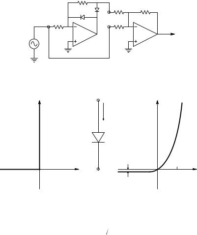
As a fifth example of the use of the IOA assumption in analyzing OA circuits, consider the full-wave rectifier circuit shown in Figure 6.2. This is a nonlinear circuit because it uses diodes. The volt–ampere behavior of a pn junction diode is often approximated by the nonlinear equation:
© 2004 by CRC Press LLC
Operational Amplifiers |
|
|
|
243 |
|
R |
|
|
|
|
|
D2 |
R/2 |
RF |
|
|
V2 |
|
|
|
|
|
|
|
R |
D1 |
|
R |
|
|
|
|
Vs |
Vo |
|
OA1 |
|
|
|
+ |
|
V3 |
OA2 |
|
|
|
|
|
Vs
FIGURE 6.2
A full-wave rectifier or absolute value circuit using two op amps.
Id |
Id |
|
|
Id > 0 |
|
|
+ |
|
|
Vd |
|
|
− |
|
Vd |
Irs |
Vd |
0 |
0 |
0.6 V |
A |
B |
|
FIGURE 6.3
(A) I–V curve of an ideal diode. (B) I–V curve of a practical diode in which iD = Irs[exp(vD/vT) − 1].
iD = IRS [exp(vD ηVT )− 1] |
(6.9) |
However, in this example the ideal diode approximation in which iD = 0 for vD < 0 and vD = 0 for iD > 0 is invoked. This relation is shown in Figure 6.3(A) and the diode equation is plotted in Figure 6.3(B). Needless to say, an ideal diode complements other electrical engineering approximations such as the ideal voltage source; current source; op amp; transformer; resistor; capacitor; and inductor.
To see how this circuit works, consider the voltages V2 and V3 as Vs is varied. First, it is obvious that if Vs = 0, V2 = V3 = 0. Now let Vs > 0. The SJ voltage remains zero and current is flows inward through the SJ. It cannot exit through D1 because current cannot flow though an ideal diode in the reverse direction. However, the current, is, does flow through RF and D1. By Ohm’s law, the voltage V2 = (Vs /R1)(−RF) = −Vs (RF/R1). V3 is infinitesimally more negative than V2 , so D2 will conduct.
© 2004 by CRC Press LLC
244 |
Analysis and Application of Analog Electronic Circuits |
Now consider Vs < 0. A current Vs /R1 leaves the SJ; D2 does not conduct. Therefore, V3 = 0 + ε. If no current flows through RF, V2 equals the SJ voltage, zero. In other words, V2 sees a Thevenin OCV = 0 through a Thevenin resistor, RF. To summarize: when Vs > 0, V2 appears as an OCV of −Vs (RF/R1) through a Thevenin series R of RF ohms. When Vs < 0, the diodes cause the OCV, V2 = 0, to appear through a Thevenin series R of RF ohms.
Vo of the output IOA is given by:
Vo = −RF [Vs G + V2 2G] |
(6.10) |
When the relations between V2 and Vs are combined in the preceding equation and R1 and RF are set equal to R, it is easy to show that, in the ideal case,
Vo = (RF/R) Vs |
(6.11) |
As a sixth example, consider the ideal op amp representation of a voltagecontrolled current source (VCCS) circuit. Figure 6.4 illustrates one version of the VCCS. The load, RL, has one end tied to ground and can be linear (a resistance) or nonlinear (e.g., a laser diode). It is clear from Ohm’s law that (Vo − VL)/RF = iL; thus, VL = Vo − iL RF. From ideal op amp behavior, the SJ voltage will be held at Vs by the feedback. Now a node equation summing the currents leaving the SJ can be written:
Vs [2G] − VL [G] − Vo [G] = 0 |
(6.12) |
The conductances cancel and VL = Vo − iLRF is substituted into the preceding equation. The final result is simply:
|
|
iL = Vs GF |
|
|
(6.13) |
|
R |
R |
|
|
|
+ |
R |
|
|
|
|
|
|
|
|
|
|
Vs |
|
(0) |
RF |
IL |
VL |
|
|
||||
|
|
POA |
|
|
|
|
|
|
Vo |
0 |
|
|
|
|
|
|
|
|
|
|
|
↓ |
RL |
|
|
(VCCS) |
|
||
|
|
|
|
||
|
|
R |
|
|
|
|
|
R |
VL |
|
|
|
−VL |
|
|
|
|
FIGURE 6.4
The three-op amp VCCS.
© 2004 by CRC Press LLC