270 |
Analysis and Application of Analog Electronic Circuits |
|
|
|
|
10 k |
|
|
HCPL-2530 |
R |
R |
V3 |
|
|
|
LED1 |
PD1 |
|
|
OA1 |
|
|
|
Ipd1 |
|
|
|
|
|
|
|
OA2 |
R |
IFB |
|
|
|
3 mA |
|
|
|
|
dc |
LED2 |
PD2 |
|
−15 V (main) |
|
|
|
|
− 5 V (iso) |
|
|
|
|
|
|
|
|
Vout |
|
3 mA dc |
|
2 k |
OA3 |
|
|
|
3.9 k
−15 V (main)
FIGURE 6.20
A linear analog photo-optic coupler used to provide galvanic isolation between the batteryoperated ECG measurement differential amplifier and band-pass filter, and the output recording and display systems.
LED2 above its 3-mA bias, increasing its light output and, in turn, increasing the photocurrent in PD2. This increases the base current in its BJT, causing the positive input of OA2 to go negative, closing a negative feedback path that compensates for LED and PD nonlinearities. Note that the ECG ground is completely isolated from the output ground, as is the analog ECG signal,
V3, from Vout. The output of the feedback POC system is taken as the voltage across the 2 k + 3.9 k resistors.
6.7Chapter Summary
This chapter has been all about op amps; it began by reviewing the properties of the ideal op amp and showing how it can be used to facilitate heuristic analysis of op amp circuits.
Practical conventional op amps were shown to be characterized by finite frequency-dependent difference-mode gains and finite input and output resistances. Their inputs were also characterized by two dc bias currents, a dc offset voltage, a short-circuit input noise voltage, and an input noise current. The various types of op amps were described, including: high frequency; high slew rate; low noise; electrometer; chopper stabilized; etc.
The effects of negative voltage feedback on a closed-loop op amp amplifier’s frequency response was described in terms of the op amp’s gain-bandwidth
Operational Amplifiers |
271 |
product, or unity gain frequency. The amplifier’s gain-bandwidth product was shown to be constant for the special case of the noninverting amplifier configuration and to be a function of the amplifier’s gain at low gains for the inverting amplifier configuration.
The current feedback amplifier (CFOA) was described and analyzed; in the noninverting gain configuration. The closed-loop amplifier’s break frequency was found to be independent of the closed-loop gain and to depend only on the absolute value of the feedback resistance. The same situation obtains for the inverting amplifier configuration using the CFOA. CFOAs were also shown to be unsuitable for integrators unless a special 2-CFOA circuit is used.
Voltage comparators were described and shown to have DA front ends and TTL or ECL logic outputs. Comparators are useful in biomedical applications, including pulse height windows used in neurophysiology and in nuclear medicine. Finally, applications of op amps as differentiators, integrators, charge amplifiers, and ECG signal conditioning were examined.
Home Problems
6.1An Apex‘ PA08A high-voltage power op amp is used to drive a resistive load. This op amp can output up to ±150 mA and swing its output voltage up to ±145 V. Its slew rate is 30 V/μs. What is the maximum Hertz frequency of a sinusoidal input it can amplify to get a 100-VRMS sinusoidal output without slew rate distortion?
6.2Figure P6.2(A) and Figure P6.2(B) illustrate a commutating auto-zero (CAZ) op amp connected as a noninverting amplifier with voltage gain (1 + RF /R1). This is an Intersil ICL7605/7606 CAZ amplifier intended for nondrifting dc amplification applications such as strain gauge bridges and electronic scales. The over-all bandwidth is made about 10 Hz. Note that the CAZ op amp has two matched op amps internally and a number of analog MOS switches to change periodically its input circuitry and switch its output. Two matched external capacitors are used to store dc offset voltages. Assume the two internal
op amps are ideal except for their offset voltages. Describe how this circuit works to realize an amazing overall offset voltage tempco of ±10 nV/∞C.
6.3Two cascaded noninverting voltage op amps are shown in Figure P6.3. Each op amp has an open-loop transfer function given by:
|
V |
105 |
|
( i |
o |
= |
|
|
i ) |
|
|
V |
− V′ |
10−3 s + 1 |
|
a.Give the Hertz gain*bandwidth product of the op amps alone.
b.Find an expression for the transfer function of the cascaded amplifiers, (V3/V1)(s), in time-constant form.
c.Give numerical values for the −3-dB frequency and the fT of the amplifier.
©2004 by CRC Press LLC
272 |
Analysis and Application of Analog Electronic Circuits |
VOS1
+
C1
|
VOS1 |
|
|
|
|
+in |
− |
+ |
|
|
|
+ |
|
|
OA-1 |
|
|
V1 |
|
|
|
A |
|
AZ |
|
|
|
Vo |
|
|
|
|
|
VOS2 |
|
|
B |
|
|
− |
+ |
|
|
Clk. |
−in |
|
|
OA-2 |
|
160 Hz |
|
|
|
|
|
|
|
R2 |
|
|
C2
R1
FIGURE P6.2A
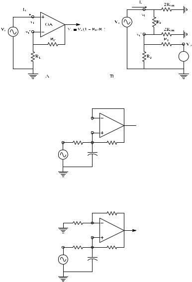
6.4Use an ECAP to simulate the response of a simple inverting op amp amplifier with a gain of −100 to a 1.0 kHz, 10 mV peak square wave. A TI TL071 op amp is used.
6.5Examine the frequency dependence of a noninverting op amp amplifier’s output impedance, Zo(jω). The circuit is shown in Figure P6.5. Let Ro = 50 Ω; RF = 99 kΩ; R1 = 1 kΩ; and Voc = (Vi − Vi′) 104/(10−3 jω +1).
a.Write an expression for Zo(jω) = It/Vt in time-constant form.
b.Make a dimensioned Bode plot of Zo(jω) (magnitude and phase).
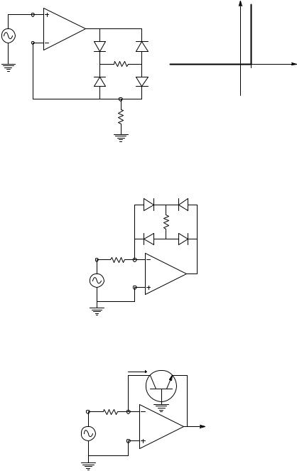
6.6A 6.2-V zener diode is used in the feedback path of an ideal op amp as shown in Figure P6.6. A simplified ZD I–V curve is shown. R1 = 1 kΩ. Plot and dimension Vo = f (V1).
274 |
Analysis and Application of Analog Electronic Circuits |
0 vi voc
Ro Vo It
vi’
R1
FIGURE P6.5
ID
−VD +
|
ID |
ZD |
(Zener I-V characteristic) |
R1 |
|
|
VD |
IOA |
−VZ |
Vo |
V1 |
0.65 V |
FIGURE P6.6
6.7A version of a diode bridge is shown in Figure P6.7. Assume v1(t) = 1.4 sin(377t) and RL = 1 kΩ. Plot and dimension several cycles of Vo(t) and V2(t). Assume the diodes have the I–V characteristic shown.
6.8Another precision rectifier bridge is shown in Figure P6.8. v1(t) and the diodes are the same as in the preceding problem. Plot and dimension several cycles of Vo(t) and V2(t).
6.9An npn BJT is used in the feedback path of an ideal op amp as shown in
Figure P6.9. The BJT is forward-biased; its collector current can be modeled
by IC Is exp(VBE /VT), where Is is the collector saturation current = 0.25 pA; VBE is the base–emitter voltage; and VT = ηkT/q 26 mV at room temperature. Plot and dimension Vo = f (V1).
276 |
|
Analysis and Application of Analog Electronic Circuits |
|
VB |
|
|
|
|
. . . |
|
|
|
|
|
|
|
|
|
|
|
|
N.O. PB |
3.3 kΩ |
R1a |
1 kΩ |
R2a |
1 kΩ |
R3a |
1 kΩ |
VR = 2.5 V |
|
|
|
|
VR |
. . . |
|
|
|
|
|
|
|
LED |
|
|
LED |
|
LED |
VR |
|
|
|
|
|
VB |
|
COM1 |
|
|
COM2 |
|
COM3 |
LM336 |
ON for |
|
ON for |
|
ON for |
VB |
> 12 V |
|
VB > 11.5 V |
|
VB > 11.0 V |
|
|
|
|
R |
|
R |
|
R |
|
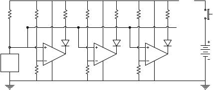
FIGURE P6.10
6.10A laptop computer uses a nominal 12-V battery. It is desired to design a bar graph type of LED voltmeter display that will measure the battery voltage over the range of 9 to 12 V. A partial schematic of the voltmeter is shown in Figure P6.10. An LM336 IC reference voltage chip supplies a constant 2.5 Vdc as long as VB > 6 V. The comparators also run off VB as long as VB > 6 V. Comparator 1 lights its LED when the voltage at its inverting terminal exceeds
VR = 2.5 V; this makes its logic output low and allows current to flow through its LED. The comparator 1 inverting terminal voltage is α1VB. α1 = R/(R + R1a). R ∫ 10 kΩ. Comparator 1’s LED lights only for VB > 12 V. Comparator 2 lights its LED for VB > 11.5 V; comparator 3’s LED lights for VB > 11.0 V; comparator 4’s LED lights for VB > 10.5 V; the comparator 5 LED lights for VB > 10.0 V; comparator 6’s LED lights for VB > 9.5 V; and comparator 7’s LED lights for VB > 9.0 V. Thus, a fully charged battery will light all seven LEDs when the button is pushed and, if 10.0 < VB < 10.5, only LEDs 5, 6, and 7 will light. Calculate the necessary values of R1a through R7a required to make the LED voltmeter work as described.
6.11Figure P6.11 shows a noninverting op amp amplifier and its equivalent input resistance circuit. Find an algebraic expression for the input admittance, Gin =
Is /Vs S. Assume that Vo = Vs (1 + RF /R1) for the amplifier. Assume that Ri and Rcm RF and R1. Evaluate Gin numerically: let Ri = 10 MΩ; Rcm = 400 MΩ; and RF = R1 = 3.3 kΩ.
6.12Find an expression for the transfer function of the filter of Figure P6.12 in time-constant form. The op amp is ideal.
6.13Find an expression for the frequency response function of the filter of Figure P6.13 in time-constant form. What function does this circuit perform on Vs?
Operational Amplifiers |
277 |
|
|
|
|
FIGURE P6.11
vi’
IOA  Vo
Vo
FIGURE P6.12
|
15 kΩ |
|
10 kΩ |
|
|
|
vi’ |
|
|
IOA |
Vo |
|
vi |
|
10 kΩ |
15 kΩ |
|
1 µF
Vs
FIGURE P6.13
6.14The circuit of Figure P6.14 is a dc millivoltmeter. Find the value of R required so that the dc microammeter reads full scale (100 μA dc) when Vs = 100 mV dc. The op amp is ideal.
6.15 Derive an expression for Vo = f (Vs, R, R) for the one active arm Wheatstone bridge signal conditioner of Figure P6.15. An ideal op amp is used.

278 |
|
Analysis and Application of Analog Electronic Circuits |
|
+ |
IOA |
Vo |
|
Vs |
|
|
|
|
|
|
Rm |
|
|
|
Im |
|
|
R |
A FS DC meter |
|
|
0 - 100 |
FIGURE P6.14
|
R + ∆R |
R |
R |
|
|
|
Vs |
|
vi’ |
|
Vo |
|
|
|
|
IOA |
R |
R |
vi |
|
|
|
|
R |
FIGURE P6.15
6.16In Figure P6.16, an ideal op amp is used control the collector current of a power BJT that supplies a relay coil. The relay coil has an inductance of 0.1 Hy and a series resistance, RL, of 30 ohms. Model the BJT by its MFSS
h-parameter model with hoe = 0. Derive expressions for the transfer functions, Vb /Vs, and Vc /Vs in time-constant form. Note that Ve /Vs = 1 because of the ideal op amp assumption. Let hfe = 19; hie = 103 Ω; and RE = 100 Ω.
a.Find an expression for Vb/Vs. Evaluate numerically.
b.Find an expression for the transfer function Vc/Vs in Laplace form. Evaluate numerically.
c.Let Vs(t) be an ideal voltage pulse that jumps to 2 V at t = 0 and to zero at t = 1 sec. Sketch and dimension Vc(t) for this input.
d.Considering the results of the preceding part of this problem, what nonlinear component can be added to the circuit to protect the transistor? Sketch the modified circuit.