


126 |
Analysis and Application of Analog Electronic Circuits |
Po
PoQ |
∆Po |
ρ ≡ ∆Po /∆ID
∆ID
ID
IDt IDQ
|
|
−Px |
|
|
|
|
|
|
|
|
|
|
V1 > 0 |
|
|
|
Px > 0 |
|
|
(DA) |
|
|
+ |
|
|
|
− |
|
|
VoQ |
Ve |
−Ki |
V3 |
Vc |
ID |
|
Po |
Vo |
|
ρ |
|
||||||||
|
|
− |
|
GM |
|
|
k |
||
+ |
|
s |
|
+ |
|
||||
|
|
|
|
|
|
||||
− |
|
(Integrator) |
(DA) |
|
(VCCS) |
(LAD Po(ID) curve) |
|
(PD amp) |
|
|
|
|
|
||||||
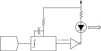
FIGURE 2.75 |
|
|
|
|
|
|
|
|
|
Top: typical LAD iD vs. vD curve, showing desired PoQ. Bottom: simplified block diagram of the regulator/modulator of Figure 2.74. See text for analysis.
Note that the final value of Po is independent of V1 and Px and is set by VoQ. Driving laser diodes safely is a complex matter; it requires a VCCS and feedback to stabilize Po against changes in temperature and supply voltage. It also requires a mechanism to protect the LAD against over-current surges at turn-on and when switching ID. Fortunately, several manufacturers now offer special ICs that stabilize Po and also permit high-frequency modulation
of the laser output intensity.
2.7Chapter Summary
This chapter introduced models for the basic semiconductor devices used in analog electronic circuits, including pn junction diodes; Schottky diodes; bipolar junction transistors (BJTs); field-effect transistors (JFETs, MOSFETs);
© 2004 by CRC Press LLC
Models for Semiconductor Devices Used in Analog Electronic Systems |
127 |
and some common solid-state photonic devices widely used in biomedical instrumentation, e.g., PIN photodiodes, avalanche photodiodes, LEDs, and laser diodes.
The circuit element models were seen to be subdivided into DC-to-mid- frequency models and high-frequency models that included small-signal capacitances resulting from charge depletion at reverse-biased pn junctions, and from stored charge in forward-conducting junctions. Mid-frequency models were used to examine the basic input resistance, voltage gain, and output resistance of simple, one-transistor BJT and FET amplifiers.
Also examined as analog IC “building blocks” were two-transistor amplifiers. High-frequency behavior of diodes, single-transistor amplifiers, and two-transistor amplifiers was examined. Certain two-transistor amplifier architectures such as the cascode and the emitter (source)-follower– grounded-base (gate) amplifier were shown to give excellent high-frequency performance because they minimized or avoided the Miller effect. Certain other broadbanding strategies were described.
Semiconductor photon sensors were introduced, including pin and avalanche photodiodes, and photoconductors. LEDs and laser diode photon sources were also covered, as well as circuits used in their operation.
Home Problems
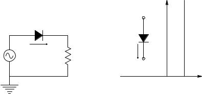
2.1A diode is used as a half-wave rectifier as shown in Figure P2.1A.
a.Assume the diode is ideal. The voltage source is vs(t) = 10 sin(377t) and the load is 10 Ω. Find the average power dissipated in the load, RL.
b.Now let the diode be represented by the I–V curve in Figure P2.1B. Find the average power dissipated in the load and also in the diode.
|
|
|
|
iD |
+ |
vD |
− |
+ |
|
|
|
|||
|
|
|
|
|
|
|
|
vD |
|
|
iD |
|
− |
|
vs |
|
|
iD |
|
|
|
|
|
vD |
|
A |
RL |
0 |
0.7 V |
|
|
B |
|
FIGURE P2.1
© 2004 by CRC Press LLC
128 |
Analysis and Application of Analog Electronic Circuits |
RL
vs
FIGURE P2.2
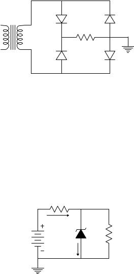
2.2A diode bridge rectifier is shown in Figure P2.2. Each diode has the I–V curve of Figure P2.1B. Find the average power in the load, RL, and also in each diode.
2.3A zener diode power supply is shown in Figure P2.3. Its purpose is to deliver 5.1 Vdc to an 85-Ω load, in which a 9-V battery is the primary dc source. A 1N751 zener diode is used; its rated voltage is 5.1 V when a 20-mA reverse (zener) current, IZ, is flowing. Find the required value for Rs. Also find the
power dissipation in the diode, Rs and RL, and the power supplied by the battery.
Rs
5.1 V
Is
9.0 V |
1N751 |
RL |
Iz
FIGURE P2.3
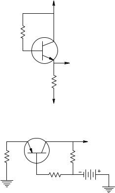
2.4Refer to the emitter follower in Figure P2.4. Given: hFE = 99, VBEQ = 0.65 V.
a.Find IBQ and RB required to make VEQ = 0 V.
b.Calculate the quiescent power dissipation in the BJT and in RE.
c.Calculate the small-signal hie for the BJT at its Q-point.
© 2004 by CRC Press LLC
Models for Semiconductor Devices Used in Analog Electronic Systems |
129 |
+12 V
RB
VEQ ≡ 0
1.2 kΩ RE
−12 V
FIGURE P2.4
VCQ
1 kΩ RE |
RC |
RB
−12 V
FIGURE P2.5
2.5A pnp BJT grounded-base amplifier is shown in Figure P2.5. Given: hFE =
149, VBEQ = 0.65 V. Find RB and RC so that the amplifier’s Q-point is at ICQ = –1.0 mA, VCEQ = −5.0 V. Find VEQ.
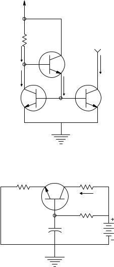
2.6The circuit shown in Figure P2.6 is a current mirror. Given: hFE = 100 (all three BJTs), VCC = +6.0 V, R = 12 kΩ, VBE1 = 0.65 = VBE2, VBE3 = 0.60 V, VCE2 VCE2sat. Find (a) VCE1; (b) IR; (c) IE3; (d) IB3; and (e) IC1 and IC2.
2.7An npn BJT grounded base amplifier is shown in Figure P2.7. Given: VBEQ = 0.65 V, hFE = 119. Find RB and RC so the Q-point is at ICQ = 2.5 mA, VCEQ = 7 V.
2.8A pnp BJT emitter follower is shown in Figure P2.8. Given: hFE = 99, VBEQ = –0.65 V.
a.Find RB and IBQ required to make VCEQ = −10 V.
b.Find the quiescent power dissipated in the BJT and in RE.
© 2004 by CRC Press LLC
130 |
Analysis and Application of Analog Electronic Circuits |
+ 6 V
12 kΩ R
IR |
|
Q3 |
IC2 |
IC1 |
|
IE3 |
|
Q1 |
Q2 |
FIGURE P2.6
RE − 7.0 V + |
RC |
1.1 kΩ |
2.5 mA |
|
RB
15 V
FIGURE P2.7
2.9Consider the three basic BJT amplifiers shown in Figure P2.9. In each amplifier, find the RB required to make ICQ = 1 mA. Also find VCEQ in each circuit. Given: hFE = 100 and VBEQ = 0.65 V.
2.10Three JFET amplifiers are shown in Figure P2.10. A “grounded-source” amplifier is shown in Figure P2.10A. The source resistor, RS, is bypassed by CS, making the source node at small-signal ground. RS is required for self-bias of the JFET. The same JFET is used in all three circuits, in which IDSS =
©2004 by CRC Press LLC

Models for Semiconductor Devices Used in Analog Electronic Systems |
131 |
− 10 V
RB
0 V
vo
1.1 kΩ
+ 5 V
FIGURE P2.8
+ 10 V
RB |
5 kΩ |
vo
100 Ω
vs
FIGURE P2.9A
6.0 mA; VP = −3.0 V; and gmo = 4 ∞ 10−3 S. In circuits (A) and (B) of Figure
P2.10, find gmQ, RS, and RD so that IDQ = 3.0 mA and VDQ = 8.0 V. Give VDSQ. Circuit (C) of Figure P2.10 is a source follower. Find R1 and RS required to
make IDQ = 3.0 mA and VSQ = 8.0 V. Neglect gate leakage current.
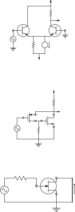
2.11The circuit of Figure P2.11 is an emitter-follower–grounded-base amplifier pair, normally used to amplify video frequency signals because it has no Miller effect. Examine its gain at mid-frequencies.
© 2004 by CRC Press LLC
132 |
Analysis and Application of Analog Electronic Circuits |
vo
100 Ω
5 kΩ
RB
vs
+ 10 V
FIGURE P2.9B
+ 10 V
RB
100 Ω
vo
vs |
5 kΩ |
|
FIGURE P2.9C
a.Draw the mid-frequency SSM for the amplifier. Let hoe = hre = 0 for both BJTs.
b.Find an expression for Avo = vo/v1. Show what happens to Avo when RE • and β1 = β2 = β.
2.12A simplified MOSFET feedback pair amplifier is shown in Figure P2.12.
a.Draw the MFSSM for the amplifier. Assume the MOSFETs have different gms (gm1, gm2) and gd1 = gd2 = 0 for simplicity.
b.Find an algebraic expression for the amplifier’s mid-frequency voltage gain, Avo = vo/v1.
c.Find an algebraic expression for the amplifier’s small-signal, Thevenin output resistance. Use the OCV/SCC method. Note
that the OCV is v1 Avo; to find the SCC, replace RL with a shortcircuit to small-signal ground and find the current in it.
© 2004 by CRC Press LLC
Models for Semiconductor Devices Used in Analog Electronic Systems |
133 |
||||
|
|
+ 15 V |
|
|
+ 15 V |
|
|
RD |
|
|
RD |
|
|
D |
RS |
S |
D |
|
|
|
|||
|
|
vo |
|
vo |
|
100 Ω |
G |
|
|
||
|
|
|
|
||
|
|
S |
vs |
G |
|
|
|
|
|
|
|
vs |
1 MΩ RG |
RS |
|
|
|
B
A
+ 15 V
IDQ
R1
D
100 Ω
G
S  vo
vo
vs 100 kΩ R2
RS
C
FIGURE P2.10
2.13See the JFET in Figure P2.13 with drain small-signal short-circuited to ground.
a.Use the high-frequency SSM for the JFET to derive an expression
for the device’s complex, short-circuit output transconductance, GM(jω) = Id/V1, at Vds ∫ 0. Assume gm, gd, Cgs, Cgd, Cds > 0 in the model.
b.Neglect the high-frequency zero at gm/Cgd r/s. Find an expression for the Hertz frequency, fT, such that rd GM(j2πfT) = 1. Express fT in terms of the quiescent drain current, IDQ. Plot fT vs. IDQ for 0 ≤
IDQ ≤ IDSS.
© 2004 by CRC Press LLC
134 |
Analysis and Application of Analog Electronic Circuits |
VCC
RL
vo
ve
v1 |
Q1 |
Q2 |
|
RE |
2 IEQ |
−VEE
FIGURE P2.11
VDD
RL
vo
G1 |
S1 |
D2 |
|
|
G2 |
|
D1 |
|
v1 |
|
S2 |
|
R1 |
|
|
|
FIGURE P2.12
R1 |
|
D |
|
|
|
|
G |
Id |
V1 |
|
|
|
S |
|
|
|
FIGURE P2.13
© 2004 by CRC Press LLC

Models for Semiconductor Devices Used in Analog Electronic Systems |
135 |
1 E3 Ω 1 E5 Ω
vo
2N2369
|
|
10 F |
15 V |
|
|
300 Ω |
|
|
|
|
|
ve |
15 V |
|
v1 |
2N2369 |
2N2369 |
||
|
||||
|
|
1.2 E3 Ω |
|
FIGURE P2.14
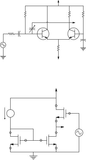
2.14An emitter-coupled cascode amplifier uses three 2N2369 BJTs as shown in Figure P2.14.
a.Use an ECAP to do a dc biasing analysis. Plot the dc Vo vs. V1. Use a 0- to15-V scale for Vo and a ±0.25-V scale for the dc input, V1. Find the amplifier’s maximum dc gain.
b. Make a |
Bode plot of |
the amplifier’s frequency response, |
|
20 log V /V |
vs. f for 105 |
≤ f ≤ 109 Hz. Give the mid-frequency |
|
o |
1 |
|
|
gain, the |
−3-dB frequency, and fT for the amplifier. |
||
c.Now put a 300-Ω resistor in series with V1. Repeat (b).
2.15An EF–GB amplifier, shown in Figure P2.15, uses capacitance
“neutralization” to effectively cancel its input capacitance and extend its highfrequency, −3-dB bandwidth. Use an ECAP to investigate how CN affects the amplifier’s high-frequency response. First, try CN = 0, then see what happens
with CN values in the tenths of a picofarad. Find CN that will give the maximum −3-dB frequency with no more than a +3-dB peak to the frequency
response Bode plot.
2.16The MOSFET source follower uses a current mirror to obtain a high equivalent RS looking into the drain of Q2. The three MOSFETs have identical MFSSMs (identical gmo, IDSS, and VP).
a.Draw the MFSSM for the circuit.
b.Find an expression for the mid-frequency gain, Avo = vo/v1.
c.Find an expression for the Thevenin output resistance presented at the vo node.
© 2004 by CRC Press LLC
136 |
Analysis and Application of Analog Electronic Circuits |
||
|
|
VCC = +12 V |
|
|
RB |
RC |
RB |
|
|
|
vo |
|
CN |
|
|
|
100 Ω |
|
|
|
1 µF |
ve |
|
|
|
|
|
|
Q1 |
Q2 |
1 µF |
V1 |
Q1 = Q2 = 2N2369 |
|
|
RE |
|
||
|
RB = 1.8 MΩ |
|
|
|
|
|
|
|
RC = 5.8 kΩ |
|
|
|
RE = 5.637 kΩ |
VEE = −12 V |
|
|
|
|
|
FIGURE P2.15 |
|
|
|
|
|
VDD |
|
|
D1 |
|
Ibias |
Q1 |
|
|
S1 |
|
|
|
vo |
D3 |
D2 |
v1 |
Q3 |
|
Q2 |
S3 |
S2 |
|
FIGURE P2.16
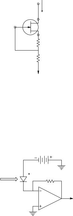
2.17A JFET circuit is used as a current sink for a differential amplifier’s “long tail.”
a.Use the high-frequency SSM for the FET to find an expression for the impedance looking into the FET’s drain, Zid(jω). (The HiFSSM includes gm, gd, Cds, Cgd, Cgs.)
b.Find the FET’s short-circuit, dc drain current, IDsc. Assume the FET’s drain current is given by ID = IDSS (1 − VGS/VP)2. Assume saturated drain operation. IDSS and VP are known.
© 2004 by CRC Press LLC
Models for Semiconductor Devices Used in Analog Electronic Systems |
137 |
id + ID
D
G
S
R1
R2
−VSS
FIGURE P2.17
2.18A Si avalanche photodiode (APD) is connected as shown in Figure P2.18. The total dark current of the APD is ID = 10 nA, its spectral responsivity at λ =
512 nm is R(λ) = 12 amps/watt at a reverse vD = −150 V. RF of the ideal op amp is 1 megohm.
a.Find Vo due to dark current alone.
b.Find the Pi at 512 nm that will give Vo = 1 V.
c.The total RMS output noise in the dark in a 1-kHz noise band-
width is 4.33 μV. Find the Pi at 512 nm that will give a DC Vo = 13 μV due to IP alone (3 ∞ the RMS noise output).
|
|
|
|
VB |
|
|
|
|
|
150 V |
|
hν |
|
|
(ID |
+ IP) |
RF |
|
|
||||
Pi |
|
|
|
|
|
|
|
|
|
|
|
|
APD |
|
|
|
|
|
|
|
|
||
|
(0) |
|
Vo |
||
|
|
|
|
|
|
IOA
FIGURE P2.18
© 2004 by CRC Press LLC
138 |
Analysis and Application of Analog Electronic Circuits |
+ 5 V
RD
LED

 2 s
2 s
TTL |
One-Shot |
VCO |
MV Q |
7406
FIGURE P2.19
2.19A single open-collector, inverting buffer gate (7406) is used to switch a GaP (green) LED on and off in a stroboscope. The ON time is 2 μsec. The flashing rate is variable from 10 flashes/sec to 104 flashes/sec. When the LED is ON, the LOW output voltage of the gate is 0.7 V, the LED’s forward current is 15 mA, and its forward drop is 2.0 V. The circuit is shown in Figure P2.19.
a.Find the required value of RD.
b.Find the electrical power input to the LED when a dc 15 mA flows.
c.Find the LED’s power input when driven by 2-μsec pulses at 104 pps.
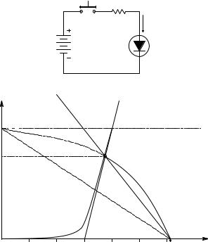
2.20A laser pointer is to be run CW from a 3.1-V (max) alkaline battery. The simple series circuit shown in Figure P2.20A is to be used to save money. Figure P2.20B shows the LAD’s iD = f(vD) curve and its linear approximation. The maximum (burnout) iD = 20 mA. The desired operating current with the 3.1-V battery is 15 mA. Three load lines are shown: (1) LL1 gives the desired operating point; (2) LL2 is always safe because the short-circuit current (SCC) can never exceed 20 mA (with LL2, the LAD cannot run at the desired 15 mA); and (3) LL3 is a nonlinear LL that allows 15-mA operation of the LAD, but limits the SCC to 20 mA.
a.Find the resistance required for LL1, RL1.
b.Find the resistance required for LL2, RL2, and the LAD’s operating point at Q2.
c.Describe how a simple tungsten lamp or a positive temperature coefficient (PTC) thermistor in series with a fixed resistor can be used to realize LL3.
© 2004 by CRC Press LLC
Models for Semiconductor Devices Used in Analog Electronic Systems |
139 |
|
|
|
|
RL |
|
|
|
A |
|
|
|
|
|
iD |
|
|
|
|
|
|
|
|
|
|
|
|
|
|
|
+ |
|
|
|
|
VB |
|
|
vD |
|
|
|
|
|
LAD |
− |
|
|
|
|
|
|
|
|
||
B |
iD (mA) |
|
|
|
|
|
|
|
|
|
LL1 |
|
|
|
|
iDmax |
20 mA |
|
|
|
|
|
|
|
|
|
|
|
|
|
|
15 mA |
|
|
|
|
|
|
|
10 mA |
|
|
|
|
|
LL3 |
|
|
|
|
|
LL2 |
|
|
P2.20B |
5 mA |
|
|
|
|
|
|
|
|
|
|
|
|
|
|
vD (V) |
0 |
|
|
|
|
|
|
|
0 |
0.5 V |
1.0 V |
1.5 V |
2.0 V |
2.5 V |
3.1 V |
|
|
|
|
|
|
|
|
|
FIGURE P2.20
© 2004 by CRC Press LLC