


Models for Semiconductor Devices Used in Analog Electronic Systems |
71 |
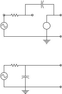
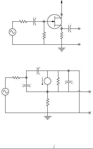
The JFET cascode amplifier’s Rin is on the order of gigaohms; its Rout is slightly lower than RD.
Two-transistor amplifiers using FETs generally have very high input resistances, gains that are not as high as equivalent two-BJT amplifiers, and more distortion in the output signal because of the nonlinear ID(VGS) characteristics of all FETs.
2.5High-Frequency Models for Transistors, and Simple Transistor Amplifiers
2.5.1Introduction
The limitation of the high-frequency bandwidth of all transistor amplifiers can be modeled by small capacitances that shunt the transistor’s small-signal model elements to ground or that connect input to output. High bandwidth is certainly not required for conditioning recorded physiological signals such as the ECG, EMG, EEG, EOG, etc. Such signals require only a low audio bandwidth for faithful reproduction. High bandwidth (into the tens of megahertz) is required for pulsed and CW ultrasound signals.
Pulse signals from sensors in imaging systems in which radioactive emissions are measured (e.g., SPECT, PET, scintimammography, etc.) also require amplifiers with bandwidths in the hundreds of megahertz or higher. Emitted ionizing radiation is detected using scintillation crystal/photomultiplier tube systems or direct semiconductor radiation sensors (Northrop, 2002).
A major goal of electronic amplifier design is to develop amplifier designs that overcome certain basic limitations on high-frequency bandwidth. A major limitation on high-frequency response is called the Miller effect. In this effect, a small-signal parasitic capacitor couples the inverting output of an ideal VCVS amplifier to its input. The circuit is shown in Figure 2.39(A); clearly, Vo = −μVg (the amplifier is inverting). Feedback to the input node is through the parasitic capacitance, Cio (normally approximately 1 to 3 pF in small-signal transistors). A node equation is written on the Vg node:
Vg [Gs + jω Cio] − Vo jω Cio = GsVs |
(2.112) |
||||||
from which |
|
|
|
|
|
||
|
V |
|
−μ |
|
|
|
|
|
o |
(jω) = |
|
|
|
|
(2.113) |
|
V |
1 |
+ jω C (1 |
+ μ)R |
|||
|
s |
|
io |
s |
|
||
is obtained.
© 2004 by CRC Press LLC
72 |
Analysis and Application of Analog Electronic Circuits |
||
|
|
Cio |
|
|
Rs |
|
|
+ |
+ |
− |
+ |
|
|
||
Vs |
Vg |
µVg Vo |
|
− |
|
+ |
− |
− |
|
||
|
|
|
|
A
|
Rs |
|
− |
|
+ |
|
|
|
µVs |
Cio (1 + µ) |
Vo |
+ |
|
|
|
− |
|
|
|
B
FIGURE 2.39
(A) Simple VCVS with negative feedback through capacitor Cio illustrating the cause of the Miller effect. (B) Simple circuit showing the Miller capacitor of the equivalent input low-pass filter. See text for analysis.
Equation 2.113 is the frequency response function of an equivalent simple R–C low-pass filter shown in Figure 2.39(B). Note that the equivalent capacitor shunting the Vg node to ground is (1 minus the voltage gain) times the parasitic feedback capacitor, Cio. This high-frequency attenuation of the input signal due to Cio is called the Miller effect.
When the ideal inverting VCVS is replaced by a Thevenin equivalent, as shown in Figure 2.40, the effect of Cio is more complex. Now it is necessary to write two node equations:
|
|
Vg [Gs + jωCio] − Vo jωCio = Vs Gs |
(2.114A) |
||||
|
|
−Vg [jωCio − μGo] + Vo [Go + jωCio] = 0 |
(2.114B) |
||||
Using Cramer’s rule to solve for Vg and Vo: |
|
|
|||||
= |
|
Gs + jωCio |
− jωCio |
|
= GsGo |
+ jωCio[Gs |
+ Go (1+ μ)] (2.115) |
|
|
||||||
|
− [jωCio − μGo ] |
[Go + jωCio ] |
|
||||
|
|
|
|
|
|
||
© 2004 by CRC Press LLC
Models for Semiconductor Devices Used in Analog Electronic Systems |
73 |
|||
|
Cio |
|
|
|
|
Rs |
Ro |
|
|
+ |
+ |
− |
+ |
|
|
|
|
|
|
Vs |
Vg |
Vg |
Vo |
|
− |
− − |
+ |
|
|
FIGURE 2.40
Another circuit illustrating the Miller effect; the effect of an output resistance is included.
|
|
Vo = Vs Gs [jωCio − μGo] |
(2.116) |
|
|
|
Vg = Vs Gs [jωCio + Go] |
(2.117) |
|
Thus: |
|
|
|
|
|
Vo |
(jω) = |
−μ[1− jωCioRo μ] |
(2.118) |
|
|
1+ jωCio[(1+ μ)Rs + Ro ] |
||
|
Vs |
|||
and: |
|
|
|
|
|
Vg |
(jω) = |
1+ jωC R |
(2.119) |
|
Vs |
1+ jωCio[(1+ μ)Rs + Ro ] |
||
|
|
|
io o |
|
From Equation 2.118, it can be seen that the break frequency of the pole still depends inversely on the Miller capacitance in the input circuit, CM = Cio(1 + μ). The Thevenin output resistance also contributes to the amplifier’s time constant. Note that the larger the gain magnitude, μ, is, the lower the break frequency. This property suggests a trade-off between gain and amplifier high-frequency bandwidth, called the gain–bandwidth product (GBWP). More will be said concerning the GBWP in following sections.
BJTs and the various types of FETs have parasitic capacitances between the input and output nodes and ground, and between the input and output nodes (the latter able to form the “evil” Miller capacitance). The following sections examine the high-frequency SSMs for BJTs and FETs, as well as the behavior of the three major single-BJT amplifiers (grounded emitter, grounded base, and emitter follower). The three major single-FET amplifiers (the grounded source, the grounded gate and source follower) will also be discussed.
© 2004 by CRC Press LLC

74 |
|
Analysis and Application of Analog Electronic Circuits |
|||||
B |
rx |
B’ |
|
Cμ |
|
C |
ic |
ib |
|
|
|
|
|
|
|
+ |
|
+ |
|
|
|
+ |
|
|
|
|
|
|
|
|
|
vbe |
|
vb’e |
rπ |
Cπ |
go |
vce |
|
|
|
− |
|
gmvb’e |
|
|
|
− |
|
|
|
− |
|
||
|
|
|
|
|
|
||
E |
|
|
|
A |
|
E |
|
|
|
|
|
|
|
|
|
B |
rx |
B’ |
|
Cμ |
|
C |
|
|
|
+ |
|
|
|
|
|
ib |
|
vb’e |
rπ |
|
go |
|
ic |
|
|
Cπ |
|
||||
|
|
− |
|
gmvb’e |
|
|
|
E |
|
|
|
|
|
E |
|
B
FIGURE 2.41
(A)The hybrid pi, high-frequency SSM for a BJT. A common-emitter configuration is assumed.
(B)A hy-pi HFSSM circuit used to calculate a BJT’s complex short-circuit output current gain, hfe (jω), and fT, where Ωhfe (j2πfT)Ω = 1.
2.5.2High-Frequency SSMs for BJTs and FETs
The simplified, hybrid-pi (hy-pi) high-frequency, small-signal model (HFSSM) is widely used to model and predict the high-frequency behavior of npn and pnp BJTs. The hy-pi model is illustrated in Figure 2.41(A). The capacitance, Cμ, is largely due to the depletion capacitance of the normally reverse-biased, collector–base junction and thus is voltage dependent. The capacitance, Cπ, is the capacitance of the forward-biased, base–emitter junction and its value can be considered to be dependent on the total emitter current. Note that the hy-pi SSM uses a Norton model for the BJT’s collector–emitter port. The output conductance, go, can be related to the BJT’s mid-frequency, h-parameter, SSM by go (hoe − gm hre) (Northrop, 1990). The VCCS has a small-signal transconductance, gm, given by:
|
= |
∂i |
|
|
|
hfe |
= |
ICQ |
(2.120) |
|
|
|
|||||||
gm |
c |
|
|
|
|
||||
∂vb′e |
|
vCe = 0 |
rπ |
VT |
|||||
|
|
|
|
|
|
The gm of BJTs is large compared with FETs and depends on the dc operating point of the device; for example, if ICQ = 1 mA, gm 0.04 S. gm is measured under small-signal, short-circuit collector–emitter conditions.
© 2004 by CRC Press LLC
Models for Semiconductor Devices Used in Analog Electronic Systems |
75 |
An important BJT parameter is its fT, the frequency at which that:
hfe |
= |
∂ic |
|
|
∂ib |
|
vce = 0 |
||
|
|
|
hfe = 1. Recall
(2.121)
When ib and ic are sine waves, hfe can be written as a complex (vector) function of frequency:
hfe (jω) = |
Ic |
(jω) |
|
(2.122) |
||||
|
||||||||
|
|
I |
b |
|
|
|
Vce |
= 0 |
Thus, by definition of fT, |
|
|
|
|||||
|
|
|
|
|
|
|||
|
hfe (j2πfT ) |
|
∫ 1 |
(2.123) |
||||
|
|
|||||||
To develop an expression for fT in terms of the hy-pi SSM parameters, consider the model shown in Figure 2.41(B). Because of the small-signal short-circuit conditions on the model, the collector current is:
Ic (jω) = gmVb′e − jωCμVb′e |
(2.124) |
Vb′e is found by writing a node equation on the B′ node:
Vb′e = |
Ib |
(2.125) |
|
gπ + jω(Cπ + Cμ ) |
|||
|
|
Substituting Equation 2.125 into Equation 2.124 yields the final result for hfe(jω):
hfe (jω) = |
Ic |
(jω) |
|
hfe (0) |
(2.126) |
||
|
= |
||||||
|
1+ jωrπ (Cπ + Cμ ) |
||||||
|
Ib |
|
Vce = 0 |
|
|||
|
|
|
|||||
hfe(0) is the lowand mid-frequency, common-emitter, h-parameter current gain, also known as the BJT’s beta. Set the magnitude of the expression of Equation 2.126 equal to unity and solve for fT:
fT = |
gm |
= |
hfe |
(0) |
= |
|
ICQ |
|
Hz |
(2.127) |
|
|
|
||||||||||
2π(Cπ + Cμ ) |
2π(Cπ + Cμ )rπ |
2π(Cπ + Cμ )VT |
|||||||||
|
|
|
|
|
|||||||
© 2004 by CRC Press LLC

76 |
|
Analysis and Application of Analog Electronic Circuits |
|
|
|
20 log hfe(jω) |
|
|
|
− 3 dB |
|
|
|
20 log[hfe(0)] |
|
|
|
−6 dB/octave |
|
|
0 dB |
ωT |
ω |
|
|
|
|
|
|
ωβ |
|
FIGURE 2.42
Bode frequency response magnitude of Ωhfe (jω)Ω.
Thus, the fT frequency for unity current gain magnitude is seen to be a function of Cπ and Cμ, as well as the BJT’s Q-point.
A Bode magnitude plot of hfe(jω) vs. ω is shown in Figure 2.42. Note that hfe(jω) has a (current) gain-bandwidth product. This is easily written from Equation 2.126:
GBWP = |
hfe (0) |
|
2πrπ (Cπ + Cμ ) Hz |
(2.128) |
Note that the hfe GBWP = fT.
It is important to note that the hy-pi HFSSM is generally valid for frequen-
cies below fT/3. To examine high-frequency BJT circuit behavior above fT/3, one must use SPICE or MicroCap‘ computer simulations, which use more
detailed, nonlinear BJT models that include effects such as carrier transit times, charge storage, how Cπ changes with VCB, etc.
A simple, linear fixed-parameter model for FET high-frequency behavior is shown in Figure 2.43. For simple modeling of FET amplifier high-fre- quency response, the three voltage-dependent capacitances, Cgs, Cgd, and Cds, are assigned values determined from the FET’s quiescent operating point. Manufacturers of discrete FETs generally do not give specific values for Cgs, Cgd, and Cds; instead they specify Ciss, the common-source short-circuit input capacitance measured with vds = 0 (small-signal drain–source voltage = 0).
From inspection of the FET HFSSM, it is obvious that Ciss = Cgd + Cgs, at some specific Q-point. Also given by manufacturers is Crss, the reverse transfer
capacitance measured with vgs = 0. From the HFSSM, it is obvious that Crss = Cds + Cgd. In general, Cgd Cds, so Crss Cgd and Cgs Ciss − Crss.
© 2004 by CRC Press LLC
Models for Semiconductor Devices Used in Analog Electronic Systems |
77 |
D
G
S
|
|
Cgd |
|
|
|
D |
|
|
|
|
|
|
+ |
G |
+ |
vgs |
|
gd |
Cds |
vds |
|
|
|||||
|
|
|
|
|
|
|
|
|
Cgs |
− |
gmvgs |
|
− |
|
|
|
|
S
FIGURE 2.43
A simple fixed-parameter HFSSM for all FETs. In JFETs, in particular, Cgd and Cgs are voltage dependent. Their values at the Q-point must be used.
G |
|
D |
|
+ |
|
+ |
|
vgs |
yis |
yos |
vds |
− |
|
yrs vds yfs vgs |
|
|
− |
|
|
S |
|
S |
|
FIGURE 2.44
The more general y-parameter HFSSM for FETs.
At VHF and UHF frequencies, the simple HFSSM of Figure 2.43 is no longer valid, so a two-port, y-parameter model is commonly used for computer modeling in which the four y-parameters are frequency dependent. The y-parameter model is illustrated in Figure 2.44. Note that this is a Norton two-port. In general, yfs(jω) = gfs + jxfs and, at midand low-frequencies, yfs =
gfs = gm; yrs 0; yis 0; and yos = gd S.
FETs are characterized by a maximum operating frequency, fmax, at which the small-signal current magnitude into the gate node, Ig(jω), equals the current magnitude, yfs Vgs , with vds = 0. From the VHFSS y-model of Figure 2.44, it is clear that fmax satisfies:
Vgs |
|
yis(j2πfmax ) |
|
= Vgs |
|
yfs(j2πfmax ) |
|
(2.129) |
|
|
|
|
© 2004 by CRC Press LLC

78 |
Analysis and Application of Analog Electronic Circuits |
It is easily seen from the fixed-parameter HFSSM of Figure 2.43 that:
fmax |
gm |
(2.130) |
|
2πCiss |
|||
|
|
Note that fmax is a device figure of merit, not a circuit figure of merit. The unity gain frequency for a grounded-source or grounded-gate FET amplifier is apt to be lower than fmax because of the Miller effect and capacitive loading, etc.
2.5.3Behavior of One-BJT and One-FET Amplifiers at High Frequencies
Figure 2.45(A) illustrates a simple, grounded-emitter (G-E) BJT amplifier. Note that the emitter is not actually grounded, but tied to ground through a parallel RE, CE. RE provides temperature stabilization of the BJT’s dc operating point; CE bypasses the emitter to ground at signal frequencies, putting the emitter at small-signal ground. Figure 2.45(B) illustrates the HFSSM of the circuit. Note that some output capacitance is generally present; it has been omitted in the model for algebraic simplicity. The base spreading resistance, rx, has also been eliminated so that two, rather than three, node equations govern the amplifier’s HF behavior. To analyze the circuit, begin by writing node equations for the Vb and Vo nodes:
Vb [Gs + gπ + jω(Cπ + Cμ)] + Vo [jωCμ] = Vs Gs |
(2.131A) |
−Vb [jωCμ − gm] + Vo [jωCμ + Gc] = 0 |
(2.131B) |
Using Cramer’s rule and a good deal of algebra, it is possible to find the midand high-frequency response function for the amplifier in time-constant form:
V |
(jω) = |
−gmRC[rπ (Rs + rπ )](1− jωCμ gm ) |
|
o |
[1− ω2CμCπRC (Rsrπ (Rs + rπ ))]+ |
(2.132) |
|
Vs |
jω[Cπ (Rsrπ (Rs + rπ ))+ CμRC + Cμ (1+ gmRC )(Rsrπ
 (Rs + rπ ))]
Note that this quadratic frequency response function has a zero at ω = gm/Cμ r/s, which is well above the BJT’s ωT, where the results predicted by the hy-pi model are no longer valid. It is therefore prudent to neglect the (1 − jωCμ/gm) term. Without this term, the frequency response function is that of a second-order low-pass filter. The Miller capacitance is Cμ (1 + gmRC); its presence provides a significant reduction of the amplifier’s high-fre- quency −3-dB point.
© 2004 by CRC Press LLC

Models for Semiconductor Devices Used in Analog Electronic Systems |
79 |
VCC
RB |
RC |
Cs |
Vo |
|
|
Rs |
|
+ |
|
Vs |
CE |
|
|
− |
RE |
|
A
Rs |
B B’ vb’e Cµ |
|
C |
+ |
|
|
+ |
Vs |
Cπ |
go |
Gc Vo |
rπ |
|||
− |
|
gmvb’e |
− |
E |
|
||
|
|
|
B
FIGURE 2.45
(A) A basic BJT “grounded-emitter” amplifier; the emitter is assumed to be at small-signal ground at midand high-frequencies. (B) Hybrid pi HFSSM for the amplifier. Note that Cμ makes a Miller feedback path between the output node and the vb′e node.
A numerical evaluation of Equation 2.132 for the grounded-emitter BJT amplifier’s frequency response is useful to appreciate its practical behavior.
Let gm = 0.01 S; rπ = 1.5 kΩ; RC = 104 Ω; Rs = 1 kΩ; Cπ = 20 pF; Cμ = 2 pF; go = 0 S; and rx = 0. The zero is found to be at ωo = gm/Cμ = 5 ∞ 109 r/s, well over
the amplifier’s ωT, which is found to be 4.55 ∞ 108 r/s. Thus, the zero is ignored.
The denominator is factored with Matlab‘ and is found to have two real poles: one at ω1 = 6.60 ∞ 106 r/s and the other at ω2 = 6.32 ∞ 108 r/s. Because ω2 is also well over ωT/3, it can be neglected. The mid-frequency gain is Avo = −60 and the Miller capacitance is CM = Cμ (1 + gmRC) = 202 pF. Finally, the G-E amplifier’s high frequency response function can thus be approximated by the one-pole LPF:
© 2004 by CRC Press LLC
80 |
Analysis and Application of Analog Electronic Circuits |
VCC
|
RC |
RB |
|
Rs |
Vo |
|
|
|
+ |
|
|
Vs |
|
|
− |
CB |
|
|
|
A
Rs ve |
|
gmve |
|
Vo |
|
|
|
|
+ |
|
Cµ |
|
Cπ |
|
rπ |
GC |
|
Vs |
|
|
− |
|
vb’e = −ve |
B,B’ |
|
|
B
FIGURE 2.46
(A) A BJT grounded-base amplifier. (B) The HFSSM for the amplifier. Note that the model does not have a Miller feedback capacitor.
Vo |
(jω) |
−60.0 |
|
|
(1+ jω 6.60 ∞ 106 ) |
(2.133) |
|
Vs |
The Hertz to 3-dB break frequency is fx = 6.60 ∞ 106/2π = 1.05 MHz, not really very high. Recall that the amplifier’s GBWP tends to remain constant; thus, to estimate fx, one can divide the BJT’s fT by its mid-frequency gain: fˆx = 7.24 ∞ 107/60 = 1.21 ∞ 106 Hz (slightly higher than fx, but in the range).
The next single-BJT amplifier circuit is the grounded-base amplifier, shown in Figure 2.46(A) and Figure 2.46(B). In the preceding treatment of the BJT G-E amplifier, feedback from the collector to the base coupled through the small-signal, collector-to-base capacitance, Cμ, gave rise to the Miller effect,
© 2004 by CRC Press LLC
Models for Semiconductor Devices Used in Analog Electronic Systems |
81 |
which caused a lowered high-frequency response. In the grounded-base (G-B) amplifier, no such feedback occurs and no Miller effect is present. Consequently, a G-B amplifier’s high-frequency response is generally better than that for a G-E amplifier, other conditions being equal.
To begin analysis of the G-B amplifier, note that the transistor’s base is bypassed to ground, causing the small-signal vb = 0. Thus, Vb′e = Vbe = Vb − Ve = Ve. Assume that rx and go = 0 for algebraic simplicity. Using the hy-pi HFSSM for the BJT, write node equations for the Ve and Vo nodes:
Ve [Gs + gπ + gm + jωCπ ] = Vs Gs |
(2.134A) |
Vo [GC + jωCμ] − Ve gm = 0 |
(2.134B) |
Because the two node equations are independent, it is simple to write:
Ve |
= |
|
|
|
|
Vs |
|
|
(2.135) |
|
+ Rs (gπ + gm ) |
+ jωCπRs |
|||||||
|
1 |
|
|||||||
|
|
|
Vo |
= |
|
Ve gmRC |
|
(2.136) |
|
|
|
|
|
+ jωCμRC |
|||||
|
|
|
|
1 |
|
||||
Substitute Equation 2.135 into Equation 2.136 and find the G-B amplifier’s frequency response function:
V |
(jω) = |
gmRC [1+ Rs (g |
π |
+ gm )] |
|
o |
|
|
|
||
|
(1+ jωCμRC ){1+ jωCπRs [1+ Rs (gπ + gm )]} |
(2.137) |
|||
Vs |
|||||
Now evaluate the frequency response function’s parameters. Let Rs =
200 Ω; rπ = 2 kΩ; gm = 0.01; RC = 104 Ω; Cμ = 2 pF; Cπ = 20 pF; rx = 0; and go = 0. From these parameters, find the noninverting, mid-frequency gain, Avo =
+32.26; ω1 = 1/(RCCμ) = 5 ∞ 107 r/s; ω2 = [1 + Rs (gπ + gm)]/RsCπ] = 7.75 ∞ 108 r/s; and ωT = 4.55 ∞ 108 r/s. Disregard ω2 because it is above ωT. Thus, the
approximate frequency response function for the G-B BJT amplifier is:
Vo |
+32.26 |
|
|
|
(jω) |
(1+ jω 5 ∞ 107 ) |
(2.138) |
Vs |
|||
The GBWP for this amplifier is 32.27 ∞ 5 ∞ 107 = 1.61 ∞ 109 r/s. Clearly, the G-B amplifier has improved high-frequency response because no Miller effect is present.
The final BJT amplifier to be considered is the emitter-follower (E-F) or grounded-collector amplifier. An E–F amplifier and its HFSSM are shown in
© 2004 by CRC Press LLC
82 |
Analysis and Application of Analog Electronic Circuits |
−VCC
RB
Rs Cs
+ |
Co |
+
Vs
RE Vo
−
−
A
Rs |
B B’ |
Cµ |
C |
+ |
rπ |
Cπ |
|
|
|
|
|
Vs |
|
gmvb’e |
|
|
|
E |
|
− |
|
|
+ |
|
|
|
|
|
|
RE |
Vo |
|
|
|
− |
|
B |
|
|
FIGURE 2.47 |
|
|
|
(A) A BJT emitter-follower. (B) The HFSSM for the amplifier. |
|
||
Figure 2.47. Node equations are written for the Vb and the Vo = Ve nodes. |
|
Assume that Rb Rs and rx = go = 0. Also, Vb′e = Vbe = (Vb − Vo). |
|
Vb[(Gs + gπ )+ s(Cμ + Cπ )]− Vo[gπ + sCπ ]= Vs Gs |
(2.139A) |
−Vb[(gπ + gm )+ sCπ ]+ Vo[(GE + gπ + gm )+ sCπ ]= 0 |
(2.139B) |
© 2004 by CRC Press LLC
Models for Semiconductor Devices Used in Analog Electronic Systems |
83 |
From Cramer’s rule: |
|
Vo = Vs Gs [(gπ + gm )+ sCπ ] |
(2.140) |
= s2Cπ Cμ + s[Cπ (Gs + GE )+ Cμ (GE + gm + gπ )]+ Gs (GE + gm + gπ )+ gπGE |
(2.141) |
The emitter follower’s frequency response function can then be written, letting s jω:
|
|
R |
( |
g |
|
+ g |
) |
1 |
+ sC |
|
( |
g |
|
+ g |
|
) |
|
Vo |
|
|
m |
|
π |
|
m |
π |
] |
|
|||||||
(s) = |
E |
|
|
|
π [ |
|
|
|
|
|
|||||||
|
s2CπCμRERs + s{Cπ (RE + Rs )+ CμRs[1+ RE (gm + gπ )]}+ |
(2.142) |
|||||||||||||||
Vs |
|||||||||||||||||
{1+ RE (gm + gπ )+ gπRs}
Note that the preceding frequency response function is not in time-constant format; to put in standard TC format, one must divide all terms by {[1 + RE (gm + gπ)] + gπ Rs}. The mid-frequency gain of the E-F amplifier is simply:
Avo |
= |
RE (1+ gmrπ ) |
|
< 1 |
(2.143) |
|
RE (1 |
+ gmrπ )+ Rs |
|
||||
|
|
+ rπ |
|
|||
Note that no Miller effect is present in an E-F amplifier, as well as no feedback from output to input; the gain is positive and <1. Let Cμ = 2 pF;
Cπ = 20 pF; gm = 0.01 S; gπ = 5 ∞ 10−4 S; Rs = 200 Ω; and RE = 104 Ω. The frequency of the zero is 5.25 ∞ 108 r/s and it can be neglected. The E-F’s poles
(break frequencies) are found to be at 2.058 ∞ 109 r/s and 4.102 ∞ 109 r/s. ωT = 4.55 ∞ 108 r/s. Because the break frequencies are 10 times the transistor’s ωT, the results are not particularly valid. What they do illustrate, however, is that the E-F has amazing bandwidth. Capacitance shunting GC (output capacitance) will lower the E-F’s high frequency response.
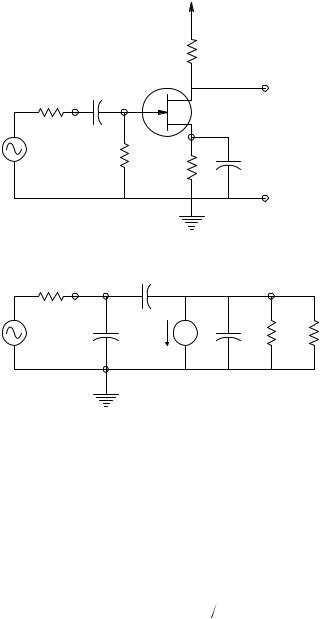
It is now appropriate to consider the high-frequency behavior of the three FET amplifiers analogous to the BJT amplifiers described previously: the FET grounded-source (G-S) amplifier; the grounded-gate (G-G) amplifier; and the source follower (S-F). Figure 2.48 illustrates a typical G-S amplifier and its HFSSM. It is clear that there will be a Miller effect for this amplifier because it has an inverting gain with magnitude >1 and a small capacitance Cgd coupling the output node to the input. The node equations for the G-S amplifier’s HFSSM are:
Vg [G1 + s(Cgs + Cgd)] − Vo[sCgd] = V1 G1 |
(2.144A) |
−Vg[−gm + sCgd] + Vo[GD′ + s(Cds + Cgd)] = 0 |
(2.144B) |
© 2004 by CRC Press LLC
84 |
Analysis and Application of Analog Electronic Circuits |
VDD
|
|
RD |
|
|
C1 |
|
|
|
R1 |
+ |
|
|
|
||
+ |
|
|
|
V1 |
|
Vo |
|
RG |
CS |
||
|
− |
RS |
|
− |
||
|
A
R1 |
Vg |
Cgd |
|
Vo |
|
|
G |
|
|
D |
|
+ |
|
|
|
|
|
V1 |
Cgs |
|
Cds |
rd |
RD |
|
|
|
|||
− |
|
gmvgs |
|
|
|
S |
|
|
|
|
|
|
|
|
|
|
B
FIGURE 2.48
(A) A JFET grounded-source amplifier. (B) The HFSSM for the amplifier.
where GD′ = GD + gd. These equations are solved with Cramer’s rule:
= G1 GD′+ s(Cds + Cgd)G1 + s(Cgs + Cgd)GD′ + s2 [(Cgs + Cgd)Cds + Cgd Cgs] (2.145)
Vo = V1 G1 [−gm + sCgd] |
(2.146) |
Thus, the detailed frequency response function for the FET G-S amplifier is:
Vo |
|
|
|
|
|
|
−g |
|
R′ |
1− sC |
|
|
g |
m ] |
|
|
|
|
|||||||
(s) = |
|
|
|
|
|
|
|
m |
|
D[ |
|
|
|
|
|
gd |
|
|
|
|
(2.147) |
||||
|
|
[ |
|
|
+ C |
|
C + C |
|
|
|
|
] |
|
|
|
+ |
|
|
|
||||||
V1 |
s2 |
|
C |
gs |
|
gd |
C |
gs |
|
R R′ |
|
|
|
|
|||||||||||
|
|
|
( |
|
gd ) ds |
|
|
|
|
|
|
1 |
D |
|
|
|
|
||||||||
|
|
s R C |
1+ g |
R′ |
|
+ R′ |
|
C |
gd |
+ C |
+ R C |
gs ] |
+ 1 |
||||||||||||
|
|
[ |
|
1 |
gd ( |
|
m D ) |
|
|
D ( |
|
|
|
|
ds ) |
1 |
|
|
|||||||
© 2004 by CRC Press LLC
Models for Semiconductor Devices Used in Analog Electronic Systems |
85 |
|||||||
|
Pick some reasonable parameters for the JFET: gd = 2 ∞ 10−5 S; IDSS = 10 mA; |
|||||||
IDQ = 5 mA; gmo = 7 ∞ 10−3 S; Cgs = Cgd = 2.5 pF; Cds = 0.5 pF; R1 = 600 Ω; and |
||||||||
R |
D |
= 3 kΩ. Thus, G′ = 3.533 ∞ 10−4 S and g |
m |
= g |
mo (IDQ ♣ IDSS) |
= 4.243 ∞ 10−3 |
S. |
|
|
D |
|
|
|
||||
|
Now the zero is at gm/Cgd = 1.70 ∞ 109 r/s, which is ridiculously high, so |
|||||||
neglect it. The mid-frequency gain is simply Avo = gmR′D |
= −12.0. To find the |
|||||||
G-S amplifier’s two break frequencies (poles), it is necessary to factor the denominator of Equation 2.147. The two break frequencies are found to be ω1 = 3.451 ∞ 107 r/s, or 5.492 ∞ 106 Hz, and ω2 = 1.950 ∞ 109 r/s. The first, lower-frequency pole is dominant and the second pole is neglected, giving the approximate frequency response for the G-S amplifier:
Vo |
(jω) |
1+ jω |
( |
−12 |
∞ 107 |
) |
(2.148) |
|
V |
3.451 |
|||||||
|
|
|||||||
1 |
|
[ |
|
|
|
|||
|
|
|
|
|
] |
|
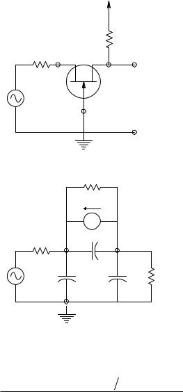
The FET analog to the BJT grounded-base circuit is the FET grounded-gate amplifier, shown in Figure 2.49(A). Assume that the dc IDQ flows through Rs and V1, self-biasing the Q point of the JFET so that VGSQ is appropriately negative. Figure 2.49(B) shows the HFSSM of the G-G amplifier. Write node
equations at Vs and Vo: |
|
|
Vs[Gs + gd + gm + s(Cgs + Cds )]− Vo[gd + sCds ]= V1Gs |
(2.149A) |
|
−Vs[gm + gd + sCds ]+ Vo GD + gd + s(Cdg |
+ Cds ) = 0 |
(2.149B) |
[ |
] |
|
Using Cramer’s rule: |
|
|
= s2[Cds (Cdg + Cgs )+ CgsCdg ] |
|
|
+ s[Gs (Cdg + Cds )+ gd (Cds + Cgs )GD (Cds + Cgs )+ gmCdg ] |
(2.150) |
|
+ [Gs (GD + gd )+ GD (gd + gm )] |
|
|
Vo = V1Gs[gm + gd + sCds ] |
|
(2.151) |
The frequency response function for the JFET G-G amplifier can finally be written after some algebra:
© 2004 by CRC Press LLC
86 |
Analysis and Application of Analog Electronic Circuits |
VDD
|
|
|
RD |
|
|
Rs |
|
|
|
|
S |
|
D |
+ |
+ |
|
|
|
|
|
|
|
|
|
V1 |
|
|
|
Vo |
− |
|
G |
|
|
|
|
|
− |
|
|
|
|
|
|
|
|
A |
|
|
|
|
gd |
|
|
|
|
gmvgs |
|
|
|
Rs Vs |
|
|
Vo |
+ |
S |
Cds |
|
D |
|
|
|
||
V1 |
|
|
|
RD |
− |
|
Cgs |
|
Cgd |
|
|
|
|
|
G
B
FIGURE 2.49
(A) A JFET grounded-gate amplifier. (B) The HFSSM for the amplifier.
Vo |
|
+R (g |
m |
+ g ) 1+ sC r |
(1+ g |
r ) |
|
|
(s) = |
D |
d [ |
ds d |
|
m d ] |
≡ (2.152) |
||
|
s2[Cds (Cdg + Cgs )+ CgsCdg ]RsRD + |
|
||||||
V1 |
|
|||||||
s[Gs (Cdg + Cds )+ (GD + gd )(Cds + Cgs )+ gmCdg ]+
[1+ gdRD + Rs (gd + gm )]
The numerical values of the the G-S amplifier: gd = 2 ∞ 10−5
FET HFSSM parameters are the same as for S; IDSS = 10 mA; IDQ = 5 mA; gmo = 7 ∞ 10−3 S;
© 2004 by CRC Press LLC

Models for Semiconductor Devices Used in Analog Electronic Systems |
87 |
Cgs = Cgd = 2.5 pF; Cds = 0.5 pF; Rs = 600 Ω; and RD = 3 kΩ; and gm = gmo (IDQ ♣ IDSS) = 4.243 ∞ 10−3 S. The G-G amplifier’s mid-band gain is:
|
|
|
|
D ( |
g |
m d |
) |
|
|
|
|
Avo |
= |
|
R |
|
r |
+ 1 |
|
= 3.535 |
(2.153) |
||
R |
g |
r |
+ |
1 + R |
|
||||||
|
|
+ r |
|
||||||||
|
|
s ( |
|
m d |
|
) |
D |
d |
|
||
The frequency of the zero is sufficiently high, so it can be neglected:
ω |
|
= ( |
g |
r + 1 |
∞ 109 r s |
(2.154) |
|
o |
|
m d |
) = 8.526 |
||||
|
|
|
Cdsrd |
|
|
|
|
|
|
|
|
|
|
|
|
Using numerical values, the quadratic denominator is factored to find the break frequencies, which are ω1 = 1.29 ∞ 108 and ω2 = 1.78 ∞ 109 r/s. Now the approximate low-pass transfer function of the G-G JFET amplifier can be written:
Vo |
(jω) |
[ |
+ jω |
3.535 |
] |
(2.155) |
V1 |
|
|||||
1 |
(1.29 ∞ 108 ) |
|||||
Note the GBWP for the G-G amplifier is 4.57 ∞ 108 r/s and the GBWP for the JFET G-S amplifier with the same parameters is found to be 4.14 ∞ 108 r/s, illustrating that gain-bandwidth product is substantially independent of amplifier gain and design for a given device.
As a final example in this one-transistor amplifier section, consider the FET source follower (S-F), shown in Figure 2.50(A). From the HFSSM, the node equations can be written:
[ |
+ s(Cgd |
] |
− Vo |
[ |
sCgs |
] |
= V1G1 |
|
Vg G1 |
+ Cgs ) |
|
|
(2.156A) |
||||
−Vg[gm + sCgs ]+ Vo[gm + Gs + gd + s(Cgs + Cds )]= 0 |
(2.156B) |
|||||||
Cramer’s rule yields:
= s2[Cgd (Cgs + Cds )+ Cgs Cds ]+ s[(Cgs + Cds )G1 + Cgd (gm + gd + GS )+ Cgs (GS + gd )]+
[G1(gm + gd + Gs )] |
(2.157) |
Vo = V1G1[gm + sCgs] |
(2.158) |
After some algebra, the frequency response function can be written:
© 2004 by CRC Press LLC
88 |
Analysis and Application of Analog Electronic Circuits |
VDD
|
|
D |
|
|
R1 |
G |
|
|
|
+ |
|
|
|
|
V1 |
|
|
+ |
|
RG |
RS |
Vo |
||
− |
||||
|
|
− |
||
|
|
|
A
|
|
Cgd |
D |
|
R1 |
Vg |
Cds |
|
G |
||
|
|
gd |
|
+ |
|
|
|
|
gmvgs |
|
|
|
|
|
|
V1 |
Cgs |
S |
+ |
|
|||
|
|
||
− |
|
RS |
Vo |
|
|
−
B
FIGURE 2.50
(A) A JFET source-follower amplifier. (B) The HFSSM for the amplifier.
V |
(s) = |
|
|
RS gm[1+ sCgs gm ] |
|
|
|
≡ (2.159) |
|||||
o |
s2[Cgd (Cgs + Cds )+ CgsCds ]R1RS + |
|
|
|
|
||||||||
V1 |
|
|
|
|
|||||||||
|
|
s R C |
+ C |
+ R C |
1 |
+ R |
(g |
m |
+ g ) |
+ R C |
[1+ g R ] |
+ |
|
|
|
{ S ( gs |
ds ) |
1 |
gd[ |
S |
|
d ] |
1 gs |
d s } |
|||
[RS (gm + gd + Gs )]
From Equation 2.159, the mid-frequency gain is:
Avo = |
|
RS |
(gm rd ) |
|
= 0.923 |
(2.160) |
||
S ( |
g |
m |
d |
) |
|
|||
|
d |
|
||||||
|
R |
|
r |
+ 1 |
+ r |
|
||
© 2004 by CRC Press LLC

Models for Semiconductor Devices Used in Analog Electronic Systems |
89 |
using the parameters of the preceding FET amplifiers. The zero is at ωo =
gm/Cgs = 1.70 ∞ 109 r/s.
The two poles found by factoring the quadratic denominator in numerical form are ω1 = 1.26 ∞ 109 and ω2 = 5.96 ∞ 108 r/s. Thus, the approximate midand high-frequency response of the JFET S-F is:
Vo |
(jω) |
|
+0.923 |
|
(2.161) |
||
1 |
[ |
( |
|
|
] |
||
|
|
|
|
||||
V |
1+ jω |
|
5.96 |
∞ 108 |
|
|
|
This section has shown how the Miller effect reduces high-frequency response in conventional grounded-emitter BJT amplifiers and groundedsource FET amplifiers. It has also shown that G-B, G-G, E-F, and S-F amplifiers do not suffer from the Miller effect and generally have their first highfrequency break frequency well above that for the same transistors used in G-E and G-S amplifiers. The following section shows that good high-frequency amplifiers essentially free of Miller effect can be made using two transistors.
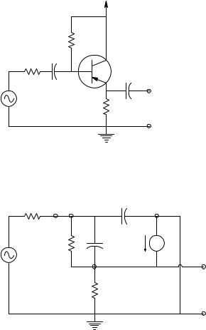
2.5.4High-Frequency Behavior of Two-Transistor Amplifiers
The loss of high-frequency amplification from the Miller effect comes from the negative feedback from output to input nodes supplied through the small drain-to-gate capacitance in FETs or through the collector-to-base capacitance in BJTs, configured as G-S and G-E amplifiers, respectively. Clearly, a good high-frequency amplifier design must avoid the Miller effect at all costs.
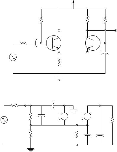
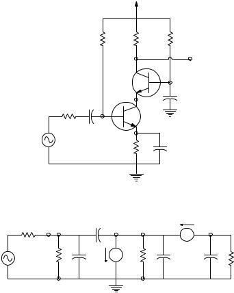
The first broadband amplifier configuration can be realized with two BJTs, two FETs, or an FET and a BJT. It is called the emitter-follower/grounded-base (EF–GB) configuration when made from BJTs. Figure 2.51 illustrates the circuit and its HFSSM. As in the previous examples of single-transistor, highfrequency amplifier analysis, write the three node equations for the HFSSM of the amplifier:
Vo[GC + sCμ2 ]− gm2Ve = 0 |
(2.162A) |
|||||
Vb[Gs + gπ1 + s(Cμ1 + Cπ1)]− Ve[gπ1 + sCπ ]= VsGs |
(2.162B) |
|||||
−Vb[gm1 + gπ1 + sCπ1]+ Ve[(gπ1 + gπ2 + gm1 + gm2 )+ GE + s(Cπ1 + Cπ2 )]= 0 |
(2.162C) |
|||||
Note that the Vo node equation is depends only on Ve; thus: |
|
|||||
|
Vo |
(s) = |
gm2RC |
|
(2.163) |
|
|
V |
1+ sC |
R |
|||
|
e |
|
μ2 |
C |
|
|
© 2004 by CRC Press LLC
90 |
Analysis and Application of Analog Electronic Circuits |
VCC
|
|
RB |
RC |
RB |
|
|
|
|
Vo |
|
Rs |
Cs |
|
|
|
Q1 |
Q2 |
|
|
+ |
|
|
Ve |
|
Vs |
|
|
|
CB2 |
− |
|
RE |
|
|
|
|
|
|
A
Rs |
B1, B1’ Vb Cμ1 |
C1 |
C2 |
Vo |
|
+ |
|
Cπ1 |
|
|
|
Vs |
|
rπ1 |
|
|
RC |
|
|
gm1vb’e1 |
gm2vb’e2 |
||
|
|
|
|
||
− |
Ve |
E1 |
|
Ve |
|
|
|
E2 |
|
||
|
|
RE |
|
Cπ2 Cμ2 |
|
|
|
|
rπ2 |
|
|
B |
B2, B2’ |
|
FIGURE 2.51
(A) A BJT emitter-follower–grounded-base amplifier. (B) The HFSSM for the amplifier.
To simplify the algebra, assume the transistors are identical and have the same ICQ. Thus,
Cπ1 = Cπ2 = Cπ , gm1 = gm2 = gm , rπ1 = rπ2 = rπ , Cμ1 = Cμ2 = Cμ ,
(2.164)
rx1 = rx2 = 0, and go1 = go2 = 0
and, using Cramer’s rule and a plethora of algebra, the frequency response for Ve can be found (let s = jω):
© 2004 by CRC Press LLC

Models for Semiconductor Devices Used in Analog Electronic Systems |
91 |
|||||||
|
Ve |
|
(1+ g |
r ) 1+ sC r |
(1+ g |
r ) |
|
|
|
(s) = |
|
m π [ |
π π |
|
m π ] |
|
|
|
|
s2 [2CπCμ + Cπ2 ]Rs rπ + |
|
|
|
(2.165) |
||
|
Vs |
|
|
|
||||
s{Cπ[2rπ + Rs (gm rπ + 2 + GE rπ )]+ Cμ Rs[2(1+ gm rπ )+ GE rπ ]}+ [2(1+ gm rπ )+ GE rπ + Rs (gm + GE )]
The mid-frequency gain of the amplifier is found by substituting Equation 2.165 into Equation 2.163 and letting s = jω = 0:
A = |
Vo |
= |
gmRC |
(2.166) |
|
2 + [rπ + Rs (1+ gmRE )] [RE (1+ gm rπ )] |
|||
vo |
Vs |
|
||
|
|
|
|
|
Note that the small-signal term, gm rπ, is equal to the BJT’s beta or hfe. Define reasonable numerical values for the EF–GB circuit’s parameters: ICQ = 1 mA;
gm = 0.0384615 S; rπ = 2.6 ∞103 Ω; Rs = 300 Ω; RC = 6 kΩ; RE = 3 kΩ; Cμ = 2 pF; and Cπ = 200 pF.
Substituting these parameters in the preceding expressions yields Avo = + 108.66. The frequency of the zero is ωo = (1 + gm rπ)/Cπ rπ = 1.942 ∞ 108 r/s. The collector break frequency is at ω3 = 1/CμRC = 8.333 ∞ 107 r/s. The other two break frequencies are found from finding the roots of the denominator of Equation 2.165; they are ω1 = 1.961 ∞ 108 and ω2 = 3.438 ∞ 107 r/s. Thus the overall frequency response function for the EF–GB amplifier is:
Vo |
|
|
|
|
[ |
|
|
] |
(2.167) |
|
(jω) = |
|
|
+108.66 1 |
+ jω (1.942 ∞ 108 ) |
||||
|
|
+ jω |
(3.438 ∞ 107 ) 1 |
+ jω |
(8.333 ∞ 107 ) 1 |
+ jω |
(1.961 ∞ 108 ) |
||
Vs |
1 |
||||||||
|
|
[ |
|
][ |
|
|
][ |
|
] |
Note that the HF pole nearly cancels the HF zero, so the final (approximate) frequency response is
Vo |
(jω) |
|
|
|
Vo + 108.66 |
|
|
|
(2.168) |
|||
|
s[ |
|
|
|
|
|
] |
|||||
s |
( |
|
|
][ |
|
( |
|
|
||||
V 1+ jω |
3.438 |
∞ 107 |
) |
1 |
+ jω |
8.333 ∞ 107 |
) |
|
||||
V |
|
|
|
|
|
|||||||
Note from the HFSSM of the EF–GB amplifier that it has no Miller capacitance coupling the output to the input and the gain is noninverting. By way of comparison, substitute the hy-pi transistor model parameters used previously into the frequency response expression for a conventional single G-E amplifier, given by Equation 2.132 in the previous section. The mid-frequency gain for this amplifier is found to be −230.8 and the dominant break frequency is at ω1 = 5.348 ∞ 106 r/s, considerably lower that that for the EF–GB amplifier.
© 2004 by CRC Press LLC
92 |
Analysis and Application of Analog Electronic Circuits |
VCC
RB RC RB
Vo
CB2
|
Cs |
|
Rs |
+ |
|
Vs |
CE |
− |
RE |
|
A
Rs B1, B1’ |
Cµ |
C1 |
E2 |
C2 Vo |
+ |
|
|
|
|
rπ Cπ |
|
|
rπ Cπ |
Cµ |
Vs |
|
|
|
GC |
−
B2, B2’
B
FIGURE 2.52
(A) A BJT cascode amplifier. (B) The HFSSM for the amplifier.
A second two-transistor amplifier that substantially avoids the Miller effect is the well-known cascode amplifier, shown in Figure 2.52(A). The two-BJT cascode amp is illustrated, but it is possible to use an FET for the lower transistor and a BJT for the top, or to use two FETs. As in the preceding
example, assume that Cπ1 = Cπ2 = Cπ, gm1 = gm2 = gm, rπ1 = rπ2 = rπ, Cμ1 = Cμ2 = Cμ, rx1 = rx2 = 0, and go1 = go2 = 0. The node equations for the HFSSM of Figure
2.52(B) are |
|
Vb [(Gs + gπ) + s(Cπ + Cμ)] − Ve [sCμ ] = Vs Gs |
(2.169A) |
− Vb [−gm + sCμ ] + Ve [(gπ + gm) + s(Cπ + Cμ)] = 0 |
(2.169B) |
Vo [GC + sCμ] − Ve gm = 0 |
(2.169C) |
© 2004 by CRC Press LLC
Models for Semiconductor Devices Used in Analog Electronic Systems
From Equation 2.169 can easily be written:
Vo |
(s) = |
gmRC |
|
V |
1+ sR C |
||
e |
|
C |
μ |
Using Cramer’s rule on Equation 2.169A and Equation 2.169B:
=s2[2CμCπ + Cπ2 ]+ s[gπ (Cπ + Cμ )+ gm (Cπ + 2Cμ )]+ [Gs (gπ + gm )+ gπ (gπ + gm )]
Ve = −Vs Gs gm [1− sCμ  gm ]
gm ]
93
(2.170)
(2.171)
(2.172)
The frequency response function for Ve can be written from the two preceding equations:
V |
(s) = |
−gm rπ [1− sCμ gm ] |
|
e |
s2[2CμCπ + Cπ2 ]+ s Rs[Cπ (1+ gmrπ )+ Cμ (1+ 2gmrπ )]+ |
(2.173) |
|
Vs |
[(1+ gmrπ )+ Rs (gπ + gm )]
From Equation 2.173 and Equation 2.169C, the cascode amplifier’s midfrequency gain, Avo, can be found:
A = |
V |
= |
−gmRC [gmrπ |
(1+ gmrπ )] |
(2.174) |
o |
|
|
|||
|
(1+ Rs |
rπ ) |
|||
vo |
Vs |
|
|
||
|
|
|
Now, using the hy-pi HFSSM parameters used in the EF–GB HF amplifier, evaluate the zero, poles, and gain, Avo, for the cascode amplifier, Avo = –204.9. The zero is at ωo = 1.923 ∞ 1010 r/s (the zero is negligible). The collector pole for the upper BJT is ω3 = 1/(RCCμ) = 8.333 ∞ 107 r/s. The two poles for the Ve frequency response function, Equation 2.173, are found to be ω1 = 1.739 ∞ 108 and ω2 = 2.036 ∞ 107 r/s. Note that ω2 is the dominant, lowest break frequency. The simplified frequency response function is thus:
Vo |
(jω) = |
|
−204.9 |
|
|
(2.175) |
|
|
[ |
( |
|
|
] |
||
s |
|
|
|
||||
V |
1+ jω |
|
2036 |
∞ 107 |
|
|
|
The high break frequency for the BJT cascode amplifier compares favorably with that for the EF–GB amplifier analyzed previously. There is no Miller
© 2004 by CRC Press LLC