

Models for Semiconductor Devices Used in Analog Electronic Systems |
105 |
||||
|
|
|
|
−iD |
R |
|
|
|
|
|
|
|
Pi |
|
|
IDL |
− Vo + |
|
|
|
|
||
|
|
|
|
Cd |
|
vD |
IP |
itn |
isn |
GL Irs |
VB |
+ |
|
|
|
|
|
iD |
|
|
|
|
|
RL >> R
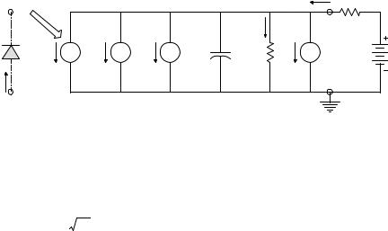
FIGURE 2.59
Model for a reverse-biased Si PIN photodiode. isn is the DC current-dependent shot noise root power spectrum; itn is the thermal noise root power spectrum. VB and R are components of the DC Thevenin circuit biasing the PD.
D* is 1/NEP for the detector element only, normalized to a 1 cm2 active area. D* is used only for comparisons between PDs of different active areas. D* units are cm Hz/W. (A “better” PD has a higher D*.)
2.6.3Avalanche Photodiodes
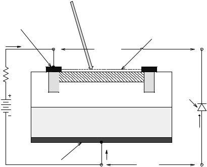
A cross-sectional schematic of an avalanche PD (APD) is shown in Figure 2.60. In an APD, a large reverse-biasing voltage is used, about 100 V or more, depending on diode design. The internal E-field completely depletes the π-region of mobile carriers. The E-field in the π-region causes any injected or thermally generated carriers to attain a saturation velocity, giving them enough kinetic energy so that their impact with valence-band electrons causes ionization — the creation of other electron–hole pairs — that in turn are accelerated by the E-field, causing still more impact ionizations, etc.
Photon-generated electron–hole pairs are separated by the E-field in the p- and π-regions; electrons move into the n+ layer and holes drift into the p+ layer, both of which are boundaries of the APD’s space-charge region. These photon-generated carriers are multiplied as they pass through the avalanche region by the impact ionization process. At a given reverse operating voltage, −vDQ = VR, one electron generated by photon collision produces M electrons at the APD’s anode. The contribution of electrons to IP is much greater than that from holes because electrons generated in the p- and π-regions are pulled into the avalanche region, whereas holes are swept back into the p+ region (including the holes generated in the avalanche process).
APD noise is due to shot noise. As in the case of the PIN PD, the shot noise is a broadband (white) Gaussian noise whose mean-squared value is proportional to the net DC component of the APD’s anode current, IDtot. The DC anode current has two components; dark leakage current, IL, and DC photocurrent, IP. The mean-squared shot noise current is given by:
i 2 |
= 2 qB I |
Dtot |
msV |
(2.195) |
n |
|
|
|
© 2004 by CRC Press LLC
106 Analysis and Application of Analog Electronic Circuits
|
hν |
|
Pi |
Cathode metal |
|
ring |
AR coating |
IP |
Cathode |
|
R |
n+ |
|
n |
||
n |
||
|
p |
|
|
Equivalent |
|
π region |
diode |
VB |
|
|
|
p+ |
iD |
|
|
Backside metallization
iD
Anode
FIGURE 2.60
Cross-sectional layer cake model of an avalanche photodiode.
It is clear that the lowest APD shot noise occurs when the ADP is operated at very low (average) light levels. Figure 2.61 illustrates the peak gain and RMS shot noise current as a function of the DC reverse-bias voltage on a “typical” Si APD. The total leakage current, IL, can be written as:
IL = ILS + M ILB |
(2.196) |
where ILS is the surface leakage current (not amplified) and ILB is the bulk leakage current (amplified by the avalanche process). The theoretical MS shot noise current may also be written (Perkin-Elmer, 2003):
|
= 2qB I |
|
+ I |
|
M2 + PR |
(λ)M F |
} |
|
|
i 2 |
LS |
LB |
msA |
(2.197) |
|||||
n |
{ |
[ |
i 1 |
] |
|
|
where q is the electron charge magnitude; ILS is the dark surface leakage current; ILB is the dark bulk leakage current; IP = Pi R1(λ) M is the amplified DC photocurrent; and F is the excess noise factor. In general, F = ρM + (1 − ρ) (2 − 1/M). Because M ♠ 100, F 2 + ρM. The parameter, ρ, is the ratio of hole to-electron ionization probabilities and is <1. M is the voltage-depen- dent APD internal gain. It is defined as the ratio of the output current at a given Pi, λ, and DC reverse-bias voltage, VR, to the output current for the
© 2004 by CRC Press LLC

Models for Semiconductor Devices Used in Analog Electronic Systems |
107 |
Gain (M) or Noise Current (pA/√Hz)
103
200
100
20
M
10
2.0
1.0
in
0.2
0.1
0 |
20 |
40 |
60 |
80 |
100 |
120 |
140 |
160 |
180 |
200 |
Reverse Bias Voltage, V.
FIGURE 2.61
Plot of peak photonic gain, M, and shot noise root power spectrum, in, for a typical avalanche PD.
same input (Pi and λ), but at a low dc reverse-bias voltage, say 10 V. Pi is the incident optical power at wavelength λ, R(λ,VD) is the spectral responsivity in A/W, and B is the Hertz noise bandwidth.
The PE C30902S APD has the following parameters at a reverse voltage of approximately 225 V: F = 0.02M + 0.98(2 − 1/M). M = 250 at 830 nm; thus, F = 6.956. The responsivity at 830 nm is R(λ) = 128 A/W. (Dividing the responsivity at 830 nm by M yields R1(830) = 0.512 A/W.) Total dark current is ID = 1 ∞ 10−8 A. The noise current root spectrum is in = 1.1 ∞ 10−13 RMSA/ Hz. The shunt capacitance is Cd = 1.6 pF. The rise time and fall time to an 830-nm light pulse with a 50 Ω RL (10 to 90%) is tr = tf = 0.5 ns.
The wavelength range of the APD responsivity curve, R(λ), depends on APD material; Si APDs are useful between 300 to 1100 nm, Ge APDs between 800 and 1600 nm, and InGaAs devices between 900 to 1700 nm. The peak responsivity depends on the average reverse-bias voltage on the APD. R1(λ) is defined as the APD’s responsivity at a low VR such that M = 1. Thus, the APD’s (amplified) photocurrent can be written
IP = Pi R1(λ) M = Pi R(λ) amps |
(2.198) |
© 2004 by CRC Press LLC
108 |
Analysis and Application of Analog Electronic Circuits |
|
|
|
rms shot |
|
rmsA |
signal current, |
noise current |
||
|
rmsA |
_________________ |
||
|
|
|||
|
|
|
√2qB(Pi R1(λ)MF + IL) |
|
|
IP = Pi R1(λ)M |
|
|
|
|
|
|
max SNR |
|
|
|
|
thermal noise |
_______ |
|
|
|
current |
√4kTGLB |
1 |
10 |
Mopt |
100 |
103 |
|
|
|
Gain M |
|
FIGURE 2.62
Plot of signal current and RMS shot noise current for a typical APD vs. gain M, showing the optimum M where the diode’s RMS SNR is maximum.
at a given λ and VR, as shown in Equation 2.195. As noted earlier, the total shot noise from an APD depends not only on dc leakage current, but also on dc photocurrent. There is also a noise current from any Thevenin conductance shunting the APD. Thus, the total diode noise in MSA is given by:
|
= 2qB{ILS + [ILBM2 + Pi R1(λ)M]F}+ 4k T GL B msA |
|
in2 |
(2.199) |
The APD’s MSSNR can be written, noting that F 2 + ρM:
SNR = |
|
|
|
|
|
P |
2R 2 (λ)M2 |
|
|
|
|
|
|
|
||||
|
|
|
|
|
|
i |
|
1 |
|
|
|
|
|
|
|
|
|
|
2qB I |
LS |
+ I |
LB |
M |
+ PR (λ) MF |
} |
+ 4k T G B |
|
|
|||||||||
|
{ |
[ |
|
|
|
i |
1 |
] |
|
L |
(2.200) |
|||||||
|
|
|
|
|
|
|
|
|
|
P 2R 2 (λ) |
B |
|
||||||
= |
|
|
|
|
|
|
|
|
|
|
|
|
|
|||||
|
|
|
|
|
|
|
|
|
i |
1 |
|
|
|
|
|
|
|
|
|
2q I |
LS |
M2 + |
I |
LB |
+ PR |
(λ) M |
] |
(2 |
+ ρM) |
+ 4k T G M2 |
|
||||||
|
{ |
|
[ |
|
i 1 |
|
|
|
} |
|
L |
|||||||
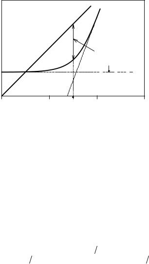
Inspection of the denominator of the right-hand SNR expression shows that it has a minimum at some M = Mo, which results in a maximum SNR, other factors remaining constant. This optimum Mo is illustrated in Figure 2.62. Recall that M is set by the DC reverse bias on the APD, VR, so finding the optimum VR and M to optimize the APD SNR can be arty.
2.6.4Signal Conditioning Circuits for Photodiodes
The most basic signal conditioning circuit for a PD is the simple DC Thevenin circuit shown in Figure 2.57. As discussed in the text, the output voltage
© 2004 by CRC Press LLC
Models for Semiconductor Devices Used in Analog Electronic Systems |
109 |
|
|
VB |
+ |
|
|
Pi |
|
PD |
|
RF |
iD |
|
|
|
|||
|
|
|
|
|
|
hν |
IP |
|
|
|
|
|
|
(0) |
|
Vo |
|
|
|
|
|
IOA |
|
|
Pi |
= 0 |
|
|
|
|
(dark) |
−VB |
|
|
|
|
|
|
|
vD |
|
|
|
|
|
|
|
|
|
|
|
IP = qη(Pi λ /hc) |
|
|
Increasing light |
|
|
|
|
|
intensity |
|
|
|
|
|
|
|
|
Load-line |
|
|
|
|
|
|
−VB /R |
FIGURE 2.63
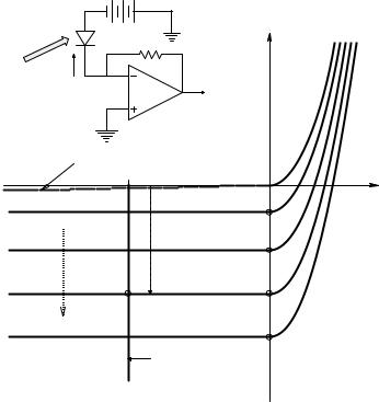
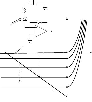
Top: op amp signal conditioning circuit for a PIN PD operated at constant bias voltage. Bottom: plot of PD iD vs. vD curves showing the constant voltage load line.
from the photocurrent can be found graphically using the load line determined by VB and R. Neglecting dark current, it is simply:
Vo = qη(Pi λ/hc)R volts |
(2.201) |
An active circuit commonly used to condition PD output is shown in Figure 2.63. Because the summing junction of the op amp is at virtual ground, the PD is held at a constant reverse bias, VB. IP flows through RF, so Ohm’s law tells that Vo = qη(Pi λ/hc) RF, neglecting leakage (dark) current. By operating a PIN PD at reverse bias, the junction depletion capacitance, Cd, is made smaller and the diode’s bandwidth is increased. Unfortunately, reverse bias also increases the leakage current and thus the device’s shot noise. If VB is made zero, then Cd is maximum and the PD’s bandwidth is lowest. At zero bias, the leakage current 0 and the diode’s shot noise is minimal, depending only on the photocurrent. As Chapter 9 will show, RF and the op amp contribute noise to Vo; this noise will not be discussed here, however.
© 2004 by CRC Press LLC
110 |
Analysis and Application of Analog Electronic Circuits |
|
VB |
+ |
|
|
|
|
|
IP |
R |
|
|
Pi |
PD |
RF |
iD |
|
|||
hν |
|
|
|
|
(0) |
IOA |
Vo |
|
|
|
|
IP = qη(Pi λ /hc) |
|
|
|
Pi |
= 0 |
|
|
(dark) |
|
|
|
−VB |
|
|
vD |
|
|
|
|
Increasing light |
|
|
|
intensity |
|
|
|
|
|
Load-line |
|
|
|
|
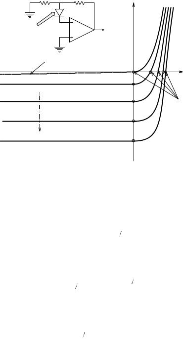
−VB /R |
FIGURE 2.64
Top: op amp signal conditioning circuit for a PIN PD biased from a Thevenin dc source. Bottom: plot of PD iD vs. vD curves showing the load line.
Sometimes a resistor is added in series with VB to limit the current through the PD. This circuit is shown in Figure 2.64. Note that the maximum PD current is determined by the load line and is iD = −VB/R. APDs are run with the same circuit, except VB is on the order of hundreds of volts and the series R (typically ≥1 MΩ) serves to protect the APD from excess reverse current that, for most APDs, is on the order of hundreds of microamperes. Although the series resistor protects the ADP from excess reverse current, it also produces thermal (Johnson) noise over and above the APD’s shot noise, as well as the noise produced in the op amp circuit
An op amp circuit can be used to condition the output of a PIN PD to yield a logarithmic output proportional to Pi, as shown in Figure 2.65. The PD is operated in the zero current mode. Solving for vDoc:
© 2004 by CRC Press LLC
Models for Semiconductor Devices Used in Analog Electronic Systems |
111 |
|
R1 |
vDoc |
RF |
|
|
iD |
|
|
|
PD |
|
|
|
|
|
Pi |
hν |
(0) |
Vo |
|
|
IOA |
|
|
|
|
|
|
Pi |
= 0 |
|
|
(dark) |
|
|
|
|
|
vD |
|
|
|
vDoc |
Increasing light |
|
||
intensity |
|
|
|
FIGURE 2.65
Top: op amp signal conditioning circuit for a PIN PD operated in the open-circuit photovoltage
mode. Bottom: plot of PD iD vs. vD curves showing the operating points.
iD = 0 = Irs[exp(vDoc  VT )− 1]− qη(Pi λ
 hc)
hc)
|
|
¬ |
|
|
|
|
|
|
|
|
|
|
qη P λ |
hc |
) |
˘ |
|
v |
= V |
ln 1 |
+ |
( |
i |
|
˙ |
|
|
|
|
|
|||||
Doc |
T |
|
|
|
Irs |
|
|
|
|
|
|
|
|
|
|
˙ |
|
|
|
|
|
|
|
|
|
˚ |
and, because of the R1, RF voltage divider, this yields:
|
|
|
|
qη Pλ hc |
˘ |
||
Vo = (1+ RF |
R1)VT |
ln 1 |
+ |
( |
i |
) |
˙ |
|
Irs |
|
|||||
|
|
|
|
|
|
˙ |
|
|
|
|
|
|
|
|
˚ |
(2.202A)
(2.202B)
(2.203)
At very low light powers, using the relation ln (1 + ε) ε, Vo can be approximated by:
|
qη |
P |
λ hc ˆ |
|
|||
Vo (1+ RF |
R1)VT |
( |
i |
|
) |
˜ |
(2.204) |
|
Irs |
|
|||||
|
|
|
|
↓ |
|
||
© 2004 by CRC Press LLC
112 |
|
Analysis and Application of Analog Electronic Circuits |
||||
|
|
2 |
BB OPT202 |
|
||
|
|
|
|
|||
|
|
|
1MΩ |
RF |
|
4 |
|
|
|
3 pF |
|
|
|
|
|
IP |
|
|
|
|
|
Pi |
|
|
|
175Ω |
Vo |
|
hν |
|
PD |
|
|
5 |
|
|
|
|
|
|
|
|
|
8 |
|
1 |
3 |
|
|
|
|
|
V+ |
V− |
|
Spectral Responsivity
0.5
w/ internal V/µW Ω
1 M RF
0.4
0.3 |
|
|
|
|
0.2 |
|
|
|
|
0.1 |
|
|
|
|
0 |
|
|
|
|
200 |
400 |
600 |
800 |
1000 |
λ (nm)
FIGURE 2.66
Top: schematic of the Burr–Brown OPT202 IC photosensor. Bottom: spectral sensitivity of the OPT202 sensor. See text for details.
Typical parameter values are (1 + RF/R1) = 103, VT = kT/q = 0.0258, q = 1.602 ∞ 10−19 Cb, η 0.8, λ = 512 nm, h = 6.625 ∞ 10−34 J.sec, c = 3 ∞ 108 m/s, Irs 1 nA, and NEP 5 ∞ 10−14 W. Neglecting leakage (dark) current, Vo can be calculated for Pi = 1 pW at λ = 512 nm: Vo = 8.51 mV.
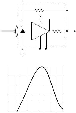
Several manufacturers make ICs containing a PIN photodiode with an onchip amplifier e.g., Burr–Brown makes the OPT202. This photosensor has a 2.29 ∞ 2.29 mm PD coupled to an op amp with an internal 1-MΩ feedback
resistor, as shown in Figure 2.66. This IC works over a wide supply voltage range (±2.25 to ±18 V) and has a voltage output responsivity of 0.45 V/μW
at λ = 650 nm with its internal RF = 1 MΩ. It has a −3-dB bandwidth of 50 kHz and a 10 to 90% rise time of 10 μs. To alter system responsivity, the RF can
be made larger or smaller than the internal 1 MΩ RF. The IC’s NEP is 10–11 W for B = 1 kHz and λ = 650 nm with RF = 1 MΩ.
© 2004 by CRC Press LLC