

- •Analysis and Application of Analog Electronic Circuits to Biomedical Instrumentation
- •Dedication
- •Preface
- •Reader Background
- •Rationale
- •Description of the Chapters
- •Features
- •The Author
- •Table of Contents
- •1.1 Introduction
- •1.2 Sources of Endogenous Bioelectric Signals
- •1.3 Nerve Action Potentials
- •1.4 Muscle Action Potentials
- •1.4.1 Introduction
- •1.4.2 The Origin of EMGs
- •1.5 The Electrocardiogram
- •1.5.1 Introduction
- •1.6 Other Biopotentials
- •1.6.1 Introduction
- •1.6.2 EEGs
- •1.6.3 Other Body Surface Potentials
- •1.7 Discussion
- •1.8 Electrical Properties of Bioelectrodes
- •1.9 Exogenous Bioelectric Signals
- •1.10 Chapter Summary
- •2.1 Introduction
- •2.2.1 Introduction
- •2.2.4 Schottky Diodes
- •2.3.1 Introduction
- •2.4.1 Introduction
- •2.5.1 Introduction
- •2.5.5 Broadbanding Strategies
- •2.6 Photons, Photodiodes, Photoconductors, LEDs, and Laser Diodes
- •2.6.1 Introduction
- •2.6.2 PIN Photodiodes
- •2.6.3 Avalanche Photodiodes
- •2.6.4 Signal Conditioning Circuits for Photodiodes
- •2.6.5 Photoconductors
- •2.6.6 LEDs
- •2.6.7 Laser Diodes
- •2.7 Chapter Summary
- •Home Problems
- •3.1 Introduction
- •3.2 DA Circuit Architecture
- •3.4 CM and DM Gain of Simple DA Stages at High Frequencies
- •3.4.1 Introduction
- •3.5 Input Resistance of Simple Transistor DAs
- •3.7 How Op Amps Can Be Used To Make DAs for Medical Applications
- •3.7.1 Introduction
- •3.8 Chapter Summary
- •Home Problems
- •4.1 Introduction
- •4.3 Some Effects of Negative Voltage Feedback
- •4.3.1 Reduction of Output Resistance
- •4.3.2 Reduction of Total Harmonic Distortion
- •4.3.4 Decrease in Gain Sensitivity
- •4.4 Effects of Negative Current Feedback
- •4.5 Positive Voltage Feedback
- •4.5.1 Introduction
- •4.6 Chapter Summary
- •Home Problems
- •5.1 Introduction
- •5.2.1 Introduction
- •5.2.2 Bode Plots
- •5.5.1 Introduction
- •5.5.3 The Wien Bridge Oscillator
- •5.6 Chapter Summary
- •Home Problems
- •6.1 Ideal Op Amps
- •6.1.1 Introduction
- •6.1.2 Properties of Ideal OP Amps
- •6.1.3 Some Examples of OP Amp Circuits Analyzed Using IOAs
- •6.2 Practical Op Amps
- •6.2.1 Introduction
- •6.2.2 Functional Categories of Real Op Amps
- •6.3.1 The GBWP of an Inverting Summer
- •6.4.3 Limitations of CFOAs
- •6.5 Voltage Comparators
- •6.5.1 Introduction
- •6.5.2. Applications of Voltage Comparators
- •6.5.3 Discussion
- •6.6 Some Applications of Op Amps in Biomedicine
- •6.6.1 Introduction
- •6.6.2 Analog Integrators and Differentiators
- •6.7 Chapter Summary
- •Home Problems
- •7.1 Introduction
- •7.2 Types of Analog Active Filters
- •7.2.1 Introduction
- •7.2.3 Biquad Active Filters
- •7.2.4 Generalized Impedance Converter AFs
- •7.3 Electronically Tunable AFs
- •7.3.1 Introduction
- •7.3.3 Use of Digitally Controlled Potentiometers To Tune a Sallen and Key LPF
- •7.5 Chapter Summary
- •7.5.1 Active Filters
- •7.5.2 Choice of AF Components
- •Home Problems
- •8.1 Introduction
- •8.2 Instrumentation Amps
- •8.3 Medical Isolation Amps
- •8.3.1 Introduction
- •8.3.3 A Prototype Magnetic IsoA
- •8.4.1 Introduction
- •8.6 Chapter Summary
- •9.1 Introduction
- •9.2 Descriptors of Random Noise in Biomedical Measurement Systems
- •9.2.1 Introduction
- •9.2.2 The Probability Density Function
- •9.2.3 The Power Density Spectrum
- •9.2.4 Sources of Random Noise in Signal Conditioning Systems
- •9.2.4.1 Noise from Resistors
- •9.2.4.3 Noise in JFETs
- •9.2.4.4 Noise in BJTs
- •9.3 Propagation of Noise through LTI Filters
- •9.4.2 Spot Noise Factor and Figure
- •9.5.1 Introduction
- •9.6.1 Introduction
- •9.7 Effect of Feedback on Noise
- •9.7.1 Introduction
- •9.8.1 Introduction
- •9.8.2 Calculation of the Minimum Resolvable AC Input Voltage to a Noisy Op Amp
- •9.8.5.1 Introduction
- •9.8.5.2 Bridge Sensitivity Calculations
- •9.8.7.1 Introduction
- •9.8.7.2 Analysis of SNR Improvement by Averaging
- •9.8.7.3 Discussion
- •9.10.1 Introduction
- •9.11 Chapter Summary
- •Home Problems
- •10.1 Introduction
- •10.2 Aliasing and the Sampling Theorem
- •10.2.1 Introduction
- •10.2.2 The Sampling Theorem
- •10.3 Digital-to-Analog Converters (DACs)
- •10.3.1 Introduction
- •10.3.2 DAC Designs
- •10.3.3 Static and Dynamic Characteristics of DACs
- •10.4 Hold Circuits
- •10.5 Analog-to-Digital Converters (ADCs)
- •10.5.1 Introduction
- •10.5.2 The Tracking (Servo) ADC
- •10.5.3 The Successive Approximation ADC
- •10.5.4 Integrating Converters
- •10.5.5 Flash Converters
- •10.6 Quantization Noise
- •10.7 Chapter Summary
- •Home Problems
- •11.1 Introduction
- •11.2 Modulation of a Sinusoidal Carrier Viewed in the Frequency Domain
- •11.3 Implementation of AM
- •11.3.1 Introduction
- •11.3.2 Some Amplitude Modulation Circuits
- •11.4 Generation of Phase and Frequency Modulation
- •11.4.1 Introduction
- •11.4.3 Integral Pulse Frequency Modulation as a Means of Frequency Modulation
- •11.5 Demodulation of Modulated Sinusoidal Carriers
- •11.5.1 Introduction
- •11.5.2 Detection of AM
- •11.5.3 Detection of FM Signals
- •11.5.4 Demodulation of DSBSCM Signals
- •11.6 Modulation and Demodulation of Digital Carriers
- •11.6.1 Introduction
- •11.6.2 Delta Modulation
- •11.7 Chapter Summary
- •Home Problems
- •12.1 Introduction
- •12.2.1 Introduction
- •12.2.2 The Analog Multiplier/LPF PSR
- •12.2.3 The Switched Op Amp PSR
- •12.2.4 The Chopper PSR
- •12.2.5 The Balanced Diode Bridge PSR
- •12.3 Phase Detectors
- •12.3.1 Introduction
- •12.3.2 The Analog Multiplier Phase Detector
- •12.3.3 Digital Phase Detectors
- •12.4 Voltage and Current-Controlled Oscillators
- •12.4.1 Introduction
- •12.4.2 An Analog VCO
- •12.4.3 Switched Integrating Capacitor VCOs
- •12.4.6 Summary
- •12.5 Phase-Locked Loops
- •12.5.1 Introduction
- •12.5.2 PLL Components
- •12.5.3 PLL Applications in Biomedicine
- •12.5.4 Discussion
- •12.6 True RMS Converters
- •12.6.1 Introduction
- •12.6.2 True RMS Circuits
- •12.7 IC Thermometers
- •12.7.1 Introduction
- •12.7.2 IC Temperature Transducers
- •12.8 Instrumentation Systems
- •12.8.1 Introduction
- •12.8.5 Respiratory Acoustic Impedance Measurement System
- •12.9 Chapter Summary
- •References
Noise and the Design of Low-Noise Amplifiers for Biomedical Applications |
381 |
|
Rs @ T |
vi |
|
|
Vo |
|
|
IOA |
|
Vs |
ena vi’ |
|
ina
RF @ T
R1 @ T
FIGURE 9.22
Noisy noninverting op amp amplifier relevant to the design example in Section 9.10.
Now the output MS SNR can be written:
SNRout = |
(Vs |
2 2) B |
(9.155) |
||||||||
4kTRs + ena2 + ina2 (RF |
|
|
|
R1)2 + 4kT(RF |
|
|
|
R1) |
|||
|
|
|
|
||||||||
where (RF R1) = RF R1/(RF + R1).
SNRout is maximized by (1) choosing an op amp with low ina and ena; and
(2) making (RF R1) small. The latter condition says nothing about the amplifier’s voltage gain, (1 + RF/R1), only that RF R1/(RF + R1) must be small. For example, for small-signal operation, let R1 = 100 Ω, and RF = 99.9 kΩ, for a gain of 103. RF and R1 should be low XS noise types, i.e., wire-wound or metal film.
Low noise amplifier design also includes strategies to minimize the pickup of coherent interference. These strategies are not covered here; the interested reader can find descriptions of shielding, guarding, and ground loop elimination in Section 3.9 in Northrop (1997), and also in Barnes (1987) and Ott (1976).
9.11 Chapter Summary
This chapter introduced key mathematical ways of describing the random noise accompanying recorded signals and also originating in resistors and amplifiers. Concepts, properties, and significance of the probability density function, autoand cross-correlation functions and their Fourier transforms, and autoand cross-power density spectrums were examined.
Random noise was shown to arise in all resistors, the real parts of impedances or admittances, diodes, and active devices including BJTs, FETs, and
© 2004 by CRC Press LLC
382 |
Analysis and Application of Analog Electronic Circuits |
IC amplifiers. To find the total noise from a circuit, it is necessary to add the mean squared noise voltages rather than the RMS noises; then the square root is taken to find the total RMS noise. The same superposition of mean squared noises can also be applied to noise power density spectra (PDS).
After showing that the output noise PDS from a linear system can be expressed as the product of the input power density spectrum and the magnitude squared of the system’s frequency response function as shown in Equation 9.41, concepts of noise factor, noise figure, and signal-to-noise ratio as figures of merit for low-noise amplifiers and signal conditioning systems were introduced. Clearly, it is desirable to maximize the output SNR and minimize F and NF. Broadband and spot noise factor were treated, as well as the use of an input transformer to minimize F and maximize the output SNR when the Thevenin source resistance is significantly lower than
ena/ina.
Also considered was the behavior of noise in cascaded amplifier stages, in differential amplifiers, and in feedback amplifiers. Section 9.8 gave many examples of the calculation of the minimum input signal to get a specified output SNR, including signal averaging. This chapter concluded by listing some low-noise op amps and IAs currently available and discussing the general principles of low-noise signal conditioning system design.
Home Problems
9.1Assume the circuit in Figure P9.1 is at T Kelvins.
a.Derive an expression for the one-sided noise voltage power density spectrum, Sn(f ), in MSV/Hz at the vo node.
b.Integrate Sn(f ) over 0 ≤ f ≤ • to find the total mean-squared noise voltage at vo.
c.Let is(t) = Is sin(2πfot). Find an expression for the MS output voltage signal-to-noise ratio. Sketch and dimension SNRout vs. C.
vo
is |
C |
R @ T |
|
FIGURE P9.1
9.2Repeat problem 9.1 for the circuit of Figure P9.2. Let fo = 1/(2π LC).
9.3A white noise voltage with one-sided PDS of Sn(f ) = η MSV/Hz is added to the sinusoidal signal, vs(t) = Vs sin(2πfot). Signal plus noise are conditioned by a simple low-pass filter with transfer function: H(s) = 1/(τs + 1).
© 2004 by CRC Press LLC
Noise and the Design of Low-Noise Amplifiers for Biomedical Applications |
383 |
|||
|
|
|
vo |
|
is |
L |
C |
R @ T |
|
|
|
|||
FIGURE P9.2
ena
1 |
|
|
vo |
τ s + 1 |
|
|
|
|
|
|
vs
FIGURE P9.3
a.Find an expression for the mean-squared output signal voltage, vos2 .
b.Find an expression for the mean-squared output noise voltage, von2 .
c.Find an expression for the optimum filter break frequency, fopt = 1/(2πτopt), that will maximize the mean-squared output signal- to-noise ratio. Give an expression for the MS optimum output SNR.
9.4See Figure P9.4. A noisy but otherwise ideal op amp is used to condition a small ac current, is(t) = Is sin(2πfo t). It is followed by a noiseless, ideal band-
pass filter with center frequency, fo, and Hertz bandwidth B. Let Is = 10−11 A; fo = 104 Hz; 4kT = 1.66 ∞ 10−20; ena = 100 nVRMS/ Hz; and ina = 1 pARMS/ Hz. Assume all noise sources are white.
a.Find an expression for and the numerical value of the MS output signal voltage.
b.Find an expression for and the numerical value of the MS output noise voltage.
c.Find B in Hertz required to give an MS output SNR = 10.
RF @ T
ena
is |
ina |
IOA |
|
Ideal BPF |
|
1 |
|
vo |
0 0 |
f |
fo |
FIGURE P9.4
© 2004 by CRC Press LLC
384 Analysis and Application of Analog Electronic Circuits
RS @ T |
ena |
|
Vo |
||
|
||
|
BP Amp. |
|
vs |
|
|
ens |
|
FIGURE P9.5
9.5A tuned (band-pass) video amplifier, shown in Figure P9.5, is used to condition a 900-kHz Doppler ultrasound signal to which various uncorrelated
noise signals are added. The amplifier’s peak gain is 104 and its noise
bandwidth B is 10 kHz centered on 900 kHz. Let ena = 10 nVRMS/ Hz (white); ens = 25 nVRMS/ Hz (white); Rs = 1200 Ω; 4kT = 1.66 ∞ 10−20; and vs(t) = Vs sin(2π 9.01 ∞ 105 t).
a.Find the RMS output noise voltage.
b.Find the peak signal voltage, Vs, to give an RMS SNRout = 10.
9.6A noisy but otherwise ideal op amp is used to condition the signal from a silicon photoconductor (PC) light sensor as shown in Figure P9.6. Resistor Rc
is used to compensate for the PC’s dark current so that Vos = 0 in the dark. ina = 0.4 pARMS/ Hz (white); ena = 3 nVRMS/ Hz (white); Rc = 2.3 ∞ 105 Ω; RF = 106 Ω; and 4kT = 1.66 ∞ 10−20. The photoconductor can be modeled by a fixed
dark conductance, GD = 1/RD, in parallel with a light-sensitive conductance given by GP = IP/VC = PL ∞ 742.27 S. PL is the incident optical power in watts and the photoconductance parameter is computed from various physical constants (see Section 2.6.5 in Chapter 2). The amplifier is followed by a noiseless LPF with τ = 0.01 sec.
− 5 V |
+ 5 V |
|
|
|
PL |
|
|
|
|
IP GD ID |
GC IC |
RF @ T |
|
|
|
|
|
||
GP |
|
|
|
|
|
ena |
|
|
|
|
|
|
LPF |
|
Photoconductor |
ina |
IOA |
1 |
Vo |
|
||||
|
0.01s + 1 |
|
||
|
|
|
|
FIGURE P9.6
© 2004 by CRC Press LLC
Noise and the Design of Low-Noise Amplifiers for Biomedical Applications |
385 |
a.Derive an expression for and calculate the numerical value of the
RMS output noise voltage, von, in the dark. Assume all the resistors make thermal white noise and are at the same temperature. (Note that there are five uncorrelated noise sources in the dark.)
b.Give an expression for the dc Vos as a function of IP. What is the PC’s dark current, ID?
c.What photon power in watts, PL, must be absorbed by the PC in order that the dc Vos be equal to three times the RMS noise voltage, von, found in part a?
9.7In an attempt to increase the output SNR of a signal conditioning system, the circuit architecture of Figure P9.7 is proposed. N low-noise preamplifiers, each with the same value of short-circuit input voltage noise, ena, are connected as shown. The ideal op amp and resistors R and R/N are assumed to be noiseless. RS, however, is at temperature T Kelvins and makes Johnson noise. Find an expression for the MS output SNR.
ena1 |
A1 |
|
|
RS @ T |
R |
R/N |
|
Kv |
|
|
|
vs |
|
|
|
ena2 |
A2 |
vo |
|
IOA |
|||
|
R |
||
|
|
||
Kv |
|
|
|
ena3 |
A3 |
ena1 = ena2 = . . . = enaN |
|
|
R |
|
|
Kv |
|
However, |
|
|
|
ena1(t) ≠ ena2(t) ≠ . . . ≠ enaN(t) |
|
enaN |
AN |
|
|
|
R |
|
|
Kv |
|
|
FIGURE P9.7
9.8A four-arm, unbonded strain gauge bridge is used in a physiological pressure sensor. The bridge is excited by a 400-Hz ac signal. A PMI AMP-01 IA is used to condition the bridge’s output. The IA is followed by a noiseless, unity-gain
ideal band-pass filter with center frequency at 400 Hz, and signal and noise
bandwidth, B Hertz. Assume ena = 5 nVRMS/ Hz; VB = 5 V peak; B = 100 Hz; Kv = 103; R = 600 Ω; and R(t) contains no frequencies above 50 Hz. 4kT = 1.656 ∞ 10−20. vb(t) = VB sin(2π400t).
© 2004 by CRC Press LLC

386 |
Analysis and Application of Analog Electronic Circuits |
vb(t) |
R + ∆R |
R − ∆R |
|
|
|
|
|
|
|
|
|
||
|
|
|
ena |
|
Ideal BPF |
|
|
|
|
vi |
DA |
|
|
|
− |
|
|
|
||
|
Vu + |
|
|
|
|
|
|
|
|
|
|
1 |
|
|
|
|
|
Kv |
B |
vo |
|
R − ∆R |
R + ∆R |
vi’ |
0 |
|
f |
|
|
|
||||
|
|
|
|
0 |
fc |
|
FIGURE P9.8
a. Give an expression for Vu(t) in terms of R, R(t), and vb(t).
b.Assume R ∫ 0 in computing system Johnson noise. Give an algebraic expression for the output MS SNR. Consider the input signal to be R/R.
c.Find a numerical value for R/R to get an output SNR = 10.
Calculate the RMS output signal for this R/R.
9.9A PIN photodiode is used in the biased (fast) mode, as shown in Figure P9.9.
The op amp used has ena = 3 nV/ Hz; ina = 0.4 pA/ Hz; RF = 1 MΩ; and 4kT =
1.656 ∞ 10−20. The PD is biased so that its dc dark current is IDK = 10 nA, [ηq/(hν)] = 0.34210 A/W @ 850 nm. Assume that the PD makes only shot noise MS current given by ish2 = 2q(IDK + IP)B mean square amperes. Let B = 106 Hz, T = 300 K, and Irs = 0.1 nA, and assume the biased PD presents an infinite dynamic resistance to ena. Also, assume that all noises are white and that the feedback resistor makes thermal noise.
a.Derive an algebraic expression for the MS voltage SNR at the output of the amplifier.
b.Find the input photon power, Pi, that will give a MS output voltage exactly equal to the total MS noise output voltage.
c.Examine von2 numerically. Use the Pi value above. Which noise source in the circuit contributes the most and which contributes the least to von2 ?
9.10Gaussian white noise is added to a sinusoidal signal of frequency, fo. Their sum, x(t), is: x(t) = n(t) + Vs sin(2πfo t). The noise one-sided power density spectrum is: Sn(f ) = η MSV/Hz. x(t) is passed through a linear filter described by the ODE:
v˙o = −1vo + K x(t).
a.Find an expression for the steady-state output, MS, and SNR.
b.Find the value of “a” that will maximize the output SNR.
c.Give an expression for the maximized output SNR.
©2004 by CRC Press LLC
Noise and the Design of Low-Noise Amplifiers for Biomedical Applications |
387 |
−15 V |
|
|
|
Pi |
|
RF @ T |
|
|
|
|
|
PD |
IP |
|
Ideal LPF |
ena |
|
||
|
|
||
|
|
1 |
|
|
ina |
IOA |
vo |
|
|
0 0 |
f |
|
|
B |
FIGURE P9.9
|
|
|
RF @ T |
Pi |
|
ena |
|
IP |
PD |
ina |
IOA |
|
Ideal BPF |
|
|
1 |
|
|
B |
vo |
0 0 |
|
f |
fo |
|
FIGURE P9.11
9.11The current output of a PIN photodiode operating in the zero voltage mode is
conditioned by an OP37 op amp. The input signal is sinusoidally modulated
light power at 640 nm wave-length: Pi(t) = 0.5 Ppk [1 + sin(ωot)]. Assume the PD’s Irs = 0.1 nA; VT = 0.0259 V; the photocurrent IP = [ηq/(hν)] Pi A; and the PD makes shot noise and white thermal noise currents with the one-sided power density spectrum: SDn(f ) = [2q IPave + 4kTgd ] MSA/Hz. gd is the PD’s
small-signal conductance at zero bias, easily shown to be: gd = Irs/VT, where VT ∫ kT/q. q is the electron charge magnitude, T is the Kelvin temperature, and
kis Boltzmann’s constant (1.38 ∞ 10−23 J/Kelvin). The op amp has ena = 3 nV/ Hz (white) and ina = 0.4 pA/ Hz. RF makes thermal white noise. Use 4kT = 1.656 ∞ 10−20. The noise bandwidth is B = 1 kHz around fo = ωo/2π = 10 kHz.
a.Write an expression for the MS output voltage SNR.
b.Find a numerical value for Ppk that will make the output MS SNR = 1.0.
c.What Ppk will saturate vo at 12.5 V?
9.12Calculate the RMS thermal noise voltage from a 0.1-MΩ resistor at 300 K in a 100to 10-kHz bandwidth. Boltzmann’s constant is 1.38 ∞ 10−23.
9.13A certain amplifier has an equivalent short-circuit, white input noise root power spectrum, ena = 10 nVRMS/ Hz. What value equivalent series input resistor at 300 K will give the same noise spectrum?
© 2004 by CRC Press LLC
388 |
Analysis and Application of Analog Electronic Circuits |
||
|
Rs |
ena |
|
|
|
vi |
|
|
3.3 kΩ |
|
vo |
|
|
+ |
|
|
vs(t) |
Rin |
Kv vi |
|
|
100 MΩ |
|
FIGURE P9.14
9.14An amplifier shown in Figure P9.14 has a 100-MΩ input resistance, ena = 12 nVRMS/ Hz, and a sinusoidal (Thevenin) source vs(t) in series with a 3.3-kΩ resistor. Both resistors are at 300 K. Amplifier bandwidth is 100 Hz to 20 kHz. Assume the resistors make white noise and that ena is white. The sinusoidal source’s frequency is 1 kHz and the amplifier’s gain is 103. Find the RMS value of vs(t) so that the output mean-squared SNR = 1.
9.15An OP-27 low-noise op amp is connected to a Thevenin source [vs, Rs @ T] through an ideal, noiseless transformer to maximize the MS output SNR. Consider the op amp ideal except for its noises. RF makes thermal noise. See Figure P9.15.
a.Give an expression for the mean-squared output signal voltage, vos2 . Hint: What is the Thevenin equivalent circuit looking back
from the summing junction toward the transformer?
b.Give an expression for the MS output noise, von2 .
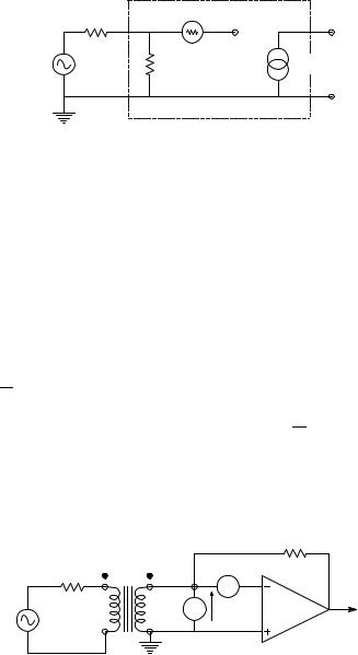
c.Find a numerical value for the transformer’s turns ratio, no, will maximize SNRout. Let 4kT = 1.66 ∞ 10−20; RF = 105 Ω; ena = 3 nVRMS/ Hz (white); ina = 0.4 pARMS/ Hz (white); Rs = 50 Ω; and the noise bandwidth B = 104 Hz.
RF @ T
Rs @ T |
ena |
|
Vi’ |
||
|
ina |
OP-27 |
Vo |
Vs
1: n
FIGURE P9.15
9.16Signal averaging: a periodically evoked transient signal, which can be
modeled by s(t) = (Vso/2)[1 + sin(2π t/T)] for 3T/4 ≤ t ≤ 7T/4, 0 elsewhere, is added to Gaussian broad-band noise having zero mean and variance, σn2. Assume the averager is noiseless (σa2 = 0) and the signal is deterministic so its variance, σs2 = 0.
© 2004 by CRC Press LLC
Noise and the Design of Low-Noise Amplifiers for Biomedical Applications |
389 |
a.Find an algebraic expression for the number of averages, N, required to get a specified MS SNRout > 1 at the peak of the signal.
b.Evaluate N numerically so that when (Vso/2) = 1 μV and σn = 10 μVRMS, the MS SNRout at peak s(t) will be 10.
© 2004 by CRC Press LLC