

- •Analysis and Application of Analog Electronic Circuits to Biomedical Instrumentation
- •Dedication
- •Preface
- •Reader Background
- •Rationale
- •Description of the Chapters
- •Features
- •The Author
- •Table of Contents
- •1.1 Introduction
- •1.2 Sources of Endogenous Bioelectric Signals
- •1.3 Nerve Action Potentials
- •1.4 Muscle Action Potentials
- •1.4.1 Introduction
- •1.4.2 The Origin of EMGs
- •1.5 The Electrocardiogram
- •1.5.1 Introduction
- •1.6 Other Biopotentials
- •1.6.1 Introduction
- •1.6.2 EEGs
- •1.6.3 Other Body Surface Potentials
- •1.7 Discussion
- •1.8 Electrical Properties of Bioelectrodes
- •1.9 Exogenous Bioelectric Signals
- •1.10 Chapter Summary
- •2.1 Introduction
- •2.2.1 Introduction
- •2.2.4 Schottky Diodes
- •2.3.1 Introduction
- •2.4.1 Introduction
- •2.5.1 Introduction
- •2.5.5 Broadbanding Strategies
- •2.6 Photons, Photodiodes, Photoconductors, LEDs, and Laser Diodes
- •2.6.1 Introduction
- •2.6.2 PIN Photodiodes
- •2.6.3 Avalanche Photodiodes
- •2.6.4 Signal Conditioning Circuits for Photodiodes
- •2.6.5 Photoconductors
- •2.6.6 LEDs
- •2.6.7 Laser Diodes
- •2.7 Chapter Summary
- •Home Problems
- •3.1 Introduction
- •3.2 DA Circuit Architecture
- •3.4 CM and DM Gain of Simple DA Stages at High Frequencies
- •3.4.1 Introduction
- •3.5 Input Resistance of Simple Transistor DAs
- •3.7 How Op Amps Can Be Used To Make DAs for Medical Applications
- •3.7.1 Introduction
- •3.8 Chapter Summary
- •Home Problems
- •4.1 Introduction
- •4.3 Some Effects of Negative Voltage Feedback
- •4.3.1 Reduction of Output Resistance
- •4.3.2 Reduction of Total Harmonic Distortion
- •4.3.4 Decrease in Gain Sensitivity
- •4.4 Effects of Negative Current Feedback
- •4.5 Positive Voltage Feedback
- •4.5.1 Introduction
- •4.6 Chapter Summary
- •Home Problems
- •5.1 Introduction
- •5.2.1 Introduction
- •5.2.2 Bode Plots
- •5.5.1 Introduction
- •5.5.3 The Wien Bridge Oscillator
- •5.6 Chapter Summary
- •Home Problems
- •6.1 Ideal Op Amps
- •6.1.1 Introduction
- •6.1.2 Properties of Ideal OP Amps
- •6.1.3 Some Examples of OP Amp Circuits Analyzed Using IOAs
- •6.2 Practical Op Amps
- •6.2.1 Introduction
- •6.2.2 Functional Categories of Real Op Amps
- •6.3.1 The GBWP of an Inverting Summer
- •6.4.3 Limitations of CFOAs
- •6.5 Voltage Comparators
- •6.5.1 Introduction
- •6.5.2. Applications of Voltage Comparators
- •6.5.3 Discussion
- •6.6 Some Applications of Op Amps in Biomedicine
- •6.6.1 Introduction
- •6.6.2 Analog Integrators and Differentiators
- •6.7 Chapter Summary
- •Home Problems
- •7.1 Introduction
- •7.2 Types of Analog Active Filters
- •7.2.1 Introduction
- •7.2.3 Biquad Active Filters
- •7.2.4 Generalized Impedance Converter AFs
- •7.3 Electronically Tunable AFs
- •7.3.1 Introduction
- •7.3.3 Use of Digitally Controlled Potentiometers To Tune a Sallen and Key LPF
- •7.5 Chapter Summary
- •7.5.1 Active Filters
- •7.5.2 Choice of AF Components
- •Home Problems
- •8.1 Introduction
- •8.2 Instrumentation Amps
- •8.3 Medical Isolation Amps
- •8.3.1 Introduction
- •8.3.3 A Prototype Magnetic IsoA
- •8.4.1 Introduction
- •8.6 Chapter Summary
- •9.1 Introduction
- •9.2 Descriptors of Random Noise in Biomedical Measurement Systems
- •9.2.1 Introduction
- •9.2.2 The Probability Density Function
- •9.2.3 The Power Density Spectrum
- •9.2.4 Sources of Random Noise in Signal Conditioning Systems
- •9.2.4.1 Noise from Resistors
- •9.2.4.3 Noise in JFETs
- •9.2.4.4 Noise in BJTs
- •9.3 Propagation of Noise through LTI Filters
- •9.4.2 Spot Noise Factor and Figure
- •9.5.1 Introduction
- •9.6.1 Introduction
- •9.7 Effect of Feedback on Noise
- •9.7.1 Introduction
- •9.8.1 Introduction
- •9.8.2 Calculation of the Minimum Resolvable AC Input Voltage to a Noisy Op Amp
- •9.8.5.1 Introduction
- •9.8.5.2 Bridge Sensitivity Calculations
- •9.8.7.1 Introduction
- •9.8.7.2 Analysis of SNR Improvement by Averaging
- •9.8.7.3 Discussion
- •9.10.1 Introduction
- •9.11 Chapter Summary
- •Home Problems
- •10.1 Introduction
- •10.2 Aliasing and the Sampling Theorem
- •10.2.1 Introduction
- •10.2.2 The Sampling Theorem
- •10.3 Digital-to-Analog Converters (DACs)
- •10.3.1 Introduction
- •10.3.2 DAC Designs
- •10.3.3 Static and Dynamic Characteristics of DACs
- •10.4 Hold Circuits
- •10.5 Analog-to-Digital Converters (ADCs)
- •10.5.1 Introduction
- •10.5.2 The Tracking (Servo) ADC
- •10.5.3 The Successive Approximation ADC
- •10.5.4 Integrating Converters
- •10.5.5 Flash Converters
- •10.6 Quantization Noise
- •10.7 Chapter Summary
- •Home Problems
- •11.1 Introduction
- •11.2 Modulation of a Sinusoidal Carrier Viewed in the Frequency Domain
- •11.3 Implementation of AM
- •11.3.1 Introduction
- •11.3.2 Some Amplitude Modulation Circuits
- •11.4 Generation of Phase and Frequency Modulation
- •11.4.1 Introduction
- •11.4.3 Integral Pulse Frequency Modulation as a Means of Frequency Modulation
- •11.5 Demodulation of Modulated Sinusoidal Carriers
- •11.5.1 Introduction
- •11.5.2 Detection of AM
- •11.5.3 Detection of FM Signals
- •11.5.4 Demodulation of DSBSCM Signals
- •11.6 Modulation and Demodulation of Digital Carriers
- •11.6.1 Introduction
- •11.6.2 Delta Modulation
- •11.7 Chapter Summary
- •Home Problems
- •12.1 Introduction
- •12.2.1 Introduction
- •12.2.2 The Analog Multiplier/LPF PSR
- •12.2.3 The Switched Op Amp PSR
- •12.2.4 The Chopper PSR
- •12.2.5 The Balanced Diode Bridge PSR
- •12.3 Phase Detectors
- •12.3.1 Introduction
- •12.3.2 The Analog Multiplier Phase Detector
- •12.3.3 Digital Phase Detectors
- •12.4 Voltage and Current-Controlled Oscillators
- •12.4.1 Introduction
- •12.4.2 An Analog VCO
- •12.4.3 Switched Integrating Capacitor VCOs
- •12.4.6 Summary
- •12.5 Phase-Locked Loops
- •12.5.1 Introduction
- •12.5.2 PLL Components
- •12.5.3 PLL Applications in Biomedicine
- •12.5.4 Discussion
- •12.6 True RMS Converters
- •12.6.1 Introduction
- •12.6.2 True RMS Circuits
- •12.7 IC Thermometers
- •12.7.1 Introduction
- •12.7.2 IC Temperature Transducers
- •12.8 Instrumentation Systems
- •12.8.1 Introduction
- •12.8.5 Respiratory Acoustic Impedance Measurement System
- •12.9 Chapter Summary
- •References

282 |
Analysis and Application of Analog Electronic Circuits |
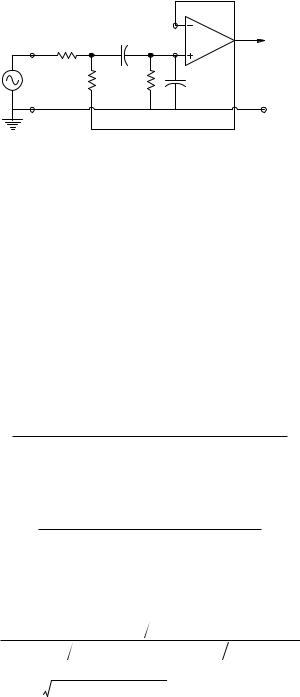
Analog active filters use feedback around op amps to realize desired transfer functions for applications such as band-pass and low-pass filtering to improve signal-to-noise ratios. AFs use only capacitors and resistors in their circuits. Inductors are not used because they are generally large, heavy, and imperfect, i.e., they have significant losses from coil resistance and other factors. AFs are also used to realize sharp cut-off low-pass filters (LPFs) for anti-aliasing filtering of analog signals before periodic, analog-to-digital conversion (sampling). Active notch filters are often used to eliminate the coherent interference that accompanies ECG, EMG, and EEG signals.
Some disconcerting news is that since EEs first discovered that op amps can be used to realize filters, a plethora of different AF design architectures have been developed. In, fact, several excellent texts have been written on the specialized art of active filter design (Schaumann and Van Valkenburg, 2001; Lancaster, 1996; Huelsman, 1993; Deliyannis, Sun, and Fidler, 1998). In some AF designs, filter parameters such as mid-band gain, break frequency, Q, or damping factor cannot be designed for with unique R and C components. For example, all the filter’s Rs and Cs interact, so no single component or set of components can independently determine mid-band gain, break frequency, etc.
The good news is that high-order active filters are generally designed on a modular cascaded basis using certain preferred circuit architectures that allow exact pole and zero placement in the s-plane by simple component value choice. Some examples of these preferred AF architectures will be examined, beginning with the simple controlled-source, Sallen and Key quadratic low-pass filter.
7.2Types of Analog Active Filters
7.2.1Introduction
In the AF designs described next, the op amps will be assumed to be ideal. For serious design evaluation, computer modeling must be used with op amp dynamic models. Note that a filter’s transient response can be just as important as its frequency response. The band-pass filtering of an ECG signal is an example of a biomedical application of an active filter that is transient response sensitive. The fidelity of the sharp QRS spike must be preserved for diagnosis; there must be little rounding of the R-peak and no transient “ringing” following the QRS spike. The linear phase Bessel filter is one class of AF that is free from ringing and suitable for conditioning ECG signals. The exact position of the poles of a high-order (n > 2) Bessel filter determine its characteristics; this filter will be examined in detail later.
© 2004 by CRC Press LLC
Analog Active Filters |
283 |
|
|
|
R |
V3 |
RF |
|
|
|
|
|
Vo |
|
G1 |
V1 |
G2 |
V2 |
IOA |
|
Vo = KvV2 |
||||
|
|
|
|
|
|
+ |
|
|
|
|
Kv = (1 + RF /R) |
|
|
|
|
|
|
Vs |
C1 |
|
C2 |
|
|
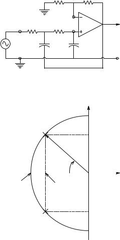
FIGURE 7.1
A Sallen and Key quadratic low-pass filter.
|
|
Imaginary |
|
|
jωn |
|
C-C root |
_____ |
|
jωn√1 − ξ2 |
|
|
ωn |
|
|
|
s-plane |
|
ξ = cosθ |
|
|
θ |
Real |
|
|
|
−ωn |
− ωnξ |
|
|
|
− jωn
FIGURE 7.2
Complex-conjugate pole geometry in the s-plane, showing the relations between pole positions and the natural frequency and damping factor.
7.2.2Sallen and Key Controlled-Source AFs
A basic filter building-block for AFs is the Sallen and Key (S & K), quadratic (two-pole), controlled source (VCVS) architecture. S & K AFs can be cascaded to make high-order low-pass, high-pass, or band-pass filters.
A low-pass S & K filter is shown in Figure 7.1. S & K AFs are quadratic filters, i.e., they generally have a pair of complex-conjugate (C-C) poles, as shown in Figure 7.2. Their transfer function denominators are of the form
© 2004 by CRC Press LLC
284 |
Analysis and Application of Analog Electronic Circuits |
s2 + s2ξωn + ωn2 (in Laplace format). The real part of the C-C poles is negative (−ξωn) and the imaginary parts are ±jωn 1 – ξ2. ωn is called the undamped
natural frequency (in radians/sec) and ξ is the damping factor. For C-C poles, 0 < ξ < 1. The damping factor is the cosine of the angle between the negative real axis in the s-plane and the vector connecting the origin with the upper pole. The closer the poles are to the jω axis, the less damped is the output response of the filter to transient inputs. Also, LPFs with low damping exhibit a peak in their steady-state sinusoidal frequency response (Bode magnitude response) around ωn.
To find the S & K LPF’s transfer function, write node equations for the V1 and V2 nodes:
V1[G1 + G2 + sC1]− V2 G2 − Vo sC1 = Vs G1 |
(7.1A) |
−V1 G2 + V2 [G2 + sC2 ]= 0 |
(7.1B) |
Now V2 can be replaced with Vo/Kv and the node equations rearranged:
V1 [G1 + G2 + sC1]− Vo [sC1 + G2 |
Kv ]= Vs G1 |
(7.2A) |
−V1 G2 + Vo [G2 + sC2 ] Kv |
= 0 |
(7.2B) |
Using Cramer’s rule, it is possible to solve for Vo:
= s2 C C |
K |
v |
+ s C G |
K |
v |
+ C G |
K |
v |
+ C G |
K |
v |
− C G |
] |
+ G 2 |
K |
v |
(7.3) |
1 2 |
|
[ 2 1 |
|
2 2 |
|
1 2 |
|
1 2 |
2 |
|
|
||||||
|
|
|
|
|
|
Vo = + Vs G1 G2 |
|
|
|
|
|
|
|
(7.4) |
|||
Thus, the LPF’s transfer function can be written:
Vo |
(s) = |
|
|
|
|
|
G1 G2 |
|
|
|
|
|
|
(7.5) |
|
V |
2 |
C C K |
|
+ s C G K |
|
|
+ C G K |
|
− C G |
] |
+ G G K |
|
|||
|
s |
v |
v |
+ C G K |
v |
v |
v |
||||||||
s |
|
|
1 2 |
[ 2 1 |
2 2 |
1 2 |
1 2 |
1 2 |
|||||||
Now multiply top and bottom by R1R2 Kv to put the filter’s transfer function in time-constant form:
Vo |
(s) = |
Kv |
|
|
|
s2C1C2R1R2 + s[R1C2 + R2C2 + C1R1 |
(1− Kv )]+ 1 |
(7.6) |
|
Vs |
The denominator of the S & K AF’s transfer function can be written in the standard underdamped quadratic form: s2/ωn2 + s 2 ξ/ωn + 1. By inspection, ωn = 1/ R1 R2 C1 C2 r/s. The filter’s dc gain is Kv, and its damping factor is:
© 2004 by CRC Press LLC
Analog Active Filters |
285 |
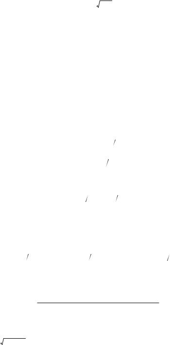
R V3 RF
Vo
C1 |
V1 C2 |
IOA |
V2 |
||
+ |
|
|
Vs |
G1 |
G2 |
|
|
FIGURE 7.3
A Sallen and Key quadratic high-pass filter.
ξ = |
[C2 (R1 |
+ R2 )+ C1R1 |
(1− Kv )] |
(7.7) |
|
|
|
2 R1R2C1C2
For reasons of simplicity, practical S & K active LPF design generally sets Kv = 1 and R1 + R2 = R. Under these conditions, the damping factor is set by the ratio of the capacitor values:
ξ = (C2 C1) |
(7.8) |
The dc gain is unity and the undamped natural frequency is:
ωn = 1 (R C1C2 ) r s |
(7.9) |
To execute an S & K LPF design, given a ωn and damping factor ξ, first set C2/C1, then pick absolute values for C1 and C2 and set R to get the desired ωn. Several S & K LPFs can be cascaded to create a high-order LPF. Pole pair positions in the s-plane can individually be controlled (ξk, ωnk) to realize a specific filter category such as Butterworth, Bessel, Chebychev, etc.
Next, consider the design of the S & K high-pass filter, shown in Figure 7.3. Analysis proceeds in the same manner used for the S & K LPF, except that it is assumed that Kv = 1 to begin; thus, V2 = Vo. The node equations are:
V1[G1 + s(C1 + C2 )]− Vo[G1 + sC2 ] = VssC1 |
(7.10A) |
−V1sC2 + Vo[G2 + sC2 ] = 0 |
(7.10B) |
© 2004 by CRC Press LLC
286 |
Analysis and Application of Analog Electronic Circuits |
Thus,
= G1G2 + sC2C1 + sC1G2 + sC2G2 + s2C1C2 + s2C22 − sC2G1 − s2C22
(7.11)
= G1G2 + s[C1G2 + C2G2 ]+ s2[C1C2 ]
and:
V |
= V |
s |
s2 C |
C |
2 |
(7.12) |
o |
|
1 |
|
|
The S & K HPF transfer function is thus:
Vo |
(s) = |
|
|
|
|
|
|
s2C1C2 |
|
|
(7.13) |
|
V |
s |
2 |
[ |
C C |
] |
|
|
] |
|
|||
|
|
+ s C G |
+ C G |
+ G G |
||||||||
s |
|
|
|
1 2 |
[ |
1 2 |
2 2 |
1 2 |
|
|||
When top and bottom are multiplied by R1R2,
V |
(s) = |
s2C C R R |
|
(7.14) |
o |
1 2 1 2 |
|
||
|
s2C2C1R1R2 + sR1[C1 + C2 |
]+ 1 |
||
Vs |
Now if C1 = C2 = C, the final form of the HPF transfer function is obtained:
|
V |
(s) = |
s2C2R R |
|
(7.15) |
|
|
o |
|
1 2 |
|
||
|
V |
s2C2R R |
+ sR |
2C + 1 |
||
|
s |
1 2 |
1 |
|
|
|
where ωnh = 1/[C R1R2] r/s, and ξh = |
R1R2. |
|
|
|||
An S & K LPF put in series with an S & K HPF yields a fourth-order bandpass filter with two low-frequency C-C poles at ωnh, a mid-band gain of 1,
and a pair of C-C poles from the LPF at ωnlo. Clearly, ωnh < ωnlo. (The BPF is fourth order because it has four poles.) The damping factors, ξh and ξlo,
determine the amount of ringing or transient settling time when the BPF is presented with a transient input such as an ECG QRS spike. ξ is usually set between 0.707 and 0.5.
A final S & K filter to consider is the quadratic BPF shown in Figure 7.4. The filter’s transfer function is found by first writing the node equations on
the V1 and V2 = Vo nodes: |
|
V1[G1 + G3 + sC1]− Vo[G3 + sC1]= Vs G1 |
(7.16A) |
−V1 sC1 + Vo [G2 + s(C1 + C2 )]= 0 |
(7.16B) |
© 2004 by CRC Press LLC
Analog Active Filters |
|
|
287 |
|
|
|
Vo |
G1 |
V1 C1 |
|
IOA |
|
V2 |
||
+ |
|
|
|
Vs |
G3 |
G2 |
C2 |
FIGURE 7.4
A Sallen and Key quadratic band-pass filter.
The determinant is:
=G1G2 + sC1G1 + sC2G1 + G3G2 + sC1G3 + sC2G3 + sC1G2
+s2C12 + s2C1C2 − sC1G3 − s2C12
=G2 (G1 + G3 )+ s[C1(G1 + G2 )+ C2 (G1 + G3 )]+ s2C1C2
and Vo is found from:
Vo = Vs s C1G1
The BP transfer function is written first as:
Vo |
(s) = |
sC1G1 |
|
|
s2C1C2 + s[C1(G1 + G2 )+ C2 (G1 + G3 )]+ G2 |
(G1 + G3 ) |
|
Vs |
(7.17)
(7.18)
(7.19)
To simplify, let C1 = C2 = C and multiply top and bottom by R1 R2 R3:
Vo |
(s) = |
sC R2R3 |
|
(7.20) |
|
s2C2R1R2R3 + sC R2[2R3 + R1 |
]+ (R3 + R1) |
||
Vs |
Next, to put the transfer function in time-constant form, divide top and bottom by (R3 + R1):
V |
(s) = |
|
sC R2R3 (R3 + R1) |
|
o |
|
(R3 + R1)+ sCR2[(2R3 + R1) (R3 + R1)]+ 1 |
(7.21) |
|
Vs |
s2C2 R1R2R3 |
The filter’s ωn = 1/[C (R1R2R3 ) ♣ (R3 + R1 )] r/s; its peak gain at ω = ωn is R3/(2 R3 + R1) and the BPF’s Q is:
© 2004 by CRC Press LLC