

- •Analysis and Application of Analog Electronic Circuits to Biomedical Instrumentation
- •Dedication
- •Preface
- •Reader Background
- •Rationale
- •Description of the Chapters
- •Features
- •The Author
- •Table of Contents
- •1.1 Introduction
- •1.2 Sources of Endogenous Bioelectric Signals
- •1.3 Nerve Action Potentials
- •1.4 Muscle Action Potentials
- •1.4.1 Introduction
- •1.4.2 The Origin of EMGs
- •1.5 The Electrocardiogram
- •1.5.1 Introduction
- •1.6 Other Biopotentials
- •1.6.1 Introduction
- •1.6.2 EEGs
- •1.6.3 Other Body Surface Potentials
- •1.7 Discussion
- •1.8 Electrical Properties of Bioelectrodes
- •1.9 Exogenous Bioelectric Signals
- •1.10 Chapter Summary
- •2.1 Introduction
- •2.2.1 Introduction
- •2.2.4 Schottky Diodes
- •2.3.1 Introduction
- •2.4.1 Introduction
- •2.5.1 Introduction
- •2.5.5 Broadbanding Strategies
- •2.6 Photons, Photodiodes, Photoconductors, LEDs, and Laser Diodes
- •2.6.1 Introduction
- •2.6.2 PIN Photodiodes
- •2.6.3 Avalanche Photodiodes
- •2.6.4 Signal Conditioning Circuits for Photodiodes
- •2.6.5 Photoconductors
- •2.6.6 LEDs
- •2.6.7 Laser Diodes
- •2.7 Chapter Summary
- •Home Problems
- •3.1 Introduction
- •3.2 DA Circuit Architecture
- •3.4 CM and DM Gain of Simple DA Stages at High Frequencies
- •3.4.1 Introduction
- •3.5 Input Resistance of Simple Transistor DAs
- •3.7 How Op Amps Can Be Used To Make DAs for Medical Applications
- •3.7.1 Introduction
- •3.8 Chapter Summary
- •Home Problems
- •4.1 Introduction
- •4.3 Some Effects of Negative Voltage Feedback
- •4.3.1 Reduction of Output Resistance
- •4.3.2 Reduction of Total Harmonic Distortion
- •4.3.4 Decrease in Gain Sensitivity
- •4.4 Effects of Negative Current Feedback
- •4.5 Positive Voltage Feedback
- •4.5.1 Introduction
- •4.6 Chapter Summary
- •Home Problems
- •5.1 Introduction
- •5.2.1 Introduction
- •5.2.2 Bode Plots
- •5.5.1 Introduction
- •5.5.3 The Wien Bridge Oscillator
- •5.6 Chapter Summary
- •Home Problems
- •6.1 Ideal Op Amps
- •6.1.1 Introduction
- •6.1.2 Properties of Ideal OP Amps
- •6.1.3 Some Examples of OP Amp Circuits Analyzed Using IOAs
- •6.2 Practical Op Amps
- •6.2.1 Introduction
- •6.2.2 Functional Categories of Real Op Amps
- •6.3.1 The GBWP of an Inverting Summer
- •6.4.3 Limitations of CFOAs
- •6.5 Voltage Comparators
- •6.5.1 Introduction
- •6.5.2. Applications of Voltage Comparators
- •6.5.3 Discussion
- •6.6 Some Applications of Op Amps in Biomedicine
- •6.6.1 Introduction
- •6.6.2 Analog Integrators and Differentiators
- •6.7 Chapter Summary
- •Home Problems
- •7.1 Introduction
- •7.2 Types of Analog Active Filters
- •7.2.1 Introduction
- •7.2.3 Biquad Active Filters
- •7.2.4 Generalized Impedance Converter AFs
- •7.3 Electronically Tunable AFs
- •7.3.1 Introduction
- •7.3.3 Use of Digitally Controlled Potentiometers To Tune a Sallen and Key LPF
- •7.5 Chapter Summary
- •7.5.1 Active Filters
- •7.5.2 Choice of AF Components
- •Home Problems
- •8.1 Introduction
- •8.2 Instrumentation Amps
- •8.3 Medical Isolation Amps
- •8.3.1 Introduction
- •8.3.3 A Prototype Magnetic IsoA
- •8.4.1 Introduction
- •8.6 Chapter Summary
- •9.1 Introduction
- •9.2 Descriptors of Random Noise in Biomedical Measurement Systems
- •9.2.1 Introduction
- •9.2.2 The Probability Density Function
- •9.2.3 The Power Density Spectrum
- •9.2.4 Sources of Random Noise in Signal Conditioning Systems
- •9.2.4.1 Noise from Resistors
- •9.2.4.3 Noise in JFETs
- •9.2.4.4 Noise in BJTs
- •9.3 Propagation of Noise through LTI Filters
- •9.4.2 Spot Noise Factor and Figure
- •9.5.1 Introduction
- •9.6.1 Introduction
- •9.7 Effect of Feedback on Noise
- •9.7.1 Introduction
- •9.8.1 Introduction
- •9.8.2 Calculation of the Minimum Resolvable AC Input Voltage to a Noisy Op Amp
- •9.8.5.1 Introduction
- •9.8.5.2 Bridge Sensitivity Calculations
- •9.8.7.1 Introduction
- •9.8.7.2 Analysis of SNR Improvement by Averaging
- •9.8.7.3 Discussion
- •9.10.1 Introduction
- •9.11 Chapter Summary
- •Home Problems
- •10.1 Introduction
- •10.2 Aliasing and the Sampling Theorem
- •10.2.1 Introduction
- •10.2.2 The Sampling Theorem
- •10.3 Digital-to-Analog Converters (DACs)
- •10.3.1 Introduction
- •10.3.2 DAC Designs
- •10.3.3 Static and Dynamic Characteristics of DACs
- •10.4 Hold Circuits
- •10.5 Analog-to-Digital Converters (ADCs)
- •10.5.1 Introduction
- •10.5.2 The Tracking (Servo) ADC
- •10.5.3 The Successive Approximation ADC
- •10.5.4 Integrating Converters
- •10.5.5 Flash Converters
- •10.6 Quantization Noise
- •10.7 Chapter Summary
- •Home Problems
- •11.1 Introduction
- •11.2 Modulation of a Sinusoidal Carrier Viewed in the Frequency Domain
- •11.3 Implementation of AM
- •11.3.1 Introduction
- •11.3.2 Some Amplitude Modulation Circuits
- •11.4 Generation of Phase and Frequency Modulation
- •11.4.1 Introduction
- •11.4.3 Integral Pulse Frequency Modulation as a Means of Frequency Modulation
- •11.5 Demodulation of Modulated Sinusoidal Carriers
- •11.5.1 Introduction
- •11.5.2 Detection of AM
- •11.5.3 Detection of FM Signals
- •11.5.4 Demodulation of DSBSCM Signals
- •11.6 Modulation and Demodulation of Digital Carriers
- •11.6.1 Introduction
- •11.6.2 Delta Modulation
- •11.7 Chapter Summary
- •Home Problems
- •12.1 Introduction
- •12.2.1 Introduction
- •12.2.2 The Analog Multiplier/LPF PSR
- •12.2.3 The Switched Op Amp PSR
- •12.2.4 The Chopper PSR
- •12.2.5 The Balanced Diode Bridge PSR
- •12.3 Phase Detectors
- •12.3.1 Introduction
- •12.3.2 The Analog Multiplier Phase Detector
- •12.3.3 Digital Phase Detectors
- •12.4 Voltage and Current-Controlled Oscillators
- •12.4.1 Introduction
- •12.4.2 An Analog VCO
- •12.4.3 Switched Integrating Capacitor VCOs
- •12.4.6 Summary
- •12.5 Phase-Locked Loops
- •12.5.1 Introduction
- •12.5.2 PLL Components
- •12.5.3 PLL Applications in Biomedicine
- •12.5.4 Discussion
- •12.6 True RMS Converters
- •12.6.1 Introduction
- •12.6.2 True RMS Circuits
- •12.7 IC Thermometers
- •12.7.1 Introduction
- •12.7.2 IC Temperature Transducers
- •12.8 Instrumentation Systems
- •12.8.1 Introduction
- •12.8.5 Respiratory Acoustic Impedance Measurement System
- •12.9 Chapter Summary
- •References
314 |
Analysis and Application of Analog Electronic Circuits |
||
|
Vs’ |
|
|
|
IOA |
V3’ |
|
|
V2’ |
R4’ |
|
|
|
|
|
|
R2’ |
R3’ |
|
|
R1’ |
|
|
|
Vc |
IOA |
Vo |
|
R1 |
R3 |
|
|
|
|
|
|
R2 |
(DA) |
|
|
|
R4 |
|
|
V2 |
|
|
|
IOA |
V3 |
|
|
Vs |
|
|
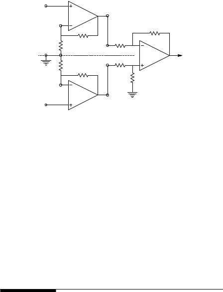
FIGURE 8.2
The three-op amp instrumentation amplifier.
asymptotically to that of the input transistors. This has three important advantages: (a) open-loop gain is boosted for increasing programmed gain, thus reducing gain-related errors. (b) The gain-bandwidth product (determined by C1, C2, and the preamp transconductance) increases with programmed gain, thus optimizing frequency response. (c) The input voltage noise is reduced to a value of 9 nV/ Hz, determined mainly by the collector current and base resistance of the input devices.
It is clear that the AD620 has many features that make it outperform the simple three-op amp IA shown in Figure 8.2. Given proper ohmic isolation,
the AD620 can make an effective ECG amplifier. It can be run on batteries as low as ±2.3 V and its output can modulate a voltage-to-frequency con-
verter (VFC), also battery powered, generating NBFM. The VFC’s digital output can be coupled to the nonisolated world through a photo-optic coupler and thus be demodulated by conventional means, filtered, and further amplified.
8.3Medical Isolation Amps
8.3.1Introduction
All amplifiers used to record biopotential signals from humans (ECG, EEG, EMG, EOG, etc.) must meet certain safety standards for worst-case voltage breakdown and maximum leakage currents through their input leads attached to electrodes on the body, and maximum current through any
© 2004 by CRC Press LLC
Instrumentation and Medical Isolation Amplifiers |
315 |
driven output lead attached to the body. A variety of testing conditions or scenarios to ensure patient safety have been formulated by various regulatory agencies. The conservative leakage current and voltage breakdown criteria set by the National Fire Protection Association (NFPA; Quincy, MA) and the Association for the Advancement of Medical Instrumentation (AAMI) have generally been adopted by medical equipment manufacturers in the U.S. and by U.S. hospitals and other health care facilities. A number of other regulatory agencies also are involved in formulating and adopting electrical medical safety standards:
•International Electrotechnical Commission (IEC)
•Underwriters Laboratories (UL)
•Health Industries Manufacturers’ Association (HEMA)
•National Electrical Manufacturers’ Association (NEMA)
•U.S. Food and Drug Administration (FDA)
Most of the standards have been adopted to prevent patient electrocution, including burns, induction of fibrillation in the heart, pain, muscle spasms, etc.
Space does not permit detailing the effects of electroshock and the many scenarios by which it can occur. Nor can the technology of safe grounding practices and ground fault interruption be explored. The interested reader should consult Chapter 14 in Webster (1992) for comprehensive treatment of these details.
If the threshold ac heart surface current required to induce cardiac fibrillation in 50% of dogs tested is plotted vs. frequency, it is seen that the least current is required between 40 to 100 Hz. From 80 to 600 μA RMS of 60 Hz, current will induce cardiac fibrillation when applied directly to the heart, as through a catheter (Webster, 1992). Thus, the NFPA–ANSI/AAMI standard for ECG amplifier lead leakage is that isolated input lead current (at 60 Hz) must be <10 μA between any two leads shorted together and <10 μA for any input lead connected to the power plug ground (green wire) with and without the amplifier’s case grounded. A more severe test is that isolation amplifier input lead leakage current must be <20 μA when any input lead is connected to the high side of the 120 Vac mains. The medical isolation amplifier has evolved to meet these severe tests for leakage.
Isolation is accomplished by electrically separating the input stage of the isolation amplifier (IsoA) from the output stage. That is, the input stage has a separate floating power supply and a “ground” that are connected to the output side of the IsoA by a resistance of over 1000 megohms, and a parallel capacitance in the low picofarad range. The signal input terminals of the input stage are isolated from the IsoA’s output by a similar very high impedance, although the Thevenin output resistance of the IsoA can range from milliohms to several hundred ohms.
© 2004 by CRC Press LLC
316 |
Analysis and Application of Analog Electronic Circuits |
8.3.2Common Types of Medical Isolation Amplifiers
Current practice uses three major means of effecting the Galvanic isolation of the input and output stages of IsoAs. The first means is to use a high-quality toroidal transformer to magnetically couple regulated, high-frequency ac power from the output side to the isolated input stage where it is rectified and filtered; it is also coupled to rectifiers and filters serving the output amplifiers. Frequencies in the range of 50 to 500 kHz are typically used with transformer isolation IsoAs. The output signal from the isolated headstage modulates an ac carrier magnetically coupled to a demodulator on the output side. Transformer coupling can provide 12to 16-bit resolution and bandwidths up to 75 kHz. Galvanic isolation with transformers is excellent; their maximum breakdown voltage can be made as high as 10 kV, but is often much lower.
A second means of isolation is to use photo-optic coupling of the amplified signal; usually pulse-width or delta–sigma modulation of the optical signal is used, although direct linear analog photo-optic coupling can be used. In the optical type of IsoA, a separate isolated dc–dc converter must be used to power the input stage. Photo-optic couplers can be made to withstand voltages in the 4- to 7-kV range before breakdown.
A third means of isolation is to use a pair of small (e.g., 1 pF) capacitors to couple a pulse-modulated signal from the isolated input to the output stage. A separate isolated power supply must be used with the differential capacitor-coupled IsoA as well. Table 8.1 lists some of the critical specifications of five types of medical-grade IsoAs.
The Burr–Brown ISO121 differential capacitor-coupled IsoA is used with a separate isolated clock to run its duty cycle modulator. The clock frequency can be from 5 to 700 kHz, giving commensurate bandwidths, governed by the Nyquist criterion.
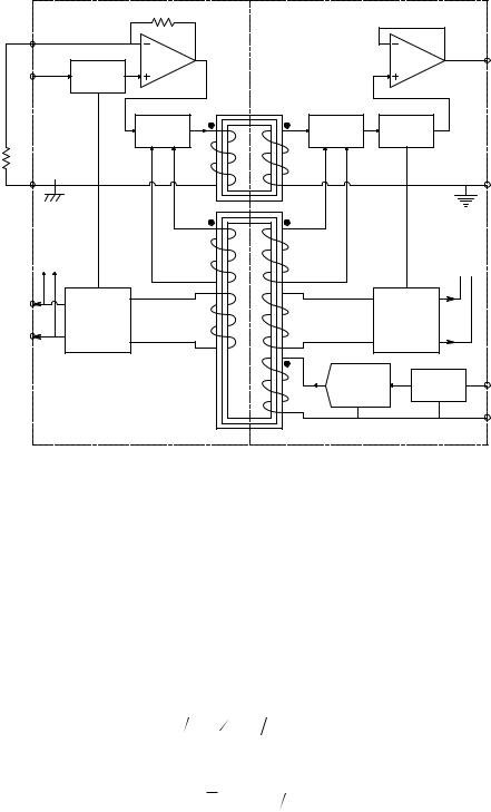
A simplified schematic of an Analog Devices AD289 magnetically coupled IsoA is shown in Figure 8.3. Note that this IsoA has a single-ended input. In this case, an AD620 IA is powered from the AD289’s isolated power supply and provides true isolated differential input to the IsoA that rejects unwanted common-mode noise and interference. The clock power oscillator drives a toroidal core, T1, on which coils for the input and output isolated power supplies are wound and for the synchronizing signal for the double-side- band, suppressed-carrier (DSBSC) modulator and demodulator. A separate toroidal transformer, T2, couples the DSBSCM output signal to the output side of the IsoA. This is basically the architecture used in the Intronics 290 and the Burr–Brown BB3656 IsoAs.
An unmodulated feedback-type analog optical isolation system is used in the Burr–Brown BB3652 differential optically coupled linear IsoA. This IsoA still requires a transformer-isolated power supply for the input headstage and for the driver for the linear optocoupler. A feedback-type linear optocoupler, similar to that used in the BB3652, is shown in Figure 8.4. (In the B3652, OA1 is replaced with a high input impedance DA headstage.) The circuit works in the following manner.
© 2004 by CRC Press LLC

Instrumentation and Medical Isolation Amplifiers
TABLE 8.1
Comparison of Properties of Some Popular Isolation Amplifiers
Amplifier |
IA294 |
BB3656 |
BB3652 |
BB ISO121 |
ISO-Z |
Iso. type |
Transformer |
Transformer |
Optical |
Capacitor |
Transformer? |
Manufacturer |
Intronics |
Burr–Brown |
Burr–Brown |
Burr–Brown |
Dataq |
CMV isolation |
±5000 V |
±3500 V |
±2000 V |
3500 RMS |
1500 V |
|
continuous; |
continuous; |
continuous; |
|
continuous; |
|
±6500 V |
±8000 V, |
±5000 V, |
|
5000 V, 10 sec |
|
10-MS pulse |
10 sec |
10 sec. |
|
|
CMRR @ |
120 dB @ |
108 dB |
80 dB @ 60 Hz |
115 dB IMR @ |
>100 dB @ |
60 Hz |
60 Hz |
|
|
60 Hz |
60 Hz |
Gain range |
10 (fixed) |
1 to 100 |
1 to >100, by |
1 V/V (fixed) |
10 (fixed) |
|
|
|
formula |
Iac = V2πfC; C |
<5 μA, any |
Leakage to |
10 μA max |
0.5 μA |
0.5 μA; 1.8 pF |
||
120 Vac |
|
|
leakage |
2.21 pF |
input to |
mains |
8 μV ppk; |
5 μV pkpk; |
capacitance |
4 μVRMS/ Hz |
ground |
Noise |
8 μV pkpk |
<4 μVRMS, |
|||
|
0.05 to |
0.05 to |
0.05 - 100 Hz |
|
referred to |
|
100 Hz |
100 Hz BW |
BW |
|
input, |
|
|
|
|
|
“wideband” |
Bandwidth |
0 to 1 kHz |
0 to 30 kHz; |
0 - 15 kHz, |
0 to 60 kHz; |
0 to 8 kHz |
|
|
±3 dB |
± 3 dB |
(approx. |
|
|
|
|
1.2 V/μs |
200 kHz clock) |
|
Slew rate |
? |
+0.1, |
2 V/μs |
? |
|
|
|
–0.04 V/μs |
|
|
|
|
|
|
|
|
|
The summing junction of OA2 is at 0 V. DC bias current through RB1, IB1, drives the OA2 output negative, biasing the LED, D2, on at some ID20. D2’s light illuminates photodiodes D1 and D3 equally; the reverse photocurrent through D1 drives OA2’s output positive, reducing ID2. It thus provides a linearizing negative feedback around OA2, acting against the current produced by the input voltage, Vin/R1. Because D1 and D3 are matched photo-diodes, the reverse photocurrent in D3 equals that in D1, i.e., ID10 = ID30 and Vo = R3
(ID30 − IB3). The bias current IB3 makes Vo 0 when Vin = 0. Now when Vin > 0, the input current, Vin/R1, makes the LED D2 brighter, increasing ID1 = ID3 >
ID10 = ID30, increasing Vo. Thus, Vo = KV Vin. Note that analog opto-isolation eliminates the need for a high-frequency carrier, modulation, and demodulation, while giving a very high degree of Galvanic isolation. Unfortunately, the isolated headstage still must receive its power through a magnetically isolated power supply. It could use batteries, however, which would improve its isolation.
IsoAs using capacitor isolation use high-frequency duty-cycle modulation to transmit the signal across the isolation barrier using a differential 1-pF capacitor coupling circuit. This type of IsoA also needs an isolated power supply for the input stages, clock oscillator, and modulator. Figure 8.5 illustrates schematically a simplified version of how the Burr–Brown ISO121 capacitively isolated IsoA works.
© 2004 by CRC Press LLC
318 |
Analysis and Application of Analog Electronic Circuits |
|
10 k |
|
|
Gain set |
|
|
|
Resistor |
|
|
|
|
|
|
IA out |
Input |
OA |
|
OA |
Anti-aliasing |
|
Vo |
|
|
|
||
|
LPF |
|
|
|
|
T2 |
|
|
PSM |
PSD |
LPF |
Rgain
Input
Out. ground
common
Isolated |
Isolated |
|
|
power supply |
power supply |
|
|
± 15 V |
± 15 V |
|
|
Isolated |
|
|
|
± 15V out |
|
|
|
Power |
|
+ |
|
oscillator |
Regulator |
||
|
@ fc
dc power in
T1
FIGURE 8.3
Simplified schematic of an Analog Device’s AD289 magnetically isolated isolation amplifier (IsoA). An AD620 IA is used as a differential front end for the IsoA; it is powered from the AD289’s isolated power supply.
The positive signal Vin is added to a high-frequency symmetrical triangle
wave, VT, with peak height, VpkT. The sum of VT and Vin is passed through a comparator, which generates a variable duty-cycle square wave, V2. Note
that the highest frequency in Vin is fc, the clock frequency, and Vinmax < Vpk. The state transitions in V2 are coupled through the two 1-pF capacitors
as spikes to a flip-flop on the output side of the IA. The flip-flop’s transitions are triggered by the spikes. At the flip flop’s output, a ±V3m-variable dutycycle square wave, V3, is then averaged by low-pass filtering to yield Vo.
The duty cycle of V2 and V3 can be shown to be:
η V |
∫ T |
T = |
1 |
+ V |
2V |
, |
V |
< v |
pkT |
(8.1) |
( in ) |
+ |
|
( 2 |
in |
pkT ) |
|
in |
|
|
The average of the symmetrical flip-flop output is:
Vo = |
V3 = Vin (V3m VpkT ) |
(8.2) |
© 2004 by CRC Press LLC