

- •Analysis and Application of Analog Electronic Circuits to Biomedical Instrumentation
- •Dedication
- •Preface
- •Reader Background
- •Rationale
- •Description of the Chapters
- •Features
- •The Author
- •Table of Contents
- •1.1 Introduction
- •1.2 Sources of Endogenous Bioelectric Signals
- •1.3 Nerve Action Potentials
- •1.4 Muscle Action Potentials
- •1.4.1 Introduction
- •1.4.2 The Origin of EMGs
- •1.5 The Electrocardiogram
- •1.5.1 Introduction
- •1.6 Other Biopotentials
- •1.6.1 Introduction
- •1.6.2 EEGs
- •1.6.3 Other Body Surface Potentials
- •1.7 Discussion
- •1.8 Electrical Properties of Bioelectrodes
- •1.9 Exogenous Bioelectric Signals
- •1.10 Chapter Summary
- •2.1 Introduction
- •2.2.1 Introduction
- •2.2.4 Schottky Diodes
- •2.3.1 Introduction
- •2.4.1 Introduction
- •2.5.1 Introduction
- •2.5.5 Broadbanding Strategies
- •2.6 Photons, Photodiodes, Photoconductors, LEDs, and Laser Diodes
- •2.6.1 Introduction
- •2.6.2 PIN Photodiodes
- •2.6.3 Avalanche Photodiodes
- •2.6.4 Signal Conditioning Circuits for Photodiodes
- •2.6.5 Photoconductors
- •2.6.6 LEDs
- •2.6.7 Laser Diodes
- •2.7 Chapter Summary
- •Home Problems
- •3.1 Introduction
- •3.2 DA Circuit Architecture
- •3.4 CM and DM Gain of Simple DA Stages at High Frequencies
- •3.4.1 Introduction
- •3.5 Input Resistance of Simple Transistor DAs
- •3.7 How Op Amps Can Be Used To Make DAs for Medical Applications
- •3.7.1 Introduction
- •3.8 Chapter Summary
- •Home Problems
- •4.1 Introduction
- •4.3 Some Effects of Negative Voltage Feedback
- •4.3.1 Reduction of Output Resistance
- •4.3.2 Reduction of Total Harmonic Distortion
- •4.3.4 Decrease in Gain Sensitivity
- •4.4 Effects of Negative Current Feedback
- •4.5 Positive Voltage Feedback
- •4.5.1 Introduction
- •4.6 Chapter Summary
- •Home Problems
- •5.1 Introduction
- •5.2.1 Introduction
- •5.2.2 Bode Plots
- •5.5.1 Introduction
- •5.5.3 The Wien Bridge Oscillator
- •5.6 Chapter Summary
- •Home Problems
- •6.1 Ideal Op Amps
- •6.1.1 Introduction
- •6.1.2 Properties of Ideal OP Amps
- •6.1.3 Some Examples of OP Amp Circuits Analyzed Using IOAs
- •6.2 Practical Op Amps
- •6.2.1 Introduction
- •6.2.2 Functional Categories of Real Op Amps
- •6.3.1 The GBWP of an Inverting Summer
- •6.4.3 Limitations of CFOAs
- •6.5 Voltage Comparators
- •6.5.1 Introduction
- •6.5.2. Applications of Voltage Comparators
- •6.5.3 Discussion
- •6.6 Some Applications of Op Amps in Biomedicine
- •6.6.1 Introduction
- •6.6.2 Analog Integrators and Differentiators
- •6.7 Chapter Summary
- •Home Problems
- •7.1 Introduction
- •7.2 Types of Analog Active Filters
- •7.2.1 Introduction
- •7.2.3 Biquad Active Filters
- •7.2.4 Generalized Impedance Converter AFs
- •7.3 Electronically Tunable AFs
- •7.3.1 Introduction
- •7.3.3 Use of Digitally Controlled Potentiometers To Tune a Sallen and Key LPF
- •7.5 Chapter Summary
- •7.5.1 Active Filters
- •7.5.2 Choice of AF Components
- •Home Problems
- •8.1 Introduction
- •8.2 Instrumentation Amps
- •8.3 Medical Isolation Amps
- •8.3.1 Introduction
- •8.3.3 A Prototype Magnetic IsoA
- •8.4.1 Introduction
- •8.6 Chapter Summary
- •9.1 Introduction
- •9.2 Descriptors of Random Noise in Biomedical Measurement Systems
- •9.2.1 Introduction
- •9.2.2 The Probability Density Function
- •9.2.3 The Power Density Spectrum
- •9.2.4 Sources of Random Noise in Signal Conditioning Systems
- •9.2.4.1 Noise from Resistors
- •9.2.4.3 Noise in JFETs
- •9.2.4.4 Noise in BJTs
- •9.3 Propagation of Noise through LTI Filters
- •9.4.2 Spot Noise Factor and Figure
- •9.5.1 Introduction
- •9.6.1 Introduction
- •9.7 Effect of Feedback on Noise
- •9.7.1 Introduction
- •9.8.1 Introduction
- •9.8.2 Calculation of the Minimum Resolvable AC Input Voltage to a Noisy Op Amp
- •9.8.5.1 Introduction
- •9.8.5.2 Bridge Sensitivity Calculations
- •9.8.7.1 Introduction
- •9.8.7.2 Analysis of SNR Improvement by Averaging
- •9.8.7.3 Discussion
- •9.10.1 Introduction
- •9.11 Chapter Summary
- •Home Problems
- •10.1 Introduction
- •10.2 Aliasing and the Sampling Theorem
- •10.2.1 Introduction
- •10.2.2 The Sampling Theorem
- •10.3 Digital-to-Analog Converters (DACs)
- •10.3.1 Introduction
- •10.3.2 DAC Designs
- •10.3.3 Static and Dynamic Characteristics of DACs
- •10.4 Hold Circuits
- •10.5 Analog-to-Digital Converters (ADCs)
- •10.5.1 Introduction
- •10.5.2 The Tracking (Servo) ADC
- •10.5.3 The Successive Approximation ADC
- •10.5.4 Integrating Converters
- •10.5.5 Flash Converters
- •10.6 Quantization Noise
- •10.7 Chapter Summary
- •Home Problems
- •11.1 Introduction
- •11.2 Modulation of a Sinusoidal Carrier Viewed in the Frequency Domain
- •11.3 Implementation of AM
- •11.3.1 Introduction
- •11.3.2 Some Amplitude Modulation Circuits
- •11.4 Generation of Phase and Frequency Modulation
- •11.4.1 Introduction
- •11.4.3 Integral Pulse Frequency Modulation as a Means of Frequency Modulation
- •11.5 Demodulation of Modulated Sinusoidal Carriers
- •11.5.1 Introduction
- •11.5.2 Detection of AM
- •11.5.3 Detection of FM Signals
- •11.5.4 Demodulation of DSBSCM Signals
- •11.6 Modulation and Demodulation of Digital Carriers
- •11.6.1 Introduction
- •11.6.2 Delta Modulation
- •11.7 Chapter Summary
- •Home Problems
- •12.1 Introduction
- •12.2.1 Introduction
- •12.2.2 The Analog Multiplier/LPF PSR
- •12.2.3 The Switched Op Amp PSR
- •12.2.4 The Chopper PSR
- •12.2.5 The Balanced Diode Bridge PSR
- •12.3 Phase Detectors
- •12.3.1 Introduction
- •12.3.2 The Analog Multiplier Phase Detector
- •12.3.3 Digital Phase Detectors
- •12.4 Voltage and Current-Controlled Oscillators
- •12.4.1 Introduction
- •12.4.2 An Analog VCO
- •12.4.3 Switched Integrating Capacitor VCOs
- •12.4.6 Summary
- •12.5 Phase-Locked Loops
- •12.5.1 Introduction
- •12.5.2 PLL Components
- •12.5.3 PLL Applications in Biomedicine
- •12.5.4 Discussion
- •12.6 True RMS Converters
- •12.6.1 Introduction
- •12.6.2 True RMS Circuits
- •12.7 IC Thermometers
- •12.7.1 Introduction
- •12.7.2 IC Temperature Transducers
- •12.8 Instrumentation Systems
- •12.8.1 Introduction
- •12.8.5 Respiratory Acoustic Impedance Measurement System
- •12.9 Chapter Summary
- •References

Noise and the Design of Low-Noise Amplifiers for Biomedical Applications |
357 |
|||||
|
|
= |
AD2 + AC2 |
(ena2 + ina2Rs2 + 4kTR)B MSV |
|
|
|
von2 |
(9.73) |
||||
|
||||||
2 |
|
|
||||
B is the Hertz noise bandwidth of the DA acting on the white PDSs. Now the MS output SNR of the DA for a pure DM input is easily found to be:
SNRo = |
2v 2 |
B |
(9.74) |
sd |
|
||
(1+ CMRR−2 )(ena2 + ina2Rs2 + 4kTRs ) |
|||
Note that CMRR−2 1 and is negligible. The 2 in the numerator is real, however, and illustrates the advantage of using a DA with pure DM signals.
9.7Effect of Feedback on Noise
9.7.1Introduction
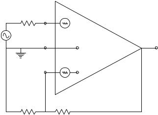
Chapter 4 and Chapter 5 showed that negative voltage feedback (NVFB), correctly applied, has many important beneficial effects in signal conditioning. These include but are not limited to reduction of harmonic distortion, extension of bandwidth, and reduction of output impedance. A common misconception is that negative voltage feedback also acts to improve output SNR and reduce the NF. It will be shown next that NVFB has quite the opposite effect: it reduces the output SNR and increases the NF.
9.7.2Calculation of SNR0 of an Amplifier with NVFB
Figure 9.15 illustrates a noisy differential amplifier with NVFB applied through a voltage divider to the inverting input. To simplify calculations, assume that the DA has a finite difference-mode gain, AD, and an infinite CMRR, i.e., AC 0. Also, neglect the input voltages produced by the current noise sources. The DA’s output is given by:
vo = AD′(vi − vi′)
The noninverting input node signal voltage is vi = vs. node voltage is:
v′ = v |
|
|
R1 |
ˆ |
= v |
β |
o |
|
˜ |
||||
i |
|
o |
|
|||
|
R1 |
+ RF ↓ |
|
|
||
(9.75)
The inverting input
(9.76)
© 2004 by CRC Press LLC
358 |
Analysis and Application of Analog Electronic Circuits |
Rs @ T |
ena |
|
 vi
vi
vs
vo
ena’
vi’
R1 @ T |
RF @ T |
FIGURE 9.15
Circuit model for a DA with negative voltage feedback. The ina s are neglected.
When the expressions for vi and vi′ are substituted into Equation 9.75, vo is found to be:
vo = |
v A′ |
(9.77) |
s D |
||
1+ β A′ |
||
|
D |
|
The mean-squared output signal voltage is thus:
|
|
|
|
|
A′2 |
|
|
2 |
2 |
|
|
|
|
||
|
|
D |
|
|
|||
vos |
= vs |
|
1+ β A′ |
2 |
(9.78) |
||
|
|
|
( |
D ) |
|
|
|
When considering the noises, vs is set to zero and, for the time signals:
v |
o |
= A′ |
[ |
e |
na |
+ e |
ns |
− |
e′ + βv |
o |
+ βe |
nf |
+ (1− β)e |
n1} |
|
(9.79) |
|||||||
|
D |
|
|
|
|
|
{ |
na |
|
|
|
|
|
|
|
||||||||
|
|
|
|
|
|
|
|
|
|
|
|
|
|
|
|
|
|
|
|
] |
|
|
|
The preceding equation is solved for vo(t): |
|
|
|
|
|
|
|
||||||||||||||||
v |
(1+ βA′ ) |
= A′ |
[ |
e |
nn |
+ e |
ns |
− e′ − βe |
nf |
− (1− β)e |
n1 |
] |
(9.80) |
||||||||||
o |
|
|
D |
|
|
D |
|
|
|
|
na |
|
|
|
|
||||||||
Note that β ∫ R1/(R1 + RF) and ena = ena′ statistically but not necessarily in the time domain; ens, en1, and enf = the thermal noise voltages from Rs, R1, and RF, respectively — all at Kelvin temperature T. One can now write the expression for the mean squared vo over the noise Hertz bandwidth B:
© 2004 by CRC Press LLC
Noise and the Design of Low-Noise Amplifiers for Biomedical Applications |
359 |
|||||||||
|
|
|
|
A′2 |
|
[2ena2 + 4kTRs + β2 4kTRF + (1− β) |
2 |
|
]B |
|
von2 = |
|
|
4kTR1 |
(9.81) |
||||||
|
D |
|
|
|||||||
( |
D ) |
2 |
|
|||||||
|
|
|
1 |
+ βA′ |
|
|
|
|
|
|
The MS signal-to-noise ratio of the feedback amplifier is found by taking the ratio of Equation 9.78 to Equation 9.81:
SNRo = |
v 2 |
B |
|
|
s |
|
|
|
|
2 ena2 + 4kT [RS + β2 RF + (1− β)2 R1 |
] |
(9.82) |
||
It is left as an exercise for the reader to show that, in the absence of feedback (no feedback resistors at all), the output SNR is:
SNRo = |
v 2 |
B |
(9.83) |
|
|
s |
|
||
2 e 2 |
+ |
4kTR |
||
|
na |
|
s |
|
Note that the presence of the feedback voltage divider resistors adds noise to the output and gives a lower SNRo. Contemplate the effect of applying feedback through a purely capacitive voltage divider. Capacitors do not generate thermal noise.
9.8Examples of Noise-Limited Resolution of Certain Signal Conditioning Systems
9.8.1Introduction
In following examples, assume that the stationary sources of noise (resistor thermal noise, amplifier ena and ina) are statistically independent, are uncorrelated, have white spectra in the range of frequencies of interest, and are added in the MS sense as PDSs are. Aside from their short-circuit input voltage noise, ena, the op amps are assumed to be ideal.
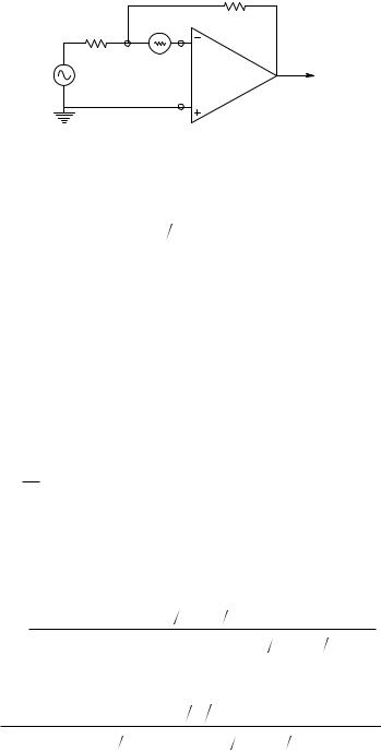
9.8.2Calculation of the Minimum Resolvable AC Input Voltage to a Noisy Op Amp
Figure 9.16 illustrates a simple inverting op amp circuit with a sinusoidal input. Assume that ina RF ena and thus ina produces negligible noise at the amplifier output and is deleted from the model. Only amplifier ena and resistor Johnson noise contribute to the amplifier’s noise output. The meansquared signal output is given by:
© 2004 by CRC Press LLC
360 |
Analysis and Application of Analog Electronic Circuits |
|
|
|
RF @ T |
|
R1 @ T |
ena |
|
|
|
+ |
|
vi’ |
|
|
Vo |
OA
VS
vi
FIGURE 9.16
A simple inverting op amp circuit with a sinusoidal voltage input. White thermal noise is assumed to come from the two resistors and also from the op amp’s ena.
|
= (VS2 2)(−RF R1)2 |
|
vos2 |
(9.84) |
The noise voltages in this circuit are all conditioned by different gains: en1 is the thermal noise from R1; it is conditioned by the same gain as vs, i.e., (–RF/R1). Because the summing junction is at 0 V due to the ideal op amp assumption, the thermal noise in RF, enf, is seen at the output as simply enf (a gain of unity). Again, the gain for ena is found by assuming vi′ = 0. The voltage at the R1–RF node thus must be ena; therefore, the voltage divider ratio gives vo = ena (1 + RF/R1). Note that these three gains are derived assuming ena, enf, and en1 are voltages varying in time. When the MS noise at the output is examined, the gains must be squared.
Using the principles described previously, the total MS noise at the op amp output is:
von2 = {4kTR1(−RF  R1)2 + 4kTRF + ena2 (1+ RF
  R1)2}B
Note that the equivalent noise bandwidth, B, must be used to effectively integrate the white output PDS, giving MSV. The MS SNRo of the amplifier is thus:
SNRo = |
{4kTR1(−RF |
|
|
|
|
(VS2 2)(−RF |
|
R1)2 |
|
|
|
|
|
|
|
R1)2 ]}B |
|
|
||||||||
R1)2 + 4kTRF + ena2 [1+ 2RF |
R1 + (RF |
|
|
(9.86) |
||||||||||||||||||||||
|
|
|
|
|
|
|
|
|
¬ |
|
|
|
|
|
|
|
|
|
|
|
|
|
|
|
|
|
SNRo = |
{ |
|
|
|
|
|
|
|
(VS2 2) B |
|
|
|
|
|
|
|
|
|
|
|
|
|
} |
|
||
|
|
|
|
|
|
|
|
[ |
|
|
|
|
|
|
|
] |
|
|
|
|
(9.87) |
|||||
4kTR |
+ 4kTR |
( |
R |
R |
F ) |
2 |
+ e 2 |
1+ 2R |
F |
R |
+ |
( |
R |
R |
2 |
|
( |
R |
R |
F ) |
2 |
|
|
|||
|
|
|
|
|
||||||||||||||||||||||
|
|
1 |
F |
1 |
|
|
na |
|
1 |
|
F |
1) |
|
|
1 |
|
|
|
|
|
||||||
¬
© 2004 by CRC Press LLC

Noise and the Design of Low-Noise Amplifiers for Biomedical Applications |
361 |
SNRo = |
{ |
|
|
|
|
(VS2 |
2) |
B |
|
|
|
|
|
|
|
|
]} |
|
||
|
|
|
|
|
|
|
[ |
|
|
|
|
|
|
|
|
|
(9.88) |
|||
4kTR |
+ 4kT R 2 |
R |
|
+ e 2 |
( |
R |
R |
F ) |
2 |
+ 2R |
R |
F |
+ 1 |
|||||||
|
|
|
||||||||||||||||||
|
|
1 |
( 1 |
F ) |
|
na |
1 |
|
|
|
1 |
|
|
|
|
|||||
|
|
|
|
|
|
¬ |
|
|
|
|
|
|
|
|
|
|
|
|
|
|
SNRo = |
{4kTR1(1+ R1 |
(VS2 |
2) |
B |
|
|
|
|
|
} |
|
|
|
(9.89) |
||||||
RF )+ ena2 [1+ (R1 |
RF )]2 |
|
|
|
||||||||||||||||
To maximize Equation 9.89 for SNRo, it is clear that R1/RF must be small or, equivalently, that the amplifier’s signal gain magnitude, RF/R1, must be large. This is an unusual result because it says the SNRo is gain dependent. Most SNRos to be calculated are independent of gain.
Equation 9.89 can be solved for the minimum VS to give a specified SNRo. For example, let the required MS SNRo be set to 3; 4kT ∫ 1.656 ∞ 10−20; R1 = 1k; RF = 10k; ena = 10 nVRMS/ Hz; and B = 1000 Hz. The source frequency is 10 kHz and lies in the center of B. The minimum peak sinusoidal voltage, VS, is found to be 0.914 μV.
9.8.3Calculation of the Minimum Resolvable AC Input Signal to Obtain a Specified SNR0 in a Transformer-Coupled Amplifier
Figure 9.17 illustrates an op amp circuit used to condition an extremely small AC signal from a low impedance source. An impedance-matching trans-
former is used because RS is much less than RSopt = ena/ina ohms. Assume that the op amp is ideal except for ena and ina. The summing junction of the op
amp, looking into the transformer’s secondary winding, can be shown to
|
|
RF @ T |
|
Rs @ T |
1 : n |
ena |
|
|
|
||
Vs |
ina |
OA |
Vo’ |
|
Ideal Xfmr
|
BPF |
|
1 |
B |
|
Vo |
||
0 |
f |
|
104 |
||
0 |
FIGURE 9.17
Circuit showing the use of an ideal impedance-matching transformer to maximize the output SNR. Rs and RF are assumed to make thermal white noise; ena and ina are assumed to have white spectra. An ideal unity gain BPF is used to limit output noise msv.
© 2004 by CRC Press LLC

362 |
Analysis and Application of Analog Electronic Circuits |
“see” an input Thevenin equivalent circuit with an open-circuit voltage of n vs and a Thevenin resistance of n2 RS (Northrop, 1990). Thus, the output voltage due to the signal is vos = n vs [−RF/n2 RS] and the MS signal is:
|
= |
|
[RF nRS ]2 MSV |
|
vos2 |
vs2 |
(9.90) |
The op amp’s output is filtered by an (ideal) band-pass filter with peak gain = 1 and noise bandwidth, B, Hertz centered at fs, the signal frequency. The filter is used to restrict the noise power at the output while passing the signal.
Finding the output noise is somewhat more complicated. The gain for ens, the thermal noise from RS, is the same as for vs, i.e., [RF/n2RS ]. The gain for inf, the thermal noise from RF, is 1. The gain (transresistance) for ina is RF. The gain for ena can be shown to be [1 + RF/(n2RS)] (Northrop, 1990). By using the superposition of mean-squared voltages, the total noise MS output voltage can be written:
|
|
2 |
|
|
2 |
|
|
+ 4kTRF |
|
2 |
÷ |
|
||
2 |
2 |
2 |
2 |
|
|
|||||||||
von |
= ©ena [1 |
+ RF (n |
RS )] + ina |
RF |
+ |
4kTRS [RF nRS ] |
˛˝B MSV (9.91) |
|||||||
The output SNR is easily written: |
|
|
|
|
||||||||||
|
|
|
|
|
|
|
|
|
|
|
|
|
|
|
|
|
SNRo = |
|
|
|
|
|
v2 |
B |
|
|
(9.92) |
||
|
|
|
|
|
|
|
|
s |
|
|
|
|||
|
|
|
4kTRS + ena2 [nRS |
RF + 1 n]2 + ina2 RS2 n2 + 4kTRF[nRS RF ]2 |
||||||||||
The denominator of Equation 9.92 has a minimum for some non-negative transformer turns ratio, no; thus, SNRo is maximum for n = no. To find no, differentiate the denominator with respect to n2 and set the derivative equal to zero, then solve for no.
0 = |
d |
|
{4kTRS + ena2 [nRS |
|
RF + 1 n]2 + ina2RS2n2 + 4kTRF[nRS RF ]2} |
(9.93) |
||||||||
dn |
2 |
|
||||||||||||
|
|
|
|
|
|
|
|
|
|
|
|
|
|
|
|
|
|
|
|
|
|
|
|
|
¬ |
|
|
|
|
|
|
0 = ena2 [RS RF ]2 + ena2 [−1 no4 ]+ ina2 RS2 + 4kTRF [RS RF ]2 |
(9.94) |
|||||||||||
|
|
|
|
|
|
|
|
|
|
¬ |
|
|
|
|
|
|
|
no |
= |
|
|
|
|
|
ena RS |
|
|
|
(9.95) |
|
|
|
( |
|
|
|
) |
2 + 4kTR |
|
1 |
|
|||
|
|
|
|
|
e |
2 |
R |
+ i 2 |
4 |
|
|
|||
|
|
|
|
|
{ na |
|
|
|
na } |
|
|
|||
|
|
|
|
|
F |
|
F |
|
|
|
||||
© 2004 by CRC Press LLC
Noise and the Design of Low-Noise Amplifiers for Biomedical Applications |
363 |
Now calculate the turns ratio, no, that will maximize SNRo. Define the parameters: ena = 3 nVRMS/ Hz (white); ina = 0.4 pARMS/ Hz (white); RF = 104 ohms; RS = 10 ohms; 4kT = 1.656 ∞ 10−20; and B = 103 Hz. Using Equation 9.95, no = 14.73 (the secondary-to-primary ratio does not need to be an integer). Using no = 14.73, the desirable MS SNRo = 3; substitute the preceding numerical values into Equation 9.92 and solve for the vs RMS required: vs = 28.3 nVRMS. If no transformer is used (equivalent to n = 1 in Equation 9.92), vs = 166 nVRMS is needed for the MS SNRo = 3.
9.8.4The Effect of Capacitance Neutralization on the SNR0
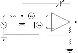
of an Electrometer Amplifier Used for Glass Micropipette Intracellular Recording
Measurement of the transmembrane potential of neurons, muscle cells, and other cells is generally done with hollow glass micropipettes filled with a conductive electrolyte solution such as 3M KCl (Lavallée et al., 1969). In order for the glass micropipette electrode to penetrate the cell membrane, the tips are drawn down to diameters of the order of 0.5 μm; the small diameter tips give micropipettes their high series resistance, Rμ. Figure 9.18 illustrates a simplified lumped-parameter model for a glass microelectrode with its tip in a cell. Rμ is on the order of 50 to 500 megohms. CT is the equivalent lumped shunt capacitance across the electrode’s tip glass; it is on the order of single picofarads.
The electrometer amplifier (EA) used to condition signals recorded intracellularly with a glass micropipette microelectrode is direct-coupled, has a low noninverting gain between 2 and 5, and is characterized by its extremely high input impedance (approximately 1015 Ω) and very low dc bias current (approximately 100 fA). The latter two properties are necessary because the
|
|
CN |
|
|
R @ T |
ena |
Vi |
|
|
V1 |
|
|||
+ |
|
EOA |
Vo |
|
Vb |
ina |
|||
Vi’ |
|
|||
C + Cin |
|
|
RF |
|
|
|
|
||
|
|
|
R1 |
FIGURE 9.18
Circuit used to model noise in a capacity-neutralized electrometer amplifier supplied by a glass micropipette electrode. Only white thermal noise from the microelectrode’s internal resistance is considered along with the white noises, ena and ina.
© 2004 by CRC Press LLC

364 |
Analysis and Application of Analog Electronic Circuits |
Thevenin source resistance of the microelectrode is so high and, for practical reasons, negligible dc bias current should flow through it to prevent ion drift at the tip. For all practical purposes, the EA can be treated as a noisy but otherwise ideal voltage amplifier. The so-called capacitive neutralization is accomplished by positive feedback applied though the variable capacitor, CN.
The transfer functions for the biosignal, Vb, and the amplifier noises, ena and ina, will now be found. Assume the EA’s gain is +3. To do this, first write the node equation for the v1 node in terms of the Laplace variable, s:
V1 [Gμ + sCT + sCN] − 3V1 sCN = Vb Gμ |
(9.96) |
Equation 9.96 can be solved for V1:
V1 |
= |
|
|
Vb |
|
(9.97) |
|
|
+ s Rμ (CT |
− 2CN ) |
|||
|
1 |
|
||||
Thus, |
|
|
|
|
|
|
Vo |
= |
|
|
3Vb |
|
(9.98) |
|
|
+ s Rμ (CT |
− 2CN ) |
|||
|
1 |
|
||||
Note that, in this simple case, when CN is made CT/2, the amplifier’s time constant 0, thus the break frequency fb = 1/2πτ • and Vo = 3Vb.
Now consider the transfer function for the EA’s current noise, ina:
V1 [Gμ + s (CT + CN)] − 3V1CN = ina
This node equation leads to the transfer impedance:
Vo |
= |
3 Rμ |
|
1+ s Rμ (CT − 2CN ) |
|
ina |
(9.99)
(9.100)
Now find the transfer function for ena. Again, write a node equation:
V1′[Gμ + s (CT + CN)] − 3V1CN = 0 |
(9.101) |
Note that when V1′ = V1 − ena is substituted into Equation 9.101, it is possible to solve for the transfer function:
V |
= |
3[1+ s Rμ (CT |
+ CN )] |
(9.102) |
|
o |
|
|
|||
ena |
1+ s Rμ (CT − 2CN ) |
||||
|
|
||||
In summary, when CN = CT/2, the amplifier is neutralized and the noise gains are:
© 2004 by CRC Press LLC