

- •Analysis and Application of Analog Electronic Circuits to Biomedical Instrumentation
- •Dedication
- •Preface
- •Reader Background
- •Rationale
- •Description of the Chapters
- •Features
- •The Author
- •Table of Contents
- •1.1 Introduction
- •1.2 Sources of Endogenous Bioelectric Signals
- •1.3 Nerve Action Potentials
- •1.4 Muscle Action Potentials
- •1.4.1 Introduction
- •1.4.2 The Origin of EMGs
- •1.5 The Electrocardiogram
- •1.5.1 Introduction
- •1.6 Other Biopotentials
- •1.6.1 Introduction
- •1.6.2 EEGs
- •1.6.3 Other Body Surface Potentials
- •1.7 Discussion
- •1.8 Electrical Properties of Bioelectrodes
- •1.9 Exogenous Bioelectric Signals
- •1.10 Chapter Summary
- •2.1 Introduction
- •2.2.1 Introduction
- •2.2.4 Schottky Diodes
- •2.3.1 Introduction
- •2.4.1 Introduction
- •2.5.1 Introduction
- •2.5.5 Broadbanding Strategies
- •2.6 Photons, Photodiodes, Photoconductors, LEDs, and Laser Diodes
- •2.6.1 Introduction
- •2.6.2 PIN Photodiodes
- •2.6.3 Avalanche Photodiodes
- •2.6.4 Signal Conditioning Circuits for Photodiodes
- •2.6.5 Photoconductors
- •2.6.6 LEDs
- •2.6.7 Laser Diodes
- •2.7 Chapter Summary
- •Home Problems
- •3.1 Introduction
- •3.2 DA Circuit Architecture
- •3.4 CM and DM Gain of Simple DA Stages at High Frequencies
- •3.4.1 Introduction
- •3.5 Input Resistance of Simple Transistor DAs
- •3.7 How Op Amps Can Be Used To Make DAs for Medical Applications
- •3.7.1 Introduction
- •3.8 Chapter Summary
- •Home Problems
- •4.1 Introduction
- •4.3 Some Effects of Negative Voltage Feedback
- •4.3.1 Reduction of Output Resistance
- •4.3.2 Reduction of Total Harmonic Distortion
- •4.3.4 Decrease in Gain Sensitivity
- •4.4 Effects of Negative Current Feedback
- •4.5 Positive Voltage Feedback
- •4.5.1 Introduction
- •4.6 Chapter Summary
- •Home Problems
- •5.1 Introduction
- •5.2.1 Introduction
- •5.2.2 Bode Plots
- •5.5.1 Introduction
- •5.5.3 The Wien Bridge Oscillator
- •5.6 Chapter Summary
- •Home Problems
- •6.1 Ideal Op Amps
- •6.1.1 Introduction
- •6.1.2 Properties of Ideal OP Amps
- •6.1.3 Some Examples of OP Amp Circuits Analyzed Using IOAs
- •6.2 Practical Op Amps
- •6.2.1 Introduction
- •6.2.2 Functional Categories of Real Op Amps
- •6.3.1 The GBWP of an Inverting Summer
- •6.4.3 Limitations of CFOAs
- •6.5 Voltage Comparators
- •6.5.1 Introduction
- •6.5.2. Applications of Voltage Comparators
- •6.5.3 Discussion
- •6.6 Some Applications of Op Amps in Biomedicine
- •6.6.1 Introduction
- •6.6.2 Analog Integrators and Differentiators
- •6.7 Chapter Summary
- •Home Problems
- •7.1 Introduction
- •7.2 Types of Analog Active Filters
- •7.2.1 Introduction
- •7.2.3 Biquad Active Filters
- •7.2.4 Generalized Impedance Converter AFs
- •7.3 Electronically Tunable AFs
- •7.3.1 Introduction
- •7.3.3 Use of Digitally Controlled Potentiometers To Tune a Sallen and Key LPF
- •7.5 Chapter Summary
- •7.5.1 Active Filters
- •7.5.2 Choice of AF Components
- •Home Problems
- •8.1 Introduction
- •8.2 Instrumentation Amps
- •8.3 Medical Isolation Amps
- •8.3.1 Introduction
- •8.3.3 A Prototype Magnetic IsoA
- •8.4.1 Introduction
- •8.6 Chapter Summary
- •9.1 Introduction
- •9.2 Descriptors of Random Noise in Biomedical Measurement Systems
- •9.2.1 Introduction
- •9.2.2 The Probability Density Function
- •9.2.3 The Power Density Spectrum
- •9.2.4 Sources of Random Noise in Signal Conditioning Systems
- •9.2.4.1 Noise from Resistors
- •9.2.4.3 Noise in JFETs
- •9.2.4.4 Noise in BJTs
- •9.3 Propagation of Noise through LTI Filters
- •9.4.2 Spot Noise Factor and Figure
- •9.5.1 Introduction
- •9.6.1 Introduction
- •9.7 Effect of Feedback on Noise
- •9.7.1 Introduction
- •9.8.1 Introduction
- •9.8.2 Calculation of the Minimum Resolvable AC Input Voltage to a Noisy Op Amp
- •9.8.5.1 Introduction
- •9.8.5.2 Bridge Sensitivity Calculations
- •9.8.7.1 Introduction
- •9.8.7.2 Analysis of SNR Improvement by Averaging
- •9.8.7.3 Discussion
- •9.10.1 Introduction
- •9.11 Chapter Summary
- •Home Problems
- •10.1 Introduction
- •10.2 Aliasing and the Sampling Theorem
- •10.2.1 Introduction
- •10.2.2 The Sampling Theorem
- •10.3 Digital-to-Analog Converters (DACs)
- •10.3.1 Introduction
- •10.3.2 DAC Designs
- •10.3.3 Static and Dynamic Characteristics of DACs
- •10.4 Hold Circuits
- •10.5 Analog-to-Digital Converters (ADCs)
- •10.5.1 Introduction
- •10.5.2 The Tracking (Servo) ADC
- •10.5.3 The Successive Approximation ADC
- •10.5.4 Integrating Converters
- •10.5.5 Flash Converters
- •10.6 Quantization Noise
- •10.7 Chapter Summary
- •Home Problems
- •11.1 Introduction
- •11.2 Modulation of a Sinusoidal Carrier Viewed in the Frequency Domain
- •11.3 Implementation of AM
- •11.3.1 Introduction
- •11.3.2 Some Amplitude Modulation Circuits
- •11.4 Generation of Phase and Frequency Modulation
- •11.4.1 Introduction
- •11.4.3 Integral Pulse Frequency Modulation as a Means of Frequency Modulation
- •11.5 Demodulation of Modulated Sinusoidal Carriers
- •11.5.1 Introduction
- •11.5.2 Detection of AM
- •11.5.3 Detection of FM Signals
- •11.5.4 Demodulation of DSBSCM Signals
- •11.6 Modulation and Demodulation of Digital Carriers
- •11.6.1 Introduction
- •11.6.2 Delta Modulation
- •11.7 Chapter Summary
- •Home Problems
- •12.1 Introduction
- •12.2.1 Introduction
- •12.2.2 The Analog Multiplier/LPF PSR
- •12.2.3 The Switched Op Amp PSR
- •12.2.4 The Chopper PSR
- •12.2.5 The Balanced Diode Bridge PSR
- •12.3 Phase Detectors
- •12.3.1 Introduction
- •12.3.2 The Analog Multiplier Phase Detector
- •12.3.3 Digital Phase Detectors
- •12.4 Voltage and Current-Controlled Oscillators
- •12.4.1 Introduction
- •12.4.2 An Analog VCO
- •12.4.3 Switched Integrating Capacitor VCOs
- •12.4.6 Summary
- •12.5 Phase-Locked Loops
- •12.5.1 Introduction
- •12.5.2 PLL Components
- •12.5.3 PLL Applications in Biomedicine
- •12.5.4 Discussion
- •12.6 True RMS Converters
- •12.6.1 Introduction
- •12.6.2 True RMS Circuits
- •12.7 IC Thermometers
- •12.7.1 Introduction
- •12.7.2 IC Temperature Transducers
- •12.8 Instrumentation Systems
- •12.8.1 Introduction
- •12.8.5 Respiratory Acoustic Impedance Measurement System
- •12.9 Chapter Summary
- •References

General Properties of Electronic Single-Loop Feedback Systems |
187 |
In practical cases, Kvo RF 3(RF + RL), so the VCCS’s transconductance can be approximated as:
GM (jω) |
|
|
GF |
|
jωτa 3 |
(RF |
+ RL ) (KvoRF )+ 1 |
||
|
Thus, it is clear that GM(0) GF and the break frequency is:
fb |
|
KvoRF |
|
|
2 πτa 3(RF + RL ) |
(4.61)
(4.62)
which is certainly greater than the op amp’s fT.
The VCCS’s Zout(jω) is now of interest. Ideally, it should approach infinity. To find it, take the ratio of the circuit’s OCV to SCC. Under OCV conditions, IL = 0 and VL = Vo. Using the node equation for Vi′, it is easy to write:
OCV = |
−VsKvo |
|
(4.63) |
||
3 jωτ |
|
+ |
1 |
||
|
( |
a |
|
) |
|
Next, find the VCCS’s SCC. Under SCC conditions, RL = 0 and VL = 0. The node equation for Vi′ yields:
|
R |
( |
K + 3 |
) |
jω3τ |
|
( |
K + 3 |
) |
+ 1 |
|
R K |
|
jω3τ |
|
K |
|
+ 1 |
|
|||||
|
F |
vo |
|
|
|
a |
|
vo |
] |
|
vo[ |
a |
vo |
|
||||||||||
Zout (jω) = |
|
[ |
|
|
|
|
|
|
|
F |
|
|
|
|
] |
(4.64) |
||||||||
|
|
|
( |
jωτ |
a |
|
|
) |
|
|
|
|
( |
jωτ |
a |
|
) |
|
||||||
|
|
|
|
3 |
|
|
+ 1 |
|
|
|
|
|
3 |
|
|
+ 1 |
|
|
|
|||||
From Equation 4.64 it can be seen that, at low frequencies, Zout(0) = RFKvo/3. At frequencies above Kvo/3τa r/s, Zout(hi) RF, which is not very high, making a poor VCCS at high frequencies.
4.5Positive Voltage Feedback
4.5.1Introduction
Positive voltage feedback (PVF) is seldom used in SISO feedback amplifiers. PVF increases the closed-loop gain, decreases the closed-loop bandwidth, increases the Rout of the system, and increases harmonic distortion at a given output level. These activities are based on the fact that the loop gain in a simple SISO feedback amplifier with PVF is AL = +βKv, so for +βKv < 1, the return difference, (1 – AL), is <1. PVF can be used deliberately to make a feed-back system unstable so that it oscillates. The next section illustrates
© 2004 by CRC Press LLC
188 |
Analysis and Application of Analog Electronic Circuits |
the use of PVF to increase the bandwidth of an amplifier used to couple intracellular glass micropipette electrodes used in neurophysiology to further signal conditioning stages.
4.5.2Amplifier with Capacitance Neutralization
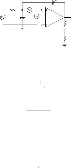
Glass micropipette electrodes (GMEs) are used to penetrate cell membranes, allowing the measurement of the dc resting potential across the membrane and, in the case of nerve and muscle cells, the transient action potentials associated with these cells. GMEs are made by heating and pulling smalldiameter, borosilicate class capillary tubing to a small diameter tip, which can range from 0.3 to 1 μm ID. The GMEs are then artfully filled with a conductive electrolyte solution such as 3 M KCl or potassium citrate, etc. A Ag AgCl fine wire electrode is inserted in the outer (large) end of the filled GME. By the arcane arts of electrophysiology, the GME tip is caused to penetrate a cell under investigation. The cell membrane generally forms a tight seal around the tip of the GME.
A stand-alone GME with its tip immersed in a beaker of saline in which a large reference electrode is also located allows one to measure the impedance of the filled GME. At dc and very low frequencies, the resistance of the GME can be on the order of 10 to 500 megohms, depending on the GME’s geometry and the filling electrolyte. There is also distributed stray capacitance between the tip lumen and the external electrolyte; the glass serves as the dielectric. Thus, the immersed tip appears as an RC transmission line giving distributed-parameter low-pass filtering to any time-varying potential seen at the tip (Webster, 1992, Chapter 5; Lavallée et al., 1969).
Rather than deal with the complexity of a transmission-line low-pass filter and include the ac characteristics of the AgCl coupling and reference electrodes, the GME will be oversimplified in situ by a simple RC low-pass filter; Rμ is the GME’s total DC resistance and Cμ represents the total effective shunting capacitance of the GME’s tip. Figure 4.7 shows the GME attached to the PVF amplifier, which uses an electrometer op amp that has a dc input bias current on the order of tens of femptoamps. It is thus characterized by an input resistance on the order of 1013 Ω and an input capacitance to ground, Cin, on the order of single pF. The PVF is applied through a variable capacitor, CN. The noninverting gain of the amplifier, Avo, is on the order 2 to 5 and is set by resistors RF and R1.
To begin the analysis of this PVF amplifier, consider the gain between the noninverting node and the output, Vo/Vi. This gain is found by writing the node equation for the Vi′ node:
Vi′[GF |
+ G1] − Vo GF = 0 |
(4.65) |
|||||
and |
|
|
|
|
|
|
|
V = |
( |
V − V′ |
Kvo |
|
(4.66) |
||
|
|
+ 1 |
|||||
o |
i i ) jωτ |
a |
|
||||
|
|
|
|
|
|
|
|
© 2004 by CRC Press LLC
General Properties of Electronic Single-Loop Feedback Systems |
189 |
|||
|
|
|
CN |
|
|
R @ T V1 |
ena |
Vi |
|
|
|
|
||
+ |
|
|
|
Vo |
|
|
ina |
|
|
Vb |
C + Cin |
EOA |
|
|
|
|
|||
RF
Vi’
R1
FIGURE 4.7
Schematic of a noninverting electrometer op amp with positive voltage feedback through a small neutralizing capacitor, CN. This circuit is used with glass micropipette microelectrodes to increase system bandwidth.
Substituting Equation 4.66 into Equation 4.65 and assuming R1Kvo/(R1 + RF) 1 reveals the frequency response function:
Vo |
= |
(1+ RF |
R1) |
(4.67) |
|
jωτa (1+ RF |
R1) Kvo + 1 |
||
Vi |
Next, examine the simple low-pass frequency response function of the GME alone:
Vi |
1 |
|
|
|
= |
jωRμ (Cμ + Cin )+ 1 |
(4.68) |
Vb |
|||
To find the frequency response of the amplifier with PVF through CN, write the node equation for Vi:
Vi [Gμ + jω(CT + CN)] − Vo jωCN = Vb Gμ |
(4.69) |
||||||||
Note that: |
|
|
|
|
|
|
|
||
|
|
CT = Cμ + Cin |
|
|
(4.70) |
||||
and |
|
|
|
|
|
|
|
||
|
Vo |
= |
|
|
Avo |
|
|
|
(4.71) |
|
|
jωτ |
|
A K |
|
+ 1 |
|||
|
V |
a |
vo |
|
|||||
|
i |
|
vo |
|
|
|
|||
where Avo ∫ (1 + RF/R1). Substituting from the preceding equations, the node equation can be written:
© 2004 by CRC Press LLC