

- •Analysis and Application of Analog Electronic Circuits to Biomedical Instrumentation
- •Dedication
- •Preface
- •Reader Background
- •Rationale
- •Description of the Chapters
- •Features
- •The Author
- •Table of Contents
- •1.1 Introduction
- •1.2 Sources of Endogenous Bioelectric Signals
- •1.3 Nerve Action Potentials
- •1.4 Muscle Action Potentials
- •1.4.1 Introduction
- •1.4.2 The Origin of EMGs
- •1.5 The Electrocardiogram
- •1.5.1 Introduction
- •1.6 Other Biopotentials
- •1.6.1 Introduction
- •1.6.2 EEGs
- •1.6.3 Other Body Surface Potentials
- •1.7 Discussion
- •1.8 Electrical Properties of Bioelectrodes
- •1.9 Exogenous Bioelectric Signals
- •1.10 Chapter Summary
- •2.1 Introduction
- •2.2.1 Introduction
- •2.2.4 Schottky Diodes
- •2.3.1 Introduction
- •2.4.1 Introduction
- •2.5.1 Introduction
- •2.5.5 Broadbanding Strategies
- •2.6 Photons, Photodiodes, Photoconductors, LEDs, and Laser Diodes
- •2.6.1 Introduction
- •2.6.2 PIN Photodiodes
- •2.6.3 Avalanche Photodiodes
- •2.6.4 Signal Conditioning Circuits for Photodiodes
- •2.6.5 Photoconductors
- •2.6.6 LEDs
- •2.6.7 Laser Diodes
- •2.7 Chapter Summary
- •Home Problems
- •3.1 Introduction
- •3.2 DA Circuit Architecture
- •3.4 CM and DM Gain of Simple DA Stages at High Frequencies
- •3.4.1 Introduction
- •3.5 Input Resistance of Simple Transistor DAs
- •3.7 How Op Amps Can Be Used To Make DAs for Medical Applications
- •3.7.1 Introduction
- •3.8 Chapter Summary
- •Home Problems
- •4.1 Introduction
- •4.3 Some Effects of Negative Voltage Feedback
- •4.3.1 Reduction of Output Resistance
- •4.3.2 Reduction of Total Harmonic Distortion
- •4.3.4 Decrease in Gain Sensitivity
- •4.4 Effects of Negative Current Feedback
- •4.5 Positive Voltage Feedback
- •4.5.1 Introduction
- •4.6 Chapter Summary
- •Home Problems
- •5.1 Introduction
- •5.2.1 Introduction
- •5.2.2 Bode Plots
- •5.5.1 Introduction
- •5.5.3 The Wien Bridge Oscillator
- •5.6 Chapter Summary
- •Home Problems
- •6.1 Ideal Op Amps
- •6.1.1 Introduction
- •6.1.2 Properties of Ideal OP Amps
- •6.1.3 Some Examples of OP Amp Circuits Analyzed Using IOAs
- •6.2 Practical Op Amps
- •6.2.1 Introduction
- •6.2.2 Functional Categories of Real Op Amps
- •6.3.1 The GBWP of an Inverting Summer
- •6.4.3 Limitations of CFOAs
- •6.5 Voltage Comparators
- •6.5.1 Introduction
- •6.5.2. Applications of Voltage Comparators
- •6.5.3 Discussion
- •6.6 Some Applications of Op Amps in Biomedicine
- •6.6.1 Introduction
- •6.6.2 Analog Integrators and Differentiators
- •6.7 Chapter Summary
- •Home Problems
- •7.1 Introduction
- •7.2 Types of Analog Active Filters
- •7.2.1 Introduction
- •7.2.3 Biquad Active Filters
- •7.2.4 Generalized Impedance Converter AFs
- •7.3 Electronically Tunable AFs
- •7.3.1 Introduction
- •7.3.3 Use of Digitally Controlled Potentiometers To Tune a Sallen and Key LPF
- •7.5 Chapter Summary
- •7.5.1 Active Filters
- •7.5.2 Choice of AF Components
- •Home Problems
- •8.1 Introduction
- •8.2 Instrumentation Amps
- •8.3 Medical Isolation Amps
- •8.3.1 Introduction
- •8.3.3 A Prototype Magnetic IsoA
- •8.4.1 Introduction
- •8.6 Chapter Summary
- •9.1 Introduction
- •9.2 Descriptors of Random Noise in Biomedical Measurement Systems
- •9.2.1 Introduction
- •9.2.2 The Probability Density Function
- •9.2.3 The Power Density Spectrum
- •9.2.4 Sources of Random Noise in Signal Conditioning Systems
- •9.2.4.1 Noise from Resistors
- •9.2.4.3 Noise in JFETs
- •9.2.4.4 Noise in BJTs
- •9.3 Propagation of Noise through LTI Filters
- •9.4.2 Spot Noise Factor and Figure
- •9.5.1 Introduction
- •9.6.1 Introduction
- •9.7 Effect of Feedback on Noise
- •9.7.1 Introduction
- •9.8.1 Introduction
- •9.8.2 Calculation of the Minimum Resolvable AC Input Voltage to a Noisy Op Amp
- •9.8.5.1 Introduction
- •9.8.5.2 Bridge Sensitivity Calculations
- •9.8.7.1 Introduction
- •9.8.7.2 Analysis of SNR Improvement by Averaging
- •9.8.7.3 Discussion
- •9.10.1 Introduction
- •9.11 Chapter Summary
- •Home Problems
- •10.1 Introduction
- •10.2 Aliasing and the Sampling Theorem
- •10.2.1 Introduction
- •10.2.2 The Sampling Theorem
- •10.3 Digital-to-Analog Converters (DACs)
- •10.3.1 Introduction
- •10.3.2 DAC Designs
- •10.3.3 Static and Dynamic Characteristics of DACs
- •10.4 Hold Circuits
- •10.5 Analog-to-Digital Converters (ADCs)
- •10.5.1 Introduction
- •10.5.2 The Tracking (Servo) ADC
- •10.5.3 The Successive Approximation ADC
- •10.5.4 Integrating Converters
- •10.5.5 Flash Converters
- •10.6 Quantization Noise
- •10.7 Chapter Summary
- •Home Problems
- •11.1 Introduction
- •11.2 Modulation of a Sinusoidal Carrier Viewed in the Frequency Domain
- •11.3 Implementation of AM
- •11.3.1 Introduction
- •11.3.2 Some Amplitude Modulation Circuits
- •11.4 Generation of Phase and Frequency Modulation
- •11.4.1 Introduction
- •11.4.3 Integral Pulse Frequency Modulation as a Means of Frequency Modulation
- •11.5 Demodulation of Modulated Sinusoidal Carriers
- •11.5.1 Introduction
- •11.5.2 Detection of AM
- •11.5.3 Detection of FM Signals
- •11.5.4 Demodulation of DSBSCM Signals
- •11.6 Modulation and Demodulation of Digital Carriers
- •11.6.1 Introduction
- •11.6.2 Delta Modulation
- •11.7 Chapter Summary
- •Home Problems
- •12.1 Introduction
- •12.2.1 Introduction
- •12.2.2 The Analog Multiplier/LPF PSR
- •12.2.3 The Switched Op Amp PSR
- •12.2.4 The Chopper PSR
- •12.2.5 The Balanced Diode Bridge PSR
- •12.3 Phase Detectors
- •12.3.1 Introduction
- •12.3.2 The Analog Multiplier Phase Detector
- •12.3.3 Digital Phase Detectors
- •12.4 Voltage and Current-Controlled Oscillators
- •12.4.1 Introduction
- •12.4.2 An Analog VCO
- •12.4.3 Switched Integrating Capacitor VCOs
- •12.4.6 Summary
- •12.5 Phase-Locked Loops
- •12.5.1 Introduction
- •12.5.2 PLL Components
- •12.5.3 PLL Applications in Biomedicine
- •12.5.4 Discussion
- •12.6 True RMS Converters
- •12.6.1 Introduction
- •12.6.2 True RMS Circuits
- •12.7 IC Thermometers
- •12.7.1 Introduction
- •12.7.2 IC Temperature Transducers
- •12.8 Instrumentation Systems
- •12.8.1 Introduction
- •12.8.5 Respiratory Acoustic Impedance Measurement System
- •12.9 Chapter Summary
- •References
Analog Active Filters |
|
|
|
297 |
|
R |
|
V1 |
|
|
|
I1 |
|
|
|
|
Z1 |
R |
|
|
|
|
|
|
VS |
|
|
|
|
|
|
|
V2 |
IOA |
|
|
|
|
|
|
|
Z2 |
R |
|
|
|
|
|
|
|
|
(V1) |
|
|
|
|
Z3 |
C |
|
|
|
|
|
|
Vo = V2 |
|
V3 |
|
|
|
IOA |
|
||
|
|
|
|
|
|
|
Z4 |
R |
|
|
C |
|
|
|
|
|
|
(V1) |
|
|
|
Z5 |
R |
|
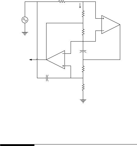
FIGURE 7.12
A GIC all-pass filter.
In summary, note again that the major reason for using the GIC architecture is to realize AFs that are useful at very low frequencies, e.g., 0.01 to 10 Hz, without having to use expensive, very large capacitances.
7.3Electronically Tunable AFs
7.3.1Introduction
In many biomedical instrumentation systems, a conditioned (by filtering) analog signal is periodically sampled and digitized. The digital number sequence is then further processed by certain digital algorithms that can include, but are not limited to: signal averaging; computation of signal statistics (e.g., mean, RMS value, etc.); computation of the discrete Fourier transform; convolution with another signal or kernel; etc. The computer is often used to change the input filter’s parameters (half-power frequencies or center frequency; damping factor or Q) to accommodate a new sampling rate or changes in the analog signal’s power spectrum.
A particular application of a computer-controlled analog filter is the antialiasing (A-A) low-pass filter. In order to prevent aliasing and the problems
© 2004 by CRC Press LLC
298 |
|
Analysis and Application of Analog Electronic Circuits |
|||
|
|
R |
|
V1 |
|
|
|
|
I1 |
|
|
|
|
|
Z1 |
R |
|
|
|
|
|
|
|
|
VS |
|
|
|
|
|
|
|
|
V2 |
IOA |
|
|
|
|
|
|
|
|
|
Z2 |
R |
|
|
|
|
|
|
|
|
|
|
(V1) |
|
|
|
|
|
Z3 |
C |
|
|
|
|
|
|
|
|
Vo = V2 |
|
V3 |
|
|
|
|
IOA |
|
||
|
|
|
|
|
|
|
|
|
Z4 |
R |
|
|
|
C |
|
|
|
|
|
|
|
(V1) |
|
|
|
R |
|
|
|
|
|
|
Z5 |
R |
|
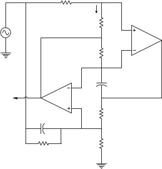
FIGURE 7.13
A GIC notch filter.
this creates for the signal in digital form, the A-A filter must pass no significant signal spectral power to the analog-to-digital converter at frequencies above one half the sampling frequency, fs. fs/2 is called the Nyquist frequency, fn. (See Section 10.2 in Chapter 10 for a complete treatment of sampling and aliasing.)
The key to designing a digitally tuned filter is the variable gain element (VGE) (Northrop, 1990, Section 10.1). The design of digitally-controlled variable gain elements (DCVGEs) has several approaches: one uses a digital-to- analog converter (DAC) configured to produce 0 to 10 Vdc output, VC, which is the input to an analog multiplier IC; the other input to the analog multiplier is the time-variable analog signal, vk (t), whose amplitude is to be adjusted. The output of the analog multiplier is then vk′(t) = vk (t)VC/10. VC/10 varies from 0 to 1 in steps determined by the quantization set by the number of binary bits input to the DAC. Another VGE is the digitally programmed gain amplifier (DPGA), with a gain digitally selected in 6-dB steps (i.e., 1, 2, 4, 8, 16, 32, 64, and 128) using a 3-bit input word (e.g., the MN2020). Still another class of DCVGE is represented by the AD8400, 8-bit, digitally controlled potentiometer (DCP) connected as a variable resistor. The DCP resistance is given by:
N |
|
Vj′ = Rtotal Bk 2k−(1+N ) = Rtotal Ak |
(7.55) |
k=1
© 2004 by CRC Press LLC
Analog Active Filters |
299 |
R |
|
R |
|
V2 R/(2ξ) |
R |
2ξR |
C |
VS |
V3 DPA V3’ R |
IOA |
|
R |
IOA |
IOA V4
WN
C
R V4’
V5 = Vo
IOA
DPA
N
η = V3’/V3 = V4’/V4 = ( Σ Bk 2k −1)/2N
k = 1
k = 1 is LSB, k = 8 is MSB. WN = {Bk}
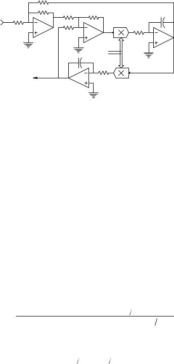
FIGURE 7.14
The use of two parallel digitally controlled attenuators to tune the break frequency of a twoloop biquad low-pass filter at constant damping. See text for analysis.
where N is the number of bits controlling the DCP and Bk is the kth bit state (0 or 1). Note that the DCP is similar in operation to a 2-quadrant multiplying digital-to-analog converter (MDAC), which also can be used as a DCVGE (Northrop, 1990).
The following sections examine how DCVGEs can tune a two-loop biquad A-A LPF’s ωn and Q.
7.3.2The Tunable Two-Loop Biquad LPF
Figure 7.14 illustrates the schematic of a 2-loop biquad LPF with digital control of its natural frequency at constant damping using 8-bit digitally controlled attenuators (DCAs). (One form of a DCA that uses DPP is shown in Figure 7.15.) It is easy to derive this digitally tuned LPF’s transfer function using Mason’s rule:
Vo |
(s) = |
|
(−1 2ξ)(−2ξ)(η)(−1 sRC)(η)(−1 sRC) |
|
|||
|
1− [(−1)(−2ξ)(η)(−1 sRC)+ (−1)(η)(−1 sRC)(η)(−1 sRC)] |
(7.56A) |
|||||
VS |
|||||||
|
|
|
|
¬ |
|
|
|
|
|
|
Vo |
1 |
|
|
|
|
|
|
|
(s) = |
|
|
(7.56B) |
|
|
|
VS |
s2 (RC η)2 + s(RC η)(2ξ) + 1 |
|||
© 2004 by CRC Press LLC
300 |
Analysis and Application of Analog Electronic Circuits |
|
|
|
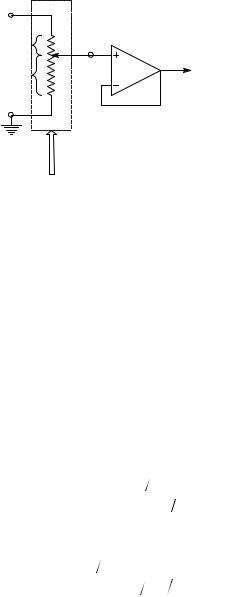
A DCA |
|
|
DCP |
|
Vin |
|
|
|
Buffer |
|
(1 − η) Rtotal |
ηVin |
Vo = ηVin
η Rtotal IOA
WN
FIGURE 7.15
Schematic of a digitally controlled attenuator (DCA).
From the standard quadratic format:
ωn = η/RC r/s |
(7.57) |
The constant damping, ξ, is set by the size of the input resistor (2 ξR) and the resistor size V2 sees (R/2 ξ). Thus, with 1 LSB in, Wn = {0,0,0,0,0,0,0,1}, ωn = (1/256)(1/RC) r/s; with WN = {1,1,1,1,1,1,1,1}, ωn = (255/256)(1/RC) r/s. The dc gain of the filter is +1.
As a second example, consider the digitally controlled band-pass filter shown in Figure 7.16 in which two N-bit, serial binary words (WN1 and WN2) are used to set the filter’s natural frequency, ωn, and a third variable gain element is used to adjust the filter’s Q. In this example, digitally controlled amplifier gains are used. Using Mason’s rule as before, the transfer function can be written as:
V4 |
(s) = |
|
|
|
|
|
|
(−1)A1(−1 128)A2 (−1 sRC) |
|
|
|
(7.58) |
|||||||||
V |
1− |
−1 |
A |
1 |
( |
−1 |
128 A |
( |
−1 sRC |
) |
+ |
−1 |
A |
2 |
( |
−1 sRC A |
2 ( |
−1 sRC |
)] |
||
S |
|
|
[( ) |
|
|
) 2 |
|
|
( ) |
|
) |
|
|
||||||||
¬
V |
(s) = |
−s(A1 A2 )RC 128 |
|
4 |
|
|
|
VS |
s2 (RC A2 )2 + sRC(A1 A2 ) 128 + 1 |
|
|
where the resonant frequency is set by A2 and the Q by 1/A1: ωn = A2/RC r/s
Q = 128/A1
(7.59)
(7.60A)
(7.60B)
© 2004 by CRC Press LLC