


162 |
|
Analysis and Application of Analog Electronic Circuits |
|
|
−Vs’ |
IOA |
3’ |
|
|
||
|
V2’ |
|
R4’ |
|
|
R2’ |
|
|
|
R1’ |
R3’ |
|
|
|
|
|
|
|
Vo |
|
|
Vc |
IOA |
|
|
|
R3 |
|
|
R1 |
(DA) |
|
|
|
|
|
|
R2 |
R4 |
|
V2 |
|
|
|
+Vs |
IOA |
3 |
|
|
|
|
FIGURE 3.16
The symmetrical three-op amp DA. Again, for max CMRR, the primed resistors must precisely equal the corresponding nonprimed resistors.
Clearly, for CM signals:
A = |
Vo |
= 0 |
(3.41) |
|
|||
C |
Vsc |
|
|
|
|
|
For pure DM excitation, Vs′ = −Vs, V2 = Vs = Vsd, and V2′ = −Vs. Thus a potential of 2Vs exists across resistors (R1 + R1′ ) and, by Kirchoff’s voltage
law, Vc = 0 on the axis of symmetry.
Because current flows through R1 and R2, and also R1′ and R2′, the input
IOAs each have a gain of (1 + R2/R1). Now V3′ = −Vsd (1 + R2/R1) and V3 = Vsd (1 + R2/R1). Using superposition on the output IOA circuit yields:
Vo |
= AD = (R4 R3 )2(1+ R2 R1) |
(3.42) |
|
||
Vsd |
|
|
IC versions of this DA circuit generally make R3 = R4, set the R2s = 25 k, and replace (R1 + R1′ ) with a single external resistor to set AD between 1 and 103. An example of such an IC DA is the Burr–Brown INA111. In practice, the OAs are not ideal and have different, finite CMRRs, and the resistors are not perfectly matched. For example, the “off-the-shelf” CMRR is 106 dB at an AD = 100 for the INA111.
3.8Chapter Summary
Because of their great importance in many aspects of analog electronic circuit design, differential amplifiers have been treated in their own chapter. DAs
© 2004 by CRC Press LLC
The Differential Amplifier |
163 |
are essential electronic subsystems for ICs such as op amps, instrumentation amplifiers, and analog voltage comparators. DAs are widely used in instrumentation systems to condition signals because of their ability to reject, by subtraction, interference and noise that are exactly common to both inputs.
In describing DA circuit architecture, important definitions of differential and common-mode input signals, differential and common-mode gains, and common-mode rejection ratio (CMRR) as a DA figure of merit were introduced. Internal and external factors affecting the DA’s CMRR at low frequencies were described.
The midand high-frequency behavior of DA difference-mode and commonmode gains were explored by circuit simulation and factors affecting the CMRR at high frequencies were discussed. Circuits using twoand three-op amps to make instrumentation DAs were described and analyzed.
Home Problems
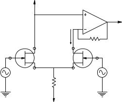
3.1A pair of matched JFETs and an ideal op amp are used to make a DA as shown in Figure P3.1. Both JFETs are described at mid-frequencies by the simple Norton (gm, gd) MFSSM.
a.Draw the complete MFSSM for the DA. Note that the MFSSM treats all dc voltage sources as small signal grounds and all dc current sources as open circuits.
b.Use superposition to derive an expression for vo = f(v1, v2). Show what happens to vo when RS is replaced with an ideal dc current source.
VDD
IOA |
vo |
id2
RF
D
vs
v1 |
S |
S |
v2 |
RS
−VSS
FIGURE P3.1
© 2004 by CRC Press LLC
164 |
Analysis and Application of Analog Electronic Circuits |
VCC
RB |
RC |
RC |
|
RB |
Q1 |
vo |
vo’ |
Q2 |
|
• |
|
|
|
• |
|
ve |
ve’ |
|
|
|
D |
D |
|
|
|
|
vs |
|
|
Q3 |
S |
S |
Q4 |
v1’ |
v1 |
|
RS
−VSS
FIGURE P3.2
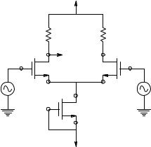
3.2The schematic of a JFET/BJT cascode DA is shown in Figure P3.2. In this
DA, Q1 = Q2 with hoe = hre = 0, hfe = 120, ICQ = 1 mA, RC = 7 kΩ, Rs = 25 MΩ (dynamic load), and RB = 1.24 MΩ. Also, Q3 = Q4 with gm = 5 ∞ 10−3 S, gd = 1 ∞ 10−4 S.
a.Use the bisection theorem to draw the MFSSMs for pure CM and pure DM excitation.
b.Find an expression for the CM gain, vo/v1c.
c.Find an expression for the DA’s DM gain, vo/v1d.
d.Find an expression for and evaluate numerically the DA’s CMRR.
3.3Figure P3.3A shows the schematic of a 2N2369 DA given DM excitation. VINV is an ideal VCVS with a gain of −1. The common emitters use an active
current sink that can be replaced by its Norton equivalent of a 2.0125-mA current source in parallel with a 2-MΩ resistor and a small shunt capacitance to ground, CE.
a.Use an ECAP to make a Bode plot of the DM gain, Vo/V1d, vs. f from 10 kHz to 10 GHz. Give values for the mid-frequency gain, the upper −3-dB frequency, and fT.
b.Figure P3.3B illustrates the DA given pure CM excitation. Now
the capacitor, CE, will affect the CM high frequency response.
Make a Bode plot of the CM gain, Vo/V1c over 1 kHz to 1 GHz with CE ∫ 0.
© 2004 by CRC Press LLC

The Differential Amplifier |
165 |
|
VINV |
|
|
A |
∞ −1 |
|
|
|
|
+15 V |
|
1.5 MΩ |
10 kΩ |
10 kΩ |
1.5 MΩ |
|
|
vo |
|
10 μF |
|
|
10 μF |
|
|
ve |
−v1 |
|
|
|
|
v1 |
2N2369 |
|
2N2369 |
|
|
CE |
|
|
2.0125 mA |
2 MΩ |
|
|
|
−15 V |
|
B |
|
+15 V |
|
|
|
|
|
1.5 MΩ |
10 kΩ |
10 kΩ |
1.5 MΩ |
|
|
vo |
|
10 μF |
|
|
10 μF |
|
|
|
v1 |
|
|
ve |
|
v1 |
2N2369 |
|
2N2369 |
|
|
CE |
|
|
2.0125 mA |
2 MΩ |
|
|
|
−15 V |
|
FIGURE P3.3
c.Now find a CE value by trial and error that will minimize the CM frequency response. (Hint: the optimum value lies between 1 and 10 pF.)
d.The decibel CMRR for the DA is just the decibel DM gain minus
the CM gain. Plot the decibel CMRR for the amplifier with CE = 0, and CE = the optimum value, for 10 kHz ≤ f ≤ 1 GHz.
©2004 by CRC Press LLC
166 |
Analysis and Application of Analog Electronic Circuits |
VDD
|
RD |
RD |
|
|
Q1 |
|
Q2 |
|
|
vo |
|
|
|
vs |
|
v1 |
S |
S |
v1’ |
|
|
D |
|
Q3 S
−VSS
FIGURE P3.4
3.4A MOSFET DA is shown in Figure P3.4.
a.Draw the complete MFSSM for the DA. Use the Norton model (gm, gd) for the MOSFETs.
b.Draw the left-hand MFSSM of the DA valid for DM inputs. Derive an expression for the MF Ad = vo/v1d.
c.Draw the left-hand MFSSM of the DA valid for CM inputs. Derive an expression for Ac = vo/v1c.
d.Give an expression for the CMRR of the DA.
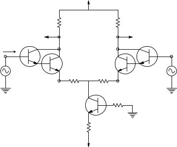
3.5Figure P3.5 illustrates a p-channel JFET DA with a pnp BJT dynamic source
load. Assume Q1 = Q2 with gm = 0.002 S, and rd = 250 kΩ. For the BJT: hfe = 150; hoe = 10−6 S; hie = 1.5 kΩ; and hre = 0.
a.Draw the MFSSM for the DA.
b.Find an expression and the numerical value for the SS resistance, RS, looking into the collector of the BJT.
c.Find the expression and numerical value for Ad = vo/v1d, Ac = vo/v1c, and the DA’s CMRR.
3.6The DA shown in Figure P5.6 uses common-mode negative feedback between
the output and the dynamic load BJT, Q3. Assume Q1 = Q2 with hfe = 200; hie = 2.5 kΩ; hoe = hre = 0; R1 = 70 kΩ; and RC = 4 kΩ. For Q3: hfe = 200; hoe = 10–5 S; hie = 1.2 kΩ; and hre = 0. The numbers in parentheses are quiescent dc bias voltages. The zener diode drops 14.3 V at 0.2 mA. Treat it as an ideal DC voltage source.
© 2004 by CRC Press LLC

The Differential Amplifier |
167 |
VDD = −15 V
3.5 kΩ |
RD |
RD 3.5 kΩ |
|
Q1 |
vo |
vo’ |
Q2 |
v1 |
S |
S |
v1’ |
|
Q3 |
RB |
|
|
|
2 kΩ |
|
|
3.5 kΩ |
RE |
|
VEE = +15 V
FIGURE P3.5
a.Use the bisection theorem to draw the MFSSM for the DA given pure DM excitation.
b.Use the bisection theorem to draw the MFSSM for the DA given pure CM excitation.
c.Give algebraic expressions for Ad = vo/v1d and Ac = vo/v1c. Evaluate numerically.
d.Evaluate the DA’s CMRR.
e.By way of comparison, repeat parts a through d when the zener diode is removed and Q3’s base is tied to small-signal ground.
3.7The DA shown in Figure P3.7 uses feedback pair amplifiers. For symmetry, Q1 = Q3 and Q2 = Q4, but Q1 π Q2, etc. Q1 and Q3 have hfe1, hie1 > 0, and hre1 = hoe1 = 0. Likewise, Q2 and Q4 have hfe2, hie2 > 0, and hre2 = hoe2 = 0.
a.Draw the complete MFSSM for the DA given pure DM excitation.
b.Draw the complete MFSSM for the DA given pure CM excitation.
c.Find an expression for Ad = vo/v1d.
d.Find an expression for Ac = vo/v1c.
e.Find an expression for the DA’s CMRR.
f.Find an expression for the DA’s small-signal input resistance when it is given DM input. Let Rind = v1d/i1.
g.Find an expression for the DA’s small-signal input resistance when it is given CM input. Let Rinc = v1c/i1.
© 2004 by CRC Press LLC

168 |
Analysis and Application of Analog Electronic Circuits |
|
+ 15 V |
|
RC |
RC |
(+7 V) |
R1 (0 V) R1 |
(+7 V) |
vo |
|
|
Q1 |
|
Q2 |
(0 V) |
|
(0 V) |
v1 |
(−0.7 V) |
v1’ |
|
||
Q3 |
|
|
|
(−14.3 V) |
|
− 15 V |
|
|
FIGURE P3.6
+VEE
|
R1 |
|
R1 |
|
vo |
|
vo’ |
i1 |
Q2 |
|
Q4 |
|
|
||
v1 |
Q1 |
R2 v3 R2 |
Q3 |
|
|
v1’ |
R3
−VCC
FIGURE P3.7
3.8Figure P3.8 illustrates a DA using Darlington modules, the purpose of which is to raise the DM input resistance. For symmetry, Q1 = Q3 and Q2 = Q4. Q1 and Q3 have hfe1, hie1 > 0, and hre1 = hoe1 = 0. Q2 and Q4 have hfe2, hie2 > 0, and hre2 = hoe2 = 0. Q5 has hfe5, hie5, and hoe5 > 0, hre5 = 0.
a.Draw the MFSSMs for the DA for pure CM and DM excitations.
b.Find an expression for Ad = vo/v1d.
© 2004 by CRC Press LLC
The Differential Amplifier |
169 |
VCC
RC |
RC |
vo |
vo’ |
Q1 |
Q3 |
i1 |
|
Q2 |
Q4 |
v1 |
v1’ |
RE ve |
RE |
Q5 |
RB |
|
RE3
−VEE
FIGURE P3.8
c.Find an expression for Ac = vo/v1c.
d.Find an expression for the DA’s CMRR.
e.Find an expression for the DA’s small-signal input resistance when it is given DM input. Let Rind = v1d/i1.
f.Find an expression for the DA’s small-signal input resistance when it is given CM input. Let Rinc = v1c/i1.
g.Now let hfe1 = 100, hie1 = 6 kΩ, hfe2 = 50, hie2 = 1 kΩ, hfe5 = 100, hoe5 = 10−5 S, hie5 = 2.5 kΩ, RC = 5 kΩ, RE = 500 Ω, RE3 = 3.3 kΩ, and RB = 100 kΩ. Calculate numerical values for parts b through f.
3.9Two, matched, n-channel JFETs are connected as shown in Figure P3.9. They
are both characterized by the saturation-region, JFET drain current relation: ID = IDSS (1 − VGS/VP)2. The capacitor, Co, blocks dc from the output signal. The circuit input is the pure difference-mode signal, vgd = v1. Find an algebraic expression for IL and the ac, vo.
3.10Two matched 2N2222A BJTs are used to make a BJT DA shown in Figure P3.10.
a.Simulate the circuit under CM excitation and make a Bode plot of Ac = Vo/V1c. Let 1k Hz ≤ f ≤ 0.1 GHz.
b.Now make a Bode plot of the DM gain, Ad = Vo/V1d.
c.Plot the DA’s CMRR in decibels over 1 kHz to 0.1 GHz.
©2004 by CRC Press LLC

170 |
Analysis and Application of Analog Electronic Circuits |
VDD
|
IL |
RD |
|
|
|
|
Co |
|
|
|
vo |
|
D |
D |
vg’ |
|
vg |
|
|
+ |
|
|
− |
|
|
|
|
v1 |
S |
|
v1 |
− |
|
VGSQ |
+ |
|
|
|
FIGURE P3.9
15 V
1.5 MΩ |
6 kΩ |
6 kΩ |
1.5 MΩ |
|
vo |
vo’ |
Q2 |
|
Q1 |
|
v1  v1’
v1’
1 µF |
µF |
|
ve |
Q1 = Q2 = 2N2222A
5 kΩ
−15 V
FIGURE P3.10
3.11A BJT DA is shown in Figure P3.11. The circuit is symmetrical. RE = 105 Ω, RS = 500 Ω, RC = 6.8 kΩ, RB = 1 MΩ; BJTs: hoe = hre = 0; hfe = 100; hie = 2.5 kΩ. Assume Cc is a small-signal short circuit.
a.Use MFSS analysis and the bisection theorem to find numerical values for AD, AC, and the CMRR. AD ∫ vo/v1d and AC ∫ vo/v1c.
b.Now the vo output is coupled to a 10-kΩ load resistance, RL, making the DA circuit asymmetrical, so the bisection theorem no longer can be used. Repeat a.
3.12It is desired to measure the CMRR of a student-built differential amplifier (see Figure P3.12). First, the two inputs are shorted together and connected to a
© 2004 by CRC Press LLC

The Differential Amplifier
RB
RS
Cc
vs
FIGURE P3.11
v1
IA
v1’
v1c
171
VCC
RC |
RC |
RB |
vo |
vo’ |
|
|
|
RS |
|
ve |
Cc |
|
|
|
|
|
vs’ |
|
RE |
|
−VE
v1
vo |
vo |
IA
vs v1’
FIGURE P3.12
100-Hz sinusoidal source. The source amplitude is adjusted so that when the peak output signal is 1.0 V, the input is 10 V, peak. Then the negative input to the amplifier is grounded and the source is connected to the + input. Its amplitude is adjusted so that Vo = 10 V, peak, when the input is 20 mV, peak. Find numerical values for AD, AC, and the CMRR in decibels.
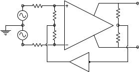
3.13Common-mode negative feedback is applied around a DA having a
differential output, shown in Figure P3.13. The amplifier follows the relations:
Vo = ADV1d + ACV1c; Vo′ = −ADV1d + ACV1c. Also, V1c = AC V1c, and let α ∫ R1/(R1 + Rs) and β = Rs/(R1 + Rs).
a.Use superposition to find expressions for V1 and V1′.
b.Find an expression for V1c when Vs and Vs′ are such that the input is pure Vsc.
© 2004 by CRC Press LLC
172 |
Analysis and Application of Analog Electronic Circuits |
||
|
Rs |
V1 |
Vo |
|
Vs |
R1 |
R |
|
|
||
|
|
DA |
Vo |
|
Vs’ |
R1 |
R |
|
|
|
|
|
Rs |
V1’ |
Vo’ |
|
|
||
|
KcmVoc |
Kcm |
|
FIGURE P3.13
c.Find an expression for V1d when the input is pure Vsd.
d.Find an expression for the CMNF amplifier’s CMRR. Compare it to the CMRR of the DA alone. Let R1 = R2 = 106 Ω; Kcm = −103; AC = 1, and AD = 103. Evaluate the system’s CMRR numerically.
© 2004 by CRC Press LLC