

- •Analysis and Application of Analog Electronic Circuits to Biomedical Instrumentation
- •Dedication
- •Preface
- •Reader Background
- •Rationale
- •Description of the Chapters
- •Features
- •The Author
- •Table of Contents
- •1.1 Introduction
- •1.2 Sources of Endogenous Bioelectric Signals
- •1.3 Nerve Action Potentials
- •1.4 Muscle Action Potentials
- •1.4.1 Introduction
- •1.4.2 The Origin of EMGs
- •1.5 The Electrocardiogram
- •1.5.1 Introduction
- •1.6 Other Biopotentials
- •1.6.1 Introduction
- •1.6.2 EEGs
- •1.6.3 Other Body Surface Potentials
- •1.7 Discussion
- •1.8 Electrical Properties of Bioelectrodes
- •1.9 Exogenous Bioelectric Signals
- •1.10 Chapter Summary
- •2.1 Introduction
- •2.2.1 Introduction
- •2.2.4 Schottky Diodes
- •2.3.1 Introduction
- •2.4.1 Introduction
- •2.5.1 Introduction
- •2.5.5 Broadbanding Strategies
- •2.6 Photons, Photodiodes, Photoconductors, LEDs, and Laser Diodes
- •2.6.1 Introduction
- •2.6.2 PIN Photodiodes
- •2.6.3 Avalanche Photodiodes
- •2.6.4 Signal Conditioning Circuits for Photodiodes
- •2.6.5 Photoconductors
- •2.6.6 LEDs
- •2.6.7 Laser Diodes
- •2.7 Chapter Summary
- •Home Problems
- •3.1 Introduction
- •3.2 DA Circuit Architecture
- •3.4 CM and DM Gain of Simple DA Stages at High Frequencies
- •3.4.1 Introduction
- •3.5 Input Resistance of Simple Transistor DAs
- •3.7 How Op Amps Can Be Used To Make DAs for Medical Applications
- •3.7.1 Introduction
- •3.8 Chapter Summary
- •Home Problems
- •4.1 Introduction
- •4.3 Some Effects of Negative Voltage Feedback
- •4.3.1 Reduction of Output Resistance
- •4.3.2 Reduction of Total Harmonic Distortion
- •4.3.4 Decrease in Gain Sensitivity
- •4.4 Effects of Negative Current Feedback
- •4.5 Positive Voltage Feedback
- •4.5.1 Introduction
- •4.6 Chapter Summary
- •Home Problems
- •5.1 Introduction
- •5.2.1 Introduction
- •5.2.2 Bode Plots
- •5.5.1 Introduction
- •5.5.3 The Wien Bridge Oscillator
- •5.6 Chapter Summary
- •Home Problems
- •6.1 Ideal Op Amps
- •6.1.1 Introduction
- •6.1.2 Properties of Ideal OP Amps
- •6.1.3 Some Examples of OP Amp Circuits Analyzed Using IOAs
- •6.2 Practical Op Amps
- •6.2.1 Introduction
- •6.2.2 Functional Categories of Real Op Amps
- •6.3.1 The GBWP of an Inverting Summer
- •6.4.3 Limitations of CFOAs
- •6.5 Voltage Comparators
- •6.5.1 Introduction
- •6.5.2. Applications of Voltage Comparators
- •6.5.3 Discussion
- •6.6 Some Applications of Op Amps in Biomedicine
- •6.6.1 Introduction
- •6.6.2 Analog Integrators and Differentiators
- •6.7 Chapter Summary
- •Home Problems
- •7.1 Introduction
- •7.2 Types of Analog Active Filters
- •7.2.1 Introduction
- •7.2.3 Biquad Active Filters
- •7.2.4 Generalized Impedance Converter AFs
- •7.3 Electronically Tunable AFs
- •7.3.1 Introduction
- •7.3.3 Use of Digitally Controlled Potentiometers To Tune a Sallen and Key LPF
- •7.5 Chapter Summary
- •7.5.1 Active Filters
- •7.5.2 Choice of AF Components
- •Home Problems
- •8.1 Introduction
- •8.2 Instrumentation Amps
- •8.3 Medical Isolation Amps
- •8.3.1 Introduction
- •8.3.3 A Prototype Magnetic IsoA
- •8.4.1 Introduction
- •8.6 Chapter Summary
- •9.1 Introduction
- •9.2 Descriptors of Random Noise in Biomedical Measurement Systems
- •9.2.1 Introduction
- •9.2.2 The Probability Density Function
- •9.2.3 The Power Density Spectrum
- •9.2.4 Sources of Random Noise in Signal Conditioning Systems
- •9.2.4.1 Noise from Resistors
- •9.2.4.3 Noise in JFETs
- •9.2.4.4 Noise in BJTs
- •9.3 Propagation of Noise through LTI Filters
- •9.4.2 Spot Noise Factor and Figure
- •9.5.1 Introduction
- •9.6.1 Introduction
- •9.7 Effect of Feedback on Noise
- •9.7.1 Introduction
- •9.8.1 Introduction
- •9.8.2 Calculation of the Minimum Resolvable AC Input Voltage to a Noisy Op Amp
- •9.8.5.1 Introduction
- •9.8.5.2 Bridge Sensitivity Calculations
- •9.8.7.1 Introduction
- •9.8.7.2 Analysis of SNR Improvement by Averaging
- •9.8.7.3 Discussion
- •9.10.1 Introduction
- •9.11 Chapter Summary
- •Home Problems
- •10.1 Introduction
- •10.2 Aliasing and the Sampling Theorem
- •10.2.1 Introduction
- •10.2.2 The Sampling Theorem
- •10.3 Digital-to-Analog Converters (DACs)
- •10.3.1 Introduction
- •10.3.2 DAC Designs
- •10.3.3 Static and Dynamic Characteristics of DACs
- •10.4 Hold Circuits
- •10.5 Analog-to-Digital Converters (ADCs)
- •10.5.1 Introduction
- •10.5.2 The Tracking (Servo) ADC
- •10.5.3 The Successive Approximation ADC
- •10.5.4 Integrating Converters
- •10.5.5 Flash Converters
- •10.6 Quantization Noise
- •10.7 Chapter Summary
- •Home Problems
- •11.1 Introduction
- •11.2 Modulation of a Sinusoidal Carrier Viewed in the Frequency Domain
- •11.3 Implementation of AM
- •11.3.1 Introduction
- •11.3.2 Some Amplitude Modulation Circuits
- •11.4 Generation of Phase and Frequency Modulation
- •11.4.1 Introduction
- •11.4.3 Integral Pulse Frequency Modulation as a Means of Frequency Modulation
- •11.5 Demodulation of Modulated Sinusoidal Carriers
- •11.5.1 Introduction
- •11.5.2 Detection of AM
- •11.5.3 Detection of FM Signals
- •11.5.4 Demodulation of DSBSCM Signals
- •11.6 Modulation and Demodulation of Digital Carriers
- •11.6.1 Introduction
- •11.6.2 Delta Modulation
- •11.7 Chapter Summary
- •Home Problems
- •12.1 Introduction
- •12.2.1 Introduction
- •12.2.2 The Analog Multiplier/LPF PSR
- •12.2.3 The Switched Op Amp PSR
- •12.2.4 The Chopper PSR
- •12.2.5 The Balanced Diode Bridge PSR
- •12.3 Phase Detectors
- •12.3.1 Introduction
- •12.3.2 The Analog Multiplier Phase Detector
- •12.3.3 Digital Phase Detectors
- •12.4 Voltage and Current-Controlled Oscillators
- •12.4.1 Introduction
- •12.4.2 An Analog VCO
- •12.4.3 Switched Integrating Capacitor VCOs
- •12.4.6 Summary
- •12.5 Phase-Locked Loops
- •12.5.1 Introduction
- •12.5.2 PLL Components
- •12.5.3 PLL Applications in Biomedicine
- •12.5.4 Discussion
- •12.6 True RMS Converters
- •12.6.1 Introduction
- •12.6.2 True RMS Circuits
- •12.7 IC Thermometers
- •12.7.1 Introduction
- •12.7.2 IC Temperature Transducers
- •12.8 Instrumentation Systems
- •12.8.1 Introduction
- •12.8.5 Respiratory Acoustic Impedance Measurement System
- •12.9 Chapter Summary
- •References

422 Analysis and Application of Analog Electronic Circuits
(quantization noise) nq
(analog integrator) (one-bit quantizer)
|
|
|
Vs |
|
Vx |
Ki |
V1 |
±Vs |
Vs’ |
|
jω |
|
−Vs |
|
|
− |
|
|
|
|
|
|
|
(equivalent gain 1)
FIGURE 10.24
A heuristic frequency domain block diagram of a first-order – modulator.
input, Vx , and the internal quantization noise, nq (see the following section). Assuming a linear system:
V′ = |
V K |
i |
+ |
jω nq |
(10.48) |
|
x |
|
|||||
jω + Ki |
jω + Ki |
|||||
s |
|
|
||||
|
|
|
|
|
||
Thus the 1-bit quantization noise in the output is boosted at high frequencies so Vs′ jω nq/Ki. The signal component in Vs′ rolls off at −6 dB/octave above ω = Ki r/s. At low frequencies, the noise in Vs′ is negligible and Vs′ Vx. Because the – modulator is really a sampled system at frequency fc, the noise in Vs and Q has the root power density spectrum shown in Figure 10.25. Note that the broadband quantization noise is concentrated at the upper end of the root spectrum. The range from 0 ≤ f ≤ fb is relatively free of noise. Operation in this range is achieved by first having the FIR LPF operate on the data stream from Q at clock rate, fc, and then decimation, so fb = fo/2, the Nyquist frequency of the decimation frequency. Finally, the counter counts the decimated data for 2N fo clock periods.
10.6 Quantization Noise
This section describes an important source of noise in signals periodically sampled and converted to numerical form by an ADC. The numerical samples can then be digitally filtered or processed, and then returned to analog form, vy(t), by a digital-to-analog converter. Such signals include modern digital audio, video, and images. The noise created by converting from analog to digital form is called quantization noise (QN) and it is associated with the fact thatwhen a noise-free analog signal, vx(t), (with almost infinite resolution) is sampled and digitized, each vx*(nT) is described by a binary number of finite length, introducing an uncertainty between the original vx(nT) and vx*(nT). This uncertainty gives rise to the quantization noise, which
© 2004 by CRC Press LLC
Digital Interfaces
_____
 √SVs(f)
rmsV/√Hz
Q-noise root spectrum
Signal root spectrum
0
0 |
|
fs |
|
fb |
|
|
|||
|
|
423
2πfc nq /2Ki
fc / 2
Bandwidth of interest
FIGURE 10.25
A typical root power density spectrum of signal and quantization noise in a first-order – modulator.
can be considered to be added to vy(t) or to vx(t). (A paper by Kollár (1986) has a comprehensive review of quantization noise. Also, Chapter 14 in the text by Phillips and Nagle (1994) has a rigorous mathematical treatment of QN.)
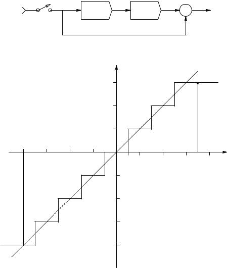
When a Nyquist band-limited analog signal is sampled and then converted by an N bit ADC to digital form, a statistical uncertainty in the digital signal amplitude exists that can be considered to be equivalent to a broadband quantization noise added to the analog signal input before sampling. In the quantization error-generating model of Figure 10.26, a noise-free Nyquist-limited analog signal, vx(t), is sampled and digitized by an N-bit ADC of the round-off type. The ADC’s numerical output, vx*(nT), is the input to an N-bit DAC. The quantization error, e(n), is defined at sampling instants as the difference between the sampled analog input signal, vx(nT), and the analog DAC output, vy(nT). (From now on, the shorter notation, x(n), y(n), etc. will be used.) The ADC/DAC channel has unity gain. Thus the quantization error is simply:
e(n) = x(n) − y(n). |
(10.49) |
Figure 10.27 illustrates a bipolar rounding quantizer function relating analog sampler output, x(n), to the binary DAC output, x*(n). In this example, N = 3. (This uniform rounding quantizer has 2N levels and (2N – 1) steps.) When y(n) is compared to the direct path, the error, e(n), can range over
© 2004 by CRC Press LLC
424 |
|
Analysis and Application of Analog Electronic Circuits |
|||
|
|
Sampler |
|
|
e(n) |
|
x(t) |
x(n) |
x*(n) |
y(n) |
|
|
N-bit ADC |
|
N-bit DAC |
− |
|
|
|
|
|||
|
|
Ts |
|
|
|
|
|
|
|
+ |
|
|
|
|
|
|
|
FIGURE 10.26
A quantization noise error-generating model for an ideal N-bit ADC driving an N-bit ideal DAC.
|
|
|
x*(n) |
|
x*(n) = x(n) |
|
|
|
|
|
111 |
|
|
|
|
|
|
|
110 |
|
|
|
|
|
|
q = Vm /7 |
|
|
|
|
|
|
|
|
101 |
|
|
3Vm /7 |
|
|
|
|
|
|
|
|
|
−4q |
−3q |
−2q |
−q |
|
|
|
x(n) |
|
|
|
100 |
|
|
|
|
|
|
|
|
|
|
|
|
|
|
|
q/2 |
q |
2q |
3q |
4q |
|
|
|
011 |
|
|
|
|
|
|
|
|
|
Vm |
|
|
|
|
|
|
|
q = |
|
|
|
|
|
010 |
|
N − 1 |
) |
|
|
|
|
|
|
(2 |
|
|
|
|
|
|
|
N = 3 |
|
|
−4Vm /7 |
|
|
001 |
|
(7 steps |
|
|
|
|
|
8 levels) |
|
|||
|
|
|
|
|
|
||
|
|
|
000 |
|
|
|
|
FIGURE 10.27
A 3-bit rounding quantizer I/O function.
±q/2 in the center of the range, where q is the voltage step size of the ADC/DAC. It is easy to see that for full dynamic range, q should be:
V
q = ( xMAX ) volts (10.50) 2N − 1
where VxMAX is the maximum (peak-to-peak) value of the input, vx(t), to the ADC/DAC system.
© 2004 by CRC Press LLC

Digital Interfaces |
|
|
425 |
||||
|
|
|
|
pe(e) |
|
|
|
|
|
|
|
|
|
|
|
|
|
|
1/q |
|
|
|
|
|
|
|
|
|
|
e |
|
|
|
|
|
|
|
||
|
|
|
|
|
|
|
|
|
−q/2 |
|
0 |
q/2 |
|||
FIGURE 10.28
The rectangular probability density function generally assumed for quantization noise.
For example, if a 10-bit ADC is used to convert a signal ranging from −5 to +5 V, then by Equation 10.50, q = 9.775 mV. If x(t) has zero mean and its probability density function (PDF) has a standard deviation σx > q, then it can be shown that the PDF of e(n) is well modeled by a uniform (rectangular) density, fe(e), over e = ±q/2. This rectangular PDF is shown in Figure 10.28; it has a peak height of 1/q. The mean-squared error voltage is found from the expectation:
|
|
|
|
• |
|
|
|
q 2 |
|
|
|
1 q |
e |
3 |
|
q 2 |
q |
2 |
2 |
|
|
|
|
|
|
|
|
|
|
|
|
|
|
|
|||||||||
2 |
|
|
2 |
|
2 |
|
|
|
2 |
|
|
|
|
|
|
|
|
||||
|
|
|
|
|
|
|
|
( ) |
|
|
|
|
|
|
|
||||||
E{e |
} = e |
|
= e |
|
fe |
(e)de = |
e |
|
fe |
(e)de = |
|
|
|
|
= |
|
= σq |
msV |
(10.51) |
||
|
|
|
3 |
|
|
12 |
|||||||||||||||
|
|
|
|
−• |
|
|
|
−q 2 |
|
|
|
|
|
|
|
−q 2 |
|
|
|
|
|
|
|
|
|
|
|
|
|
|
|
|
|
|
|
|
|
|
|
|
|||
Thus, it is possible to treat quantization error noise as a zero-mean, broad-band noise with a standard deviation of σq = q/ 12 V, added to the ADC/DAC input signal, x(t). The QN spectral bandwidth is assumed to be flat over ±fs/2, where fs is the sampling frequency, i.e., the Nyquist range.
In order to minimize the effects of quantization noise for an N-bit ADC, it is important that the analog input signal, vx(t), use nearly the full dynamic range of the ADC. In the case of a zero-mean, time-varying signal that is Nyquist band limited, gains and sensitivities should be chosen so that the peak expected x(t) does not exceed the maximum voltage limits of the ADC.
If x(t) is an SRV and has a Gaussian PDF with zero mean, the dynamic range of the ADC should be about ±3 standard deviations of the signal. Under this particular condition, it is possible to derive an expression for the mean-squared signal-to-noise ratio of the ADC and its quantization noise. Let the signal have an RMS value σx volts. From Equation 10.50, the quantization step size can be written:
q ♠ |
( |
6 σx |
) |
volts, |
(10.52) |
||
2N − |
|
||||||
|
1 |
||||||
|
|
|
|
|
|||
or |
|
|
( |
|
|
) |
|
σ |
x |
|
|
|
(10.53) |
||
|
= q 2N − 1 6 |
||||||
© 2004 by CRC Press LLC
426 |
Analysis and Application of Analog Electronic Circuits |
From which it can be seen that σx > q for N ≥ 3. Relation 10.52 for q can be substituted into Equation 10.51 for the variance of the quantization noise. Thus, the mean-squared output noise is:
N = |
q2 |
= |
36 |
σx2 |
|
= |
|
3 σx2 |
|
= σ 2 |
MSV |
(10.54) |
|||
|
( |
|
) |
( |
|
) |
|||||||||
o |
|
|
N |
|
|
|
N |
|
q |
|
|
||||
12 |
|
12 2 |
− 1 |
|
|
2 |
− 1 |
|
|
||||||
|
|
|
|
|
|
|
|
|
|||||||
Thus, the mean-squared signal-to-noise ratio of the N-bit rounding quantizer is:
SNR |
q |
= |
( |
2N − 1 3 MSV MSV |
(10.55) |
|||
|
|
) |
|
|
|
|||
Note that the quantizer SNR is independent |
TABLE 10.1 |
|||||||
of σx as long as σx is held constant under the |
SNR Values for an N-Bit |
|||||||
dynamic range constraint described previ- |
||||||||
ADC Treated as a Quantizer |
||||||||
ously. In dB, SNRq = 10 log[(2N − 1)/3]. Table |
||||||||
|
|
|
||||||
N |
dB SNRq |
|||||||
10.1 summarizes the SNRq of the quantizer for |
||||||||
|
|
|
||||||
different bit values. |
|
|
|
|
6 |
31.2 |
|
|
Because of their low quantization noise, 16- |
8 |
43.4 |
|
|||||
to 24-bit ADCs are routinely used in modern |
10 |
55.4 |
|
|||||
12 |
67.5 |
|
||||||
digital audio systems. Other classes of input |
|
|||||||
14 |
79.5 |
|
||||||
signals to uniform quantizers, such as sine |
|
|||||||
16 |
91.6 |
|
||||||
waves, triangle waves, and narrow-band |
|
|
|
|||||
Note: Total input range is as- |
||||||||
Gaussian noise, are discussed by Kollár (1986). |
||||||||
|
sumed to be 6 σx V. Note |
|||||||
Figure 10.29 illustrates a model whereby |
|
that about 6 dB of SNR |
||||||
the equivalent QN is added to the ideal sam- |
|
improvement occurs for |
||||||
pled signal at the input to some digital filter, |
|
every bit added to the |
||||||
H(z). Note that the quantization error |
|
ADC word length. |
||||||
|
|
|
||||||
sequence, e(n), is assumed to be from a wide- |
|
|
|
|||||
sense stationary white-noise process, where each sample, e(n), is uniformly distributed over the quantization error. The error sequence is also assumed to be uncorrelated with the corresponding input sequence, x(n). Furthermore, the input sequence is assumed to be a sample sequence of a stationary random process, {x}. Note that e(n) is treated as white sampled noise (as opposed to sampled white noise). The auto-power density spectrum of e(n) is assumed to be flat (constant) over the Nyquist range: −π/T ≤ ω ≤ π/T r/s. (T is the sampling period.) e(n) propagates through the digital filter; in the time domain this can be written as a real discrete convolution:
• |
|
y(n) = e(m)h(n − m) |
(10.56) |
m= −•
© 2004 by CRC Press LLC