

- •Analysis and Application of Analog Electronic Circuits to Biomedical Instrumentation
- •Dedication
- •Preface
- •Reader Background
- •Rationale
- •Description of the Chapters
- •Features
- •The Author
- •Table of Contents
- •1.1 Introduction
- •1.2 Sources of Endogenous Bioelectric Signals
- •1.3 Nerve Action Potentials
- •1.4 Muscle Action Potentials
- •1.4.1 Introduction
- •1.4.2 The Origin of EMGs
- •1.5 The Electrocardiogram
- •1.5.1 Introduction
- •1.6 Other Biopotentials
- •1.6.1 Introduction
- •1.6.2 EEGs
- •1.6.3 Other Body Surface Potentials
- •1.7 Discussion
- •1.8 Electrical Properties of Bioelectrodes
- •1.9 Exogenous Bioelectric Signals
- •1.10 Chapter Summary
- •2.1 Introduction
- •2.2.1 Introduction
- •2.2.4 Schottky Diodes
- •2.3.1 Introduction
- •2.4.1 Introduction
- •2.5.1 Introduction
- •2.5.5 Broadbanding Strategies
- •2.6 Photons, Photodiodes, Photoconductors, LEDs, and Laser Diodes
- •2.6.1 Introduction
- •2.6.2 PIN Photodiodes
- •2.6.3 Avalanche Photodiodes
- •2.6.4 Signal Conditioning Circuits for Photodiodes
- •2.6.5 Photoconductors
- •2.6.6 LEDs
- •2.6.7 Laser Diodes
- •2.7 Chapter Summary
- •Home Problems
- •3.1 Introduction
- •3.2 DA Circuit Architecture
- •3.4 CM and DM Gain of Simple DA Stages at High Frequencies
- •3.4.1 Introduction
- •3.5 Input Resistance of Simple Transistor DAs
- •3.7 How Op Amps Can Be Used To Make DAs for Medical Applications
- •3.7.1 Introduction
- •3.8 Chapter Summary
- •Home Problems
- •4.1 Introduction
- •4.3 Some Effects of Negative Voltage Feedback
- •4.3.1 Reduction of Output Resistance
- •4.3.2 Reduction of Total Harmonic Distortion
- •4.3.4 Decrease in Gain Sensitivity
- •4.4 Effects of Negative Current Feedback
- •4.5 Positive Voltage Feedback
- •4.5.1 Introduction
- •4.6 Chapter Summary
- •Home Problems
- •5.1 Introduction
- •5.2.1 Introduction
- •5.2.2 Bode Plots
- •5.5.1 Introduction
- •5.5.3 The Wien Bridge Oscillator
- •5.6 Chapter Summary
- •Home Problems
- •6.1 Ideal Op Amps
- •6.1.1 Introduction
- •6.1.2 Properties of Ideal OP Amps
- •6.1.3 Some Examples of OP Amp Circuits Analyzed Using IOAs
- •6.2 Practical Op Amps
- •6.2.1 Introduction
- •6.2.2 Functional Categories of Real Op Amps
- •6.3.1 The GBWP of an Inverting Summer
- •6.4.3 Limitations of CFOAs
- •6.5 Voltage Comparators
- •6.5.1 Introduction
- •6.5.2. Applications of Voltage Comparators
- •6.5.3 Discussion
- •6.6 Some Applications of Op Amps in Biomedicine
- •6.6.1 Introduction
- •6.6.2 Analog Integrators and Differentiators
- •6.7 Chapter Summary
- •Home Problems
- •7.1 Introduction
- •7.2 Types of Analog Active Filters
- •7.2.1 Introduction
- •7.2.3 Biquad Active Filters
- •7.2.4 Generalized Impedance Converter AFs
- •7.3 Electronically Tunable AFs
- •7.3.1 Introduction
- •7.3.3 Use of Digitally Controlled Potentiometers To Tune a Sallen and Key LPF
- •7.5 Chapter Summary
- •7.5.1 Active Filters
- •7.5.2 Choice of AF Components
- •Home Problems
- •8.1 Introduction
- •8.2 Instrumentation Amps
- •8.3 Medical Isolation Amps
- •8.3.1 Introduction
- •8.3.3 A Prototype Magnetic IsoA
- •8.4.1 Introduction
- •8.6 Chapter Summary
- •9.1 Introduction
- •9.2 Descriptors of Random Noise in Biomedical Measurement Systems
- •9.2.1 Introduction
- •9.2.2 The Probability Density Function
- •9.2.3 The Power Density Spectrum
- •9.2.4 Sources of Random Noise in Signal Conditioning Systems
- •9.2.4.1 Noise from Resistors
- •9.2.4.3 Noise in JFETs
- •9.2.4.4 Noise in BJTs
- •9.3 Propagation of Noise through LTI Filters
- •9.4.2 Spot Noise Factor and Figure
- •9.5.1 Introduction
- •9.6.1 Introduction
- •9.7 Effect of Feedback on Noise
- •9.7.1 Introduction
- •9.8.1 Introduction
- •9.8.2 Calculation of the Minimum Resolvable AC Input Voltage to a Noisy Op Amp
- •9.8.5.1 Introduction
- •9.8.5.2 Bridge Sensitivity Calculations
- •9.8.7.1 Introduction
- •9.8.7.2 Analysis of SNR Improvement by Averaging
- •9.8.7.3 Discussion
- •9.10.1 Introduction
- •9.11 Chapter Summary
- •Home Problems
- •10.1 Introduction
- •10.2 Aliasing and the Sampling Theorem
- •10.2.1 Introduction
- •10.2.2 The Sampling Theorem
- •10.3 Digital-to-Analog Converters (DACs)
- •10.3.1 Introduction
- •10.3.2 DAC Designs
- •10.3.3 Static and Dynamic Characteristics of DACs
- •10.4 Hold Circuits
- •10.5 Analog-to-Digital Converters (ADCs)
- •10.5.1 Introduction
- •10.5.2 The Tracking (Servo) ADC
- •10.5.3 The Successive Approximation ADC
- •10.5.4 Integrating Converters
- •10.5.5 Flash Converters
- •10.6 Quantization Noise
- •10.7 Chapter Summary
- •Home Problems
- •11.1 Introduction
- •11.2 Modulation of a Sinusoidal Carrier Viewed in the Frequency Domain
- •11.3 Implementation of AM
- •11.3.1 Introduction
- •11.3.2 Some Amplitude Modulation Circuits
- •11.4 Generation of Phase and Frequency Modulation
- •11.4.1 Introduction
- •11.4.3 Integral Pulse Frequency Modulation as a Means of Frequency Modulation
- •11.5 Demodulation of Modulated Sinusoidal Carriers
- •11.5.1 Introduction
- •11.5.2 Detection of AM
- •11.5.3 Detection of FM Signals
- •11.5.4 Demodulation of DSBSCM Signals
- •11.6 Modulation and Demodulation of Digital Carriers
- •11.6.1 Introduction
- •11.6.2 Delta Modulation
- •11.7 Chapter Summary
- •Home Problems
- •12.1 Introduction
- •12.2.1 Introduction
- •12.2.2 The Analog Multiplier/LPF PSR
- •12.2.3 The Switched Op Amp PSR
- •12.2.4 The Chopper PSR
- •12.2.5 The Balanced Diode Bridge PSR
- •12.3 Phase Detectors
- •12.3.1 Introduction
- •12.3.2 The Analog Multiplier Phase Detector
- •12.3.3 Digital Phase Detectors
- •12.4 Voltage and Current-Controlled Oscillators
- •12.4.1 Introduction
- •12.4.2 An Analog VCO
- •12.4.3 Switched Integrating Capacitor VCOs
- •12.4.6 Summary
- •12.5 Phase-Locked Loops
- •12.5.1 Introduction
- •12.5.2 PLL Components
- •12.5.3 PLL Applications in Biomedicine
- •12.5.4 Discussion
- •12.6 True RMS Converters
- •12.6.1 Introduction
- •12.6.2 True RMS Circuits
- •12.7 IC Thermometers
- •12.7.1 Introduction
- •12.7.2 IC Temperature Transducers
- •12.8 Instrumentation Systems
- •12.8.1 Introduction
- •12.8.5 Respiratory Acoustic Impedance Measurement System
- •12.9 Chapter Summary
- •References

Feedback, Frequency Response, and Amplifier Stability |
|
223 |
||||
−Kp β(s + a) |
|
(5.52) |
||||
( |
) |
+ |
( |
α2 + γ 2 |
) |
|
AL (s) = s2 + s 2α |
|
|
|
|||
The circle’s radius is now found from the Pythagorean theorem:
R = (a − α)2 + γ 2 |
(5.53) |
Note that as the gain, Kp β, is increased, the closed-loop system poles become more and more damped, until they become real, one approaching the zero at s = –a and the other going to −•.
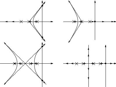
The damping of a complex-conjugate (CC) pole pair in the s-plane can be determined quantitatively by drawing a line from the origin to the upperhalf plane pole. The damping factor, ζ, associated with the CC poles can be shown to be the cosine of the angle that the line from the origin to the CC pole makes with the negative real axis, i.e., ξ = cos(φ). If the poles lie close to the jω axis, φ 90∞ and ξ 0. The length of the line from the origin to one of the CC poles is the undamped natural frequency, ωn, of that CC pole pair. Recall that the CC pole pair is the result of factoring the quadratic term, [s2 + s(2ξωn) + ωn2]. By way of example, the damping of the open-loop CC pole pair in Figure 5.18(B) is ξ = cos[tan−1(γ/α)] = α/ωn.
Many other interesting examples of root-locus plots are to be found in the control systems texts by Kuo (1982) and Ogata (1970) and in the electronic circuits text by Gray and Meyer (1984). Circle root-locus plots are easy to construct graphically by hand. More complex root-locus plots should be done by computer. In closing, it should be stressed that root-locus plots show the closed-loop systems poles. Closed-loop zeros can be found algebraically; they are generally fixed (not functions of gain) and do affect system transient response. Merely locating the closed-loop poles in an apparently good position does not necessarily guarantee a step response without an objectionable overshoot.
Figure 5.19(A) through Figure 5.19(L) illustrate typical root-locus diagrams for linear SISO feedback systems. Locus branches for loop gains with NFB (left column) and for PFB (right column) are shown. The unstable systems oscillate when complex-conjugate closed-loop pole pairs move into the righthalf s-plane; they saturate when one closed-loop pole moves into the right-half s-plane.
5.5Use of Root-Locus in the Design of “Linear” Oscillators
5.5.1Introduction
“Linear” oscillators are used to generate sinusoidal signals for many applications; probably the most important is testing the steady-state sinusoidal
© 2004 by CRC Press LLC
224 |
|
Analysis and Application of Analog Electronic Circuits |
|||||
|
A |
|
|
B |
|
||
|
|
|
|
||||
|
|
|
|
|
|
|
|
|
|
|
|
|
|
|
|
C |
D |
E |
F |
G |
|
H |
|
|
|
|
|
|
FIGURE 5.19
(A) through (L): Representative root-locus plots for six loop gain configurations for NFB and PFB conditions. PFB root-locus plots are on the right.
frequency response of amplifiers. They are also used in measurements as the signal source for ac bridges used to measure the values of circuit components R, L, and C, as well as circuits Z(jω) and Y(jω). Still another oscillator application is a signal source in acoustic measurements. In biomedicine, oscillators are used to power ac current sources in impedance pneumography and plethysmography (Northrop, 2002).
Linear oscillators are called “linear” because the criteria for oscillation are based on linear circuit theory and root locus, which is applied to linear systems. In reality, linear oscillators are designed to have a closed-loop, complex-conjugate pole pair in the right-half s-plane so that oscillations,
© 2004 by CRC Press LLC
Feedback, Frequency Response, and Amplifier Stability |
225 |
I |
J |
K |
L |
FIGURE 5.19 (continued)
when they start, will grow exponentially. Oscillations start because circuit noise voltages or turn-on transients excite the unstable system. To limit and stabilize the amplitude of the output oscillations, a nonlinear mechanism must be used to effectively lower the oscillator’s loop gain to a value that will sustain stable oscillations at some design output amplitude.
Linear oscillators can be designed to use negative or positive voltage feedback. The first to be analyzed is the phase-shift oscillator, which uses NVF.
5.5.2The Phase-Shift Oscillator
A schematic for a phase-shift oscillator (PSO) is shown in Figure 5.20. To simplify analysis, the op amps are treated as ideal. The PSO uses negative feedback applied through an RC filter with transfer function, Vi/Vo = β(s). The second op amp provides an automatic gain control that reduces the oscillator’s loop gain as a function of its output voltage, thus stabilizing the output amplitude. A small tungsten lamp is used as voltage-dependent resistance. As the voltage across the lamp, Vb, increases, its filament heats up (becomes brighter). Metals such as tungsten have positive temperature coefficients, i.e., the filament resistance increases with temperature. Filament temperature is approximately proportional to the lamp’s electrical power input, so the curve of Rb(Vb) is approximately square-law. As the lamp’s voltage increases, so does its resistance, and the gain of the inverting op amp stage decreases as shown in the figure. The second op amp’s gain is:
© 2004 by CRC Press LLC

226 |
Analysis and Application of Analog Electronic Circuits |
||||
|
|
RF |
|
|
R2 |
|
|
|
|
|
|
R1 |
|
|
|
Rb |
|
|
|
|
|
|
|
|
|
IOA |
Vb |
Bulb (0) |
Vo |
|
|
|
|
IOA |
|
|
C |
C |
C |
Vo |
|
Vi |
|
V2 |
V1 |
|
|
R |
|
R |
R |
|
|
Av2 |
Rb |
−R2 /Rbo
−1 |
|
RbQ |
|
|
|
|
|
||
|
Vb |
Rbo |
Vb |
|
0 0 |
0 0 |
|||
VbQ |
VbQ |
FIGURE 5.20
Top: schematic of an R–C phase-shift oscillator that uses NFB. The lamp is used as a nonlinear resistance to limit oscillation amplitude. Bottom left: gain of the right-hand op amp stage as a function of the RMS Vb across the bulb. Bottom right: resistance of the lamp as a function of the RMS Vb. The resistance increase is due to the tungsten filament heating.
Vo |
= A |
= |
R2 |
(5.54) |
|
Rb (vb ) |
|||
Vb |
v2 |
|
|
|
|
|
|
R2 is made equal to the desired Rb = RbQ at the desired Vb = VbQ, so Av2 = −1 when Vb = VbQ . If Vb > VbQ , then Av2 < 1. The gain of the first (noninverting) op amp stage is simply Vb /Vi = (1 + RF/R1) = Av1.
The gain of the feedback circuit is found by writing the three node equations for the circuit:
|
V1(s2C + G) − V2 sC + 0 = Vo sC |
(5.55A) |
||
|
−V1sC + V2 (s2C + G) − Vi sC = 0 |
(5.55B) |
||
|
|
0 − V2 sC + Vi (sC + G) = 0 |
(5.55C) |
|
Using Cramer’s rule, solve for β(s) = Vi/Vo: |
|
|||
β(s) = |
V |
= |
s3 |
(5.56) |
i |
|
|||
Vo |
s3 + s2 6 (RC) + s 5 (RC)2 + 1 (RC)3 |
|||
© 2004 by CRC Press LLC
Feedback, Frequency Response, and Amplifier Stability |
227 |
The three roots of β(s) are real and negative, i.e., they lie on the negative real axis in the s-plane. Their vector values are found with Matlab’s ROOTS utility: s1 = −5.0489/(RC), s2 = −0.6431/(RC) and s3 = −0.3080/(RC). The PS oscillator’s loop gain as a function of frequency is, in vector form,
A (s) = |
−s3 (1+ RF R1)(R2 Rb ) |
= |
−A3 (1+ RF R1)(R2 Rb ) |
(5.57) |
|
(s − s1 )(s − s2 )(s − s3 ) |
BC D |
||||
L |
|
|
|||
|
|
|
|
Alternately, AL can be written as an unfactored frequency response polynomial:
AL (jω) = |
|
(jω3 )(1+ RF R1)(R2 Rb ) |
|
|
(5.58) |
||
− jω3 |
− ω2 6 (RC) + jω 5 (RC) |
2 |
+ 1 |
(RC) |
3 |
||
|
|
|
|
||||
The Barkhausen criterion can be used to find the frequency of oscillation, ωo, and the critical gain required for a pair of the oscillator’s closed-loop, complex-conjugate poles to lie on the jω axis in the s-plane. To apply the complex algebraic Barkhausen criterion, set AL(jωo) = 1–0∞ and note that, for AL(jωo) to be real, the real part of its denominator must equal zero. From this condition,
−ωo2 6 (RC) + 1 (RC)3 = 0 |
|
(5.59) |
|
The oscillation frequency is: |
|
|
|
ωo = 1 |
( 6 RC) = 0.40825 (RC) |
r s |
(5.60) |
The critical gain is found by setting |
|
|
|
AL (jωo ) = |
(− jωo3 )(1+ RF R1)(R2 Rb ) |
= 1+ j0 |
(5.61) |
− jωo3 + jωo 5 (RC)2 |
|||
and solving for (1 + RF/R1)(R2/Rb). Thus:
(1+ RF R1)(R2 Rb ) = 29 |
(5.62) |
For oscillations to start, Vb 0, and (1 + RF/R1)(R2/Rbo) must be >29, so the system’s poles will be in the right-half s-plane and the oscillations (and Vb ) will grow exponentially. When Vb reaches VbQ, R2/Rb = R2/RbQ = 1, (1 + RF /R1)(R2/Rb) = 1, and the PS oscillator’s poles are at s = ±jωo, giving stable oscillations with Vo = VbQ.
© 2004 by CRC Press LLC