

- •Analysis and Application of Analog Electronic Circuits to Biomedical Instrumentation
- •Dedication
- •Preface
- •Reader Background
- •Rationale
- •Description of the Chapters
- •Features
- •The Author
- •Table of Contents
- •1.1 Introduction
- •1.2 Sources of Endogenous Bioelectric Signals
- •1.3 Nerve Action Potentials
- •1.4 Muscle Action Potentials
- •1.4.1 Introduction
- •1.4.2 The Origin of EMGs
- •1.5 The Electrocardiogram
- •1.5.1 Introduction
- •1.6 Other Biopotentials
- •1.6.1 Introduction
- •1.6.2 EEGs
- •1.6.3 Other Body Surface Potentials
- •1.7 Discussion
- •1.8 Electrical Properties of Bioelectrodes
- •1.9 Exogenous Bioelectric Signals
- •1.10 Chapter Summary
- •2.1 Introduction
- •2.2.1 Introduction
- •2.2.4 Schottky Diodes
- •2.3.1 Introduction
- •2.4.1 Introduction
- •2.5.1 Introduction
- •2.5.5 Broadbanding Strategies
- •2.6 Photons, Photodiodes, Photoconductors, LEDs, and Laser Diodes
- •2.6.1 Introduction
- •2.6.2 PIN Photodiodes
- •2.6.3 Avalanche Photodiodes
- •2.6.4 Signal Conditioning Circuits for Photodiodes
- •2.6.5 Photoconductors
- •2.6.6 LEDs
- •2.6.7 Laser Diodes
- •2.7 Chapter Summary
- •Home Problems
- •3.1 Introduction
- •3.2 DA Circuit Architecture
- •3.4 CM and DM Gain of Simple DA Stages at High Frequencies
- •3.4.1 Introduction
- •3.5 Input Resistance of Simple Transistor DAs
- •3.7 How Op Amps Can Be Used To Make DAs for Medical Applications
- •3.7.1 Introduction
- •3.8 Chapter Summary
- •Home Problems
- •4.1 Introduction
- •4.3 Some Effects of Negative Voltage Feedback
- •4.3.1 Reduction of Output Resistance
- •4.3.2 Reduction of Total Harmonic Distortion
- •4.3.4 Decrease in Gain Sensitivity
- •4.4 Effects of Negative Current Feedback
- •4.5 Positive Voltage Feedback
- •4.5.1 Introduction
- •4.6 Chapter Summary
- •Home Problems
- •5.1 Introduction
- •5.2.1 Introduction
- •5.2.2 Bode Plots
- •5.5.1 Introduction
- •5.5.3 The Wien Bridge Oscillator
- •5.6 Chapter Summary
- •Home Problems
- •6.1 Ideal Op Amps
- •6.1.1 Introduction
- •6.1.2 Properties of Ideal OP Amps
- •6.1.3 Some Examples of OP Amp Circuits Analyzed Using IOAs
- •6.2 Practical Op Amps
- •6.2.1 Introduction
- •6.2.2 Functional Categories of Real Op Amps
- •6.3.1 The GBWP of an Inverting Summer
- •6.4.3 Limitations of CFOAs
- •6.5 Voltage Comparators
- •6.5.1 Introduction
- •6.5.2. Applications of Voltage Comparators
- •6.5.3 Discussion
- •6.6 Some Applications of Op Amps in Biomedicine
- •6.6.1 Introduction
- •6.6.2 Analog Integrators and Differentiators
- •6.7 Chapter Summary
- •Home Problems
- •7.1 Introduction
- •7.2 Types of Analog Active Filters
- •7.2.1 Introduction
- •7.2.3 Biquad Active Filters
- •7.2.4 Generalized Impedance Converter AFs
- •7.3 Electronically Tunable AFs
- •7.3.1 Introduction
- •7.3.3 Use of Digitally Controlled Potentiometers To Tune a Sallen and Key LPF
- •7.5 Chapter Summary
- •7.5.1 Active Filters
- •7.5.2 Choice of AF Components
- •Home Problems
- •8.1 Introduction
- •8.2 Instrumentation Amps
- •8.3 Medical Isolation Amps
- •8.3.1 Introduction
- •8.3.3 A Prototype Magnetic IsoA
- •8.4.1 Introduction
- •8.6 Chapter Summary
- •9.1 Introduction
- •9.2 Descriptors of Random Noise in Biomedical Measurement Systems
- •9.2.1 Introduction
- •9.2.2 The Probability Density Function
- •9.2.3 The Power Density Spectrum
- •9.2.4 Sources of Random Noise in Signal Conditioning Systems
- •9.2.4.1 Noise from Resistors
- •9.2.4.3 Noise in JFETs
- •9.2.4.4 Noise in BJTs
- •9.3 Propagation of Noise through LTI Filters
- •9.4.2 Spot Noise Factor and Figure
- •9.5.1 Introduction
- •9.6.1 Introduction
- •9.7 Effect of Feedback on Noise
- •9.7.1 Introduction
- •9.8.1 Introduction
- •9.8.2 Calculation of the Minimum Resolvable AC Input Voltage to a Noisy Op Amp
- •9.8.5.1 Introduction
- •9.8.5.2 Bridge Sensitivity Calculations
- •9.8.7.1 Introduction
- •9.8.7.2 Analysis of SNR Improvement by Averaging
- •9.8.7.3 Discussion
- •9.10.1 Introduction
- •9.11 Chapter Summary
- •Home Problems
- •10.1 Introduction
- •10.2 Aliasing and the Sampling Theorem
- •10.2.1 Introduction
- •10.2.2 The Sampling Theorem
- •10.3 Digital-to-Analog Converters (DACs)
- •10.3.1 Introduction
- •10.3.2 DAC Designs
- •10.3.3 Static and Dynamic Characteristics of DACs
- •10.4 Hold Circuits
- •10.5 Analog-to-Digital Converters (ADCs)
- •10.5.1 Introduction
- •10.5.2 The Tracking (Servo) ADC
- •10.5.3 The Successive Approximation ADC
- •10.5.4 Integrating Converters
- •10.5.5 Flash Converters
- •10.6 Quantization Noise
- •10.7 Chapter Summary
- •Home Problems
- •11.1 Introduction
- •11.2 Modulation of a Sinusoidal Carrier Viewed in the Frequency Domain
- •11.3 Implementation of AM
- •11.3.1 Introduction
- •11.3.2 Some Amplitude Modulation Circuits
- •11.4 Generation of Phase and Frequency Modulation
- •11.4.1 Introduction
- •11.4.3 Integral Pulse Frequency Modulation as a Means of Frequency Modulation
- •11.5 Demodulation of Modulated Sinusoidal Carriers
- •11.5.1 Introduction
- •11.5.2 Detection of AM
- •11.5.3 Detection of FM Signals
- •11.5.4 Demodulation of DSBSCM Signals
- •11.6 Modulation and Demodulation of Digital Carriers
- •11.6.1 Introduction
- •11.6.2 Delta Modulation
- •11.7 Chapter Summary
- •Home Problems
- •12.1 Introduction
- •12.2.1 Introduction
- •12.2.2 The Analog Multiplier/LPF PSR
- •12.2.3 The Switched Op Amp PSR
- •12.2.4 The Chopper PSR
- •12.2.5 The Balanced Diode Bridge PSR
- •12.3 Phase Detectors
- •12.3.1 Introduction
- •12.3.2 The Analog Multiplier Phase Detector
- •12.3.3 Digital Phase Detectors
- •12.4 Voltage and Current-Controlled Oscillators
- •12.4.1 Introduction
- •12.4.2 An Analog VCO
- •12.4.3 Switched Integrating Capacitor VCOs
- •12.4.6 Summary
- •12.5 Phase-Locked Loops
- •12.5.1 Introduction
- •12.5.2 PLL Components
- •12.5.3 PLL Applications in Biomedicine
- •12.5.4 Discussion
- •12.6 True RMS Converters
- •12.6.1 Introduction
- •12.6.2 True RMS Circuits
- •12.7 IC Thermometers
- •12.7.1 Introduction
- •12.7.2 IC Temperature Transducers
- •12.8 Instrumentation Systems
- •12.8.1 Introduction
- •12.8.5 Respiratory Acoustic Impedance Measurement System
- •12.9 Chapter Summary
- •References
338 |
|
Analysis and Application of Analog Electronic Circuits |
||
|
|
SnW |
|
|
|
|
(MSV/Hz) |
|
. . . |
|
η |
|
||
|
|
f (Hz) |
||
|
|
|
||
0
0
A
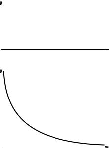
Sn(f) = b/f n
(MSV/Hz)
f (Hz)
0
0
B
FIGURE 9.2
(A) A one-sided, white-noise power density spectrum. (B) A one-sided, one-over-f power density spectrum. Both of these spectra are idealized mathematical models. Their integrals are infinite.
9.2.4Sources of Random Noise in Signal Conditioning Systems
Sources of random noise in signal conditioning systems can be separated into two major categories: noise from passive resistors and noise from semiconductor circuit elements such as bipolar junction transistors, field-effect transistors, and diodes. In most cases, the Gaussian assumption for noise amplitude PDFs is valid and the noise generated can generally be assumed to have a white (flat) power over a major portion of its spectrum.
9.2.4.1Noise from Resistors
From statistical mechanics, it can be shown that any pure resistance at some temperature T Kelvins will have a zero-mean broadband noise voltage associated with it. This noise voltage appears in series with the (noiseless) resistor as a Thevenin equivalent voltage source. From dc to radio frequencies where the resistor’s capacitance to ground and its lead inductance can no longer be neglected, the resistor’s noise is well modeled by a Gaussian white noise source.
Noise from resistors is called thermal or Johnson noise; its one-sided white PDS is given by the well-known relation:
© 2004 by CRC Press LLC
Noise and the Design of Low-Noise Amplifiers for Biomedical Applications |
339 |
Sn(f ) = 4kTR mean squared volts/Hertz |
(9.23) |
where k is Boltzmann’s constant (1.380 ∞ 10–23 joule/Kelvin), T is in degrees Kelvin, and R is in ohms. In a given noise bandwidth, B = f2 − f1, the mean squared white noise from a resistor can be written:
|
|
f |
|
|
|
|
(B) = 2 |
Sn (f )df = 4kTR(f2 − f1) = 4kTRB MSV |
|
von2 |
(9.24) |
|||
|
|
f1 |
|
|
A Norton equivalent of the Thevenin Johnson noise source from a resistor can be formed by assuming an MS, white noise, short-circuit current source with PDS:
Sni(f ) = 4kTG MS amps/Hz |
(9.25) |
This Norton noise current root spectrum, in RMS A/ Hz, is in parallel with a noiseless conductance, G = 1/R.
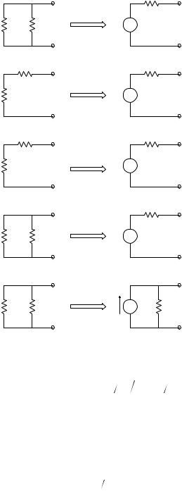
The Johnson noise from several resistors connected in a network may be combined into a single Thevenin noise voltage source in series with a single noiseless equivalent resistor. Figure 9.3 illustrates some of these reductions for two-terminal circuits.
It has been observed that when dc (or average) current is passed through a resistor, the basic Johnson noise PDS is modified by the addition of a lowfrequency, 1/f spectral component, e.g.,
Sn(f ) = 4kTR + A I2/f MSV/Hz |
(9.26) |
where I is the average or dc component of current through the resistor and A is a constant that depends on the material from which the resistor is constructed (e.g., carbon composition, resistance wire, metal film, etc.).
An important parameter for resistors carrying average current is the crossover frequency, fc, where the 1/f PDS equals the PDS of the Johnson noise. fc is easily shown to be:
fc = A I2/4kTR Hz |
(9.27) |
It is possible to show that the fc of a noisy resistor can be reduced by using a resistor of the same type, but with a higher wattage or power dissipation rating. As an example of this principle, consider the circuit of Figure 9.4 in which a single resistor of R ohms, carrying a dc current I, is replaced by nine resistors of resistance R connected in a series-parallel circuit that also carries the current I. The nine-resistor circuit has a net resistance, R, which dissipates nine times the power of the single resistor R. The noise PDS in any one of the nine resistors is:
© 2004 by CRC Press LLC
340 |
|
Analysis and Application of Analog Electronic Circuits |
|
|
|
R1 |
R2 |
R1 @ T |
R2 @ T |
vn |
Sn(f) = 4kT(R1 R2 ) |
|
|
|
MSV/Hz |
|
R2 @ T |
(R1 + R2) |
|
R1 @ T |
|
vn |
Sn(f) = 4kT(R1 + R2) |
|
R2 @ T2 |
(R1 + R2) |
|
R1 @ T1 |
|
vn |
Sn(f) = 4kT(R1T1 + R2T2) |
|
|
(R1 R2 ) |
|
R1 @ T1 |
R2 @ T2 |
vn |
Sn(f) = 4kT1R1 [R2 /(R1 + R2)]2 + |
4kT2R2 [R1 /(R1 + R2)]2 |
|||
R1 @ T1 |
R2 @ T2 |
in |
Sn(f) = 4kT1G1 + 4kT2G2 |
|
MSA/Hz |
||||
|
|
|
||
|
|
|
(R1 R2 ) |
FIGURE 9.3
Examples of combining white Johnson noise power density spectra from pairs of resistors. In the resulting Thevenin models, the Thevenin resistors are noiseless.
n ( |
) |
( |
) |
2 f MSV Hz |
(9.28) |
S′ f |
|
= 4kTR + A I 3 |
|
Each of the nine PDSs given by the preceding equation contributes to the net PDS seen at the terminals of the composite 9-W resistor. Each resistor’s equivalent noise voltage source “sees” a voltage divider formed by the other eight resistors in the composite resistor. The attenuation of each of the nine voltage dividers is given by
3R 2 |
= 1 3 |
(9.29) |
|
3R 2 + 3R |
|||
|
|
© 2004 by CRC Press LLC

Noise and the Design of Low-Noise Amplifiers for Biomedical Applications |
341 |
All resistors R @ T |
|
FIGURE 9.4
Nine identical resistors in series parallel have the same resistance as any one resistor, and nine times the wattage.
The net voltage PDS at the composite resistor’s terminals may only be found by superposition of MS voltages or PDSs:
n(9) |
|
9 |
|
] |
|
(f ) = |
[ |
4kTR + A(I 3)2 |
|
||
S |
|
f (1 3)2 = 4kTR + A I2 9f MSV Hz |
(9.30) |
j =1
Thus, the composite 9-W resistor enjoys a ninefold reduction in the 1/f spectral energy because the dc current density through each element is reduced by one third. The Johnson noise PDS remains the same, however. It is safe to generalize that the use of high wattage resistors of a given type and resistance will result in reduced 1/f noise generation when the resistor carries dc (average) current. The cost of this noise reduction is the extra volume required for a high-wattage resistor and its extra expense.
9.2.4.2The Two-Source Noise Model for Active Devices
Noise arising in JFETs, BJTs, and complex IC amplifiers is generally described by the two-noise source input model. The total noise observed at the output of an amplifier, given that its input terminals are short-circuited, is accounted for by defining an equivalent short-circuited input noise voltage, ena, which replaces the combined effect of all internal noise sources seen at the amplifier’s output under short-circuited input conditions. The amplifier, shown in Figure 9.5, is now considered noiseless. ena is specified by manufacturers for many low-noise discrete transistors and IC amplifiers. ena is a root PDS, i.e., it is the square root of a one-sided PDS and is thus a function of frequency; ena has the units of RMS volts per root Hertz. Figure 9.6 illustrates a plot of a typical ena(f ) vs. f for a low-noise JFET. Also shown in Figure 9.6 is a plot of ina(f ) vs. f for the same device.
© 2004 by CRC Press LLC