

- •Analysis and Application of Analog Electronic Circuits to Biomedical Instrumentation
- •Dedication
- •Preface
- •Reader Background
- •Rationale
- •Description of the Chapters
- •Features
- •The Author
- •Table of Contents
- •1.1 Introduction
- •1.2 Sources of Endogenous Bioelectric Signals
- •1.3 Nerve Action Potentials
- •1.4 Muscle Action Potentials
- •1.4.1 Introduction
- •1.4.2 The Origin of EMGs
- •1.5 The Electrocardiogram
- •1.5.1 Introduction
- •1.6 Other Biopotentials
- •1.6.1 Introduction
- •1.6.2 EEGs
- •1.6.3 Other Body Surface Potentials
- •1.7 Discussion
- •1.8 Electrical Properties of Bioelectrodes
- •1.9 Exogenous Bioelectric Signals
- •1.10 Chapter Summary
- •2.1 Introduction
- •2.2.1 Introduction
- •2.2.4 Schottky Diodes
- •2.3.1 Introduction
- •2.4.1 Introduction
- •2.5.1 Introduction
- •2.5.5 Broadbanding Strategies
- •2.6 Photons, Photodiodes, Photoconductors, LEDs, and Laser Diodes
- •2.6.1 Introduction
- •2.6.2 PIN Photodiodes
- •2.6.3 Avalanche Photodiodes
- •2.6.4 Signal Conditioning Circuits for Photodiodes
- •2.6.5 Photoconductors
- •2.6.6 LEDs
- •2.6.7 Laser Diodes
- •2.7 Chapter Summary
- •Home Problems
- •3.1 Introduction
- •3.2 DA Circuit Architecture
- •3.4 CM and DM Gain of Simple DA Stages at High Frequencies
- •3.4.1 Introduction
- •3.5 Input Resistance of Simple Transistor DAs
- •3.7 How Op Amps Can Be Used To Make DAs for Medical Applications
- •3.7.1 Introduction
- •3.8 Chapter Summary
- •Home Problems
- •4.1 Introduction
- •4.3 Some Effects of Negative Voltage Feedback
- •4.3.1 Reduction of Output Resistance
- •4.3.2 Reduction of Total Harmonic Distortion
- •4.3.4 Decrease in Gain Sensitivity
- •4.4 Effects of Negative Current Feedback
- •4.5 Positive Voltage Feedback
- •4.5.1 Introduction
- •4.6 Chapter Summary
- •Home Problems
- •5.1 Introduction
- •5.2.1 Introduction
- •5.2.2 Bode Plots
- •5.5.1 Introduction
- •5.5.3 The Wien Bridge Oscillator
- •5.6 Chapter Summary
- •Home Problems
- •6.1 Ideal Op Amps
- •6.1.1 Introduction
- •6.1.2 Properties of Ideal OP Amps
- •6.1.3 Some Examples of OP Amp Circuits Analyzed Using IOAs
- •6.2 Practical Op Amps
- •6.2.1 Introduction
- •6.2.2 Functional Categories of Real Op Amps
- •6.3.1 The GBWP of an Inverting Summer
- •6.4.3 Limitations of CFOAs
- •6.5 Voltage Comparators
- •6.5.1 Introduction
- •6.5.2. Applications of Voltage Comparators
- •6.5.3 Discussion
- •6.6 Some Applications of Op Amps in Biomedicine
- •6.6.1 Introduction
- •6.6.2 Analog Integrators and Differentiators
- •6.7 Chapter Summary
- •Home Problems
- •7.1 Introduction
- •7.2 Types of Analog Active Filters
- •7.2.1 Introduction
- •7.2.3 Biquad Active Filters
- •7.2.4 Generalized Impedance Converter AFs
- •7.3 Electronically Tunable AFs
- •7.3.1 Introduction
- •7.3.3 Use of Digitally Controlled Potentiometers To Tune a Sallen and Key LPF
- •7.5 Chapter Summary
- •7.5.1 Active Filters
- •7.5.2 Choice of AF Components
- •Home Problems
- •8.1 Introduction
- •8.2 Instrumentation Amps
- •8.3 Medical Isolation Amps
- •8.3.1 Introduction
- •8.3.3 A Prototype Magnetic IsoA
- •8.4.1 Introduction
- •8.6 Chapter Summary
- •9.1 Introduction
- •9.2 Descriptors of Random Noise in Biomedical Measurement Systems
- •9.2.1 Introduction
- •9.2.2 The Probability Density Function
- •9.2.3 The Power Density Spectrum
- •9.2.4 Sources of Random Noise in Signal Conditioning Systems
- •9.2.4.1 Noise from Resistors
- •9.2.4.3 Noise in JFETs
- •9.2.4.4 Noise in BJTs
- •9.3 Propagation of Noise through LTI Filters
- •9.4.2 Spot Noise Factor and Figure
- •9.5.1 Introduction
- •9.6.1 Introduction
- •9.7 Effect of Feedback on Noise
- •9.7.1 Introduction
- •9.8.1 Introduction
- •9.8.2 Calculation of the Minimum Resolvable AC Input Voltage to a Noisy Op Amp
- •9.8.5.1 Introduction
- •9.8.5.2 Bridge Sensitivity Calculations
- •9.8.7.1 Introduction
- •9.8.7.2 Analysis of SNR Improvement by Averaging
- •9.8.7.3 Discussion
- •9.10.1 Introduction
- •9.11 Chapter Summary
- •Home Problems
- •10.1 Introduction
- •10.2 Aliasing and the Sampling Theorem
- •10.2.1 Introduction
- •10.2.2 The Sampling Theorem
- •10.3 Digital-to-Analog Converters (DACs)
- •10.3.1 Introduction
- •10.3.2 DAC Designs
- •10.3.3 Static and Dynamic Characteristics of DACs
- •10.4 Hold Circuits
- •10.5 Analog-to-Digital Converters (ADCs)
- •10.5.1 Introduction
- •10.5.2 The Tracking (Servo) ADC
- •10.5.3 The Successive Approximation ADC
- •10.5.4 Integrating Converters
- •10.5.5 Flash Converters
- •10.6 Quantization Noise
- •10.7 Chapter Summary
- •Home Problems
- •11.1 Introduction
- •11.2 Modulation of a Sinusoidal Carrier Viewed in the Frequency Domain
- •11.3 Implementation of AM
- •11.3.1 Introduction
- •11.3.2 Some Amplitude Modulation Circuits
- •11.4 Generation of Phase and Frequency Modulation
- •11.4.1 Introduction
- •11.4.3 Integral Pulse Frequency Modulation as a Means of Frequency Modulation
- •11.5 Demodulation of Modulated Sinusoidal Carriers
- •11.5.1 Introduction
- •11.5.2 Detection of AM
- •11.5.3 Detection of FM Signals
- •11.5.4 Demodulation of DSBSCM Signals
- •11.6 Modulation and Demodulation of Digital Carriers
- •11.6.1 Introduction
- •11.6.2 Delta Modulation
- •11.7 Chapter Summary
- •Home Problems
- •12.1 Introduction
- •12.2.1 Introduction
- •12.2.2 The Analog Multiplier/LPF PSR
- •12.2.3 The Switched Op Amp PSR
- •12.2.4 The Chopper PSR
- •12.2.5 The Balanced Diode Bridge PSR
- •12.3 Phase Detectors
- •12.3.1 Introduction
- •12.3.2 The Analog Multiplier Phase Detector
- •12.3.3 Digital Phase Detectors
- •12.4 Voltage and Current-Controlled Oscillators
- •12.4.1 Introduction
- •12.4.2 An Analog VCO
- •12.4.3 Switched Integrating Capacitor VCOs
- •12.4.6 Summary
- •12.5 Phase-Locked Loops
- •12.5.1 Introduction
- •12.5.2 PLL Components
- •12.5.3 PLL Applications in Biomedicine
- •12.5.4 Discussion
- •12.6 True RMS Converters
- •12.6.1 Introduction
- •12.6.2 True RMS Circuits
- •12.7 IC Thermometers
- •12.7.1 Introduction
- •12.7.2 IC Temperature Transducers
- •12.8 Instrumentation Systems
- •12.8.1 Introduction
- •12.8.5 Respiratory Acoustic Impedance Measurement System
- •12.9 Chapter Summary
- •References
Noise and the Design of Low-Noise Amplifiers for Biomedical Applications |
365 |
|
Vo = 3 enμ (enμ is the thermal noise from Rμ.) |
(9.103A) |
|
Vo = 3Rμ ina |
(9.103B) |
|
Vo = ena 3[1 + sRμ(3CT/2)] |
(9.103C) |
|
The total MS noise output of the C-neut. amp is found by superposition of the three mean-squared noise components:
No = {9(4kTRμ )+ 9 Rμ2 ina2}B + B |
9 ena2 |
|
1+ j2πfRμ (3CT |
2) |
|
2 df MSV (9.104A) |
|||||||||||||||
|
|
||||||||||||||||||||
|
|
|
|
|
|
|
|||||||||||||||
|
|
|
|
|
|
0 |
|
|
|
|
|
|
|
|
|
|
|
|
|
|
|
|
|
|
|
|
|
|
¬ |
|
|
|
|
|
|
|
|
|
|
|
|
|
|
N |
= |
( |
4kTR |
) |
+ R2 i 2 |
+ e 2 9B + 9e 2 |
( |
B3 |
3 |
) |
2πR |
( |
3C |
2 |
) |
2 |
MSV (9.104B) |
||||
|
|||||||||||||||||||||
o |
|
μ |
μ na |
na } |
na |
|
|
μ |
|
T |
|
|
|
|
|||||||
|
{ |
|
|
|
|
|
[ |
|
|
|
|
] |
|
||||||||
The fourth term in Equation 9.104B represents excess noise introduced by the positive feedback through the neutralizing capacitor. B is the Hertz noise bandwidth of the unity-gain ideal low-pass filter used to limit the output noise. Calculating the RMS output noise of the neutralized amplifier: the parameters are amplifier gain = 3; ena = 35 nV RMS/ Hz (white); ina = 1.1 ∞ 10−16 A RMS/ Hz (white); Rμ = 108 Ω; CT = 5 pF; 4kT = 1.656 ∞ 10−20; and B = 5E3 Hz. When substituted into Equation 9.104B, von = 2.915 ∞ 10−4 V RMS, or about 0.3 mV RMS. The corner frequency for the output noise due to ena under conditions of neutralization is:
fc = 1 [2πRμ (3CT 2)] Hz |
(9.105) |
Numerically, this is 212 Hz.
Finally, the SNRo of the neutralized amplifier can be written:
SNRo |
= |
|
|
|
|
|
|
V2 |
|
|
|
|
|
|
|
|
|
|
|
(9.106) |
|
|
|
|
|
|
b |
|
|
|
|
|
|
|
|
|
|
|
|||
( |
|
) |
+ R2 i 2 |
+ e 2 |
|
B + e 2 |
( |
B3 |
|
) |
|
2πR |
( |
|
|
) |
2 |
|||
|
|
{ |
4kTR |
|
} |
|
3 |
|
[ |
|
3C |
2 |
] |
|
||||||
|
|
μ |
|
μ na |
na |
na |
|
|
|
|
μ |
|
T |
|
|
|||||
As a final exercise, find the RMS Vb required to give an MS SNRo = 9. Substituting the preceding numerical values, Vb = 8.75 ∞ 10−4 V RMS.
9.8.5 Calculation of the Smallest Resolvable R/R in a Wheatstone Bridge Determined by Noise
9.8.5.1Introduction
The Wheatstone bridge is typically associated with the precision measurement of resistance. However, this simple ubiquitous circuit is used as an
© 2004 by CRC Press LLC
366 |
Analysis and Application of Analog Electronic Circuits |
||||
R |
R − ∆R |
|
|
|
|
|
ena |
|
QBPF |
|
|
|
|
|
|
||
vs(t) |
|
vi |
|
|
|
|
|
|
|
|
|
|
|
DA |
Vo’ |
jω(2ζ/ωn) |
Vo |
R |
|
|
|
|
|
R + ∆R |
vi’ |
|
(jω)2 /ωn2 + jω(2ζ/ωn) + 1 |
|
|
vs(t) = VS sin(ωn t)
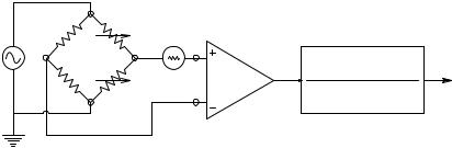
FIGURE 9.19
Schematic of a DA and BPF used to condition the ac output of a two-active arm Wheatstone bridge. The thermal noise from the bridge resistors is assumed white, as is the DA’s ena. The quadratic BPF is used to limit the output noise far from ωn.
output transducer in many biomedical measurement systems in which the quantity under measurement (QUM) causes a sensor to change resistance. Some examples of variable resistance sensors include: thermistors; platinum resistance thermometers; photoconductors; strain gauges; hot-wire anemometers; and direct resistance change by mechanical motion (potentiometers). Bridges used with R sensors generally have ac sources for increased sensitivity. The bridge output under ac excitation can be shown to be doublesideband, suppressed-carrier (DSBSC) modulated ac (Northrop, 1997). DSBSC operation allows enhanced detection sensitivity and noise reduction by band-pass filtering.
9.8.5.2Bridge Sensitivity Calculations
Figure 9.19 illustrates a Wheatstone bridge with an output conditioned by a noisy but otherwise ideal DA. The ac output of the bridge is then passed through a simple quadratic band-pass filter to reduce noise and demodulated by a phase-sensitive rectifier/low-pass filter to give an analog voltage proportional to the QUM causing the sensor’s R. The system appears complex, but in reality is exquisitely sensitive.
In the bridge, two arms are fixed with resistance R and two vary with the QUM — one increasing (R + R) and the other decreasing (R − R), a situation often found in strain gauge systems used in blood pressure sensors. Five sources of white noise are in the circuit: the amplifier’s ena and the thermal noise from the four bridge resistors. It is assumed that the DA has
• CMRR. The voltage at the left-hand corner of the bridge is: v1′ = vs/2. The
voltage at the right-hand corner is v1 = (vs/2)(1 + |
R/R). The voltage at the |
|
DA output is thus: |
|
|
vo′ = Kd (v1 − v1′) = Kd (vs/2)( |
R/R) |
(9.107) |
vs(t) = Vs sin(2πfs t) |
|
(9.108) |
© 2004 by CRC Press LLC

Noise and the Design of Low-Noise Amplifiers for Biomedical Applications |
367 |
vo′ passes through the BPF with unity gain, so the MS output due to R/R is:
os |
( s |
) |
[ |
d |
|
] |
|
|
v 2 |
= V2 |
2 (1 4) |
K |
( |
R R) 2 |
MSV |
(9.109) |
|
9.8.5.3Bridge SNRo
The noise power density spectrum at the DA output is found by superposition of PDSs:
S ′ (f ) = [4kTR/2 + 4kTR/2 + e 2 |
] K 2 |
MSV/Hz (white) (9.110) |
|
no |
na |
d |
|
The gain2-bandwith integral for the unity-gain quadratic BPF with Q = 1/2ξ has been shown to be (2πfs/2Q) Hz. Thus, the MS noise at the filter output is:
|
|
= [4kTR + ena2 ]Kd2 (2πfs 2Q) MSV |
|
|||||||||
|
von2 |
(9.111) |
||||||||||
and the SNRo is: |
|
|
|
|
[ |
|
|
] |
|
|
||
|
|
|
|
|
( s |
) |
d |
|
|
|
||
|
SNRo = |
V2 |
2 (1 4) |
K |
( R R) 2 |
|
||||||
|
[4kTR + ena2 ]Kd2 (2πfs 2Q) |
|
(9.112) |
|||||||||
Equation 9.112 can be used to find the numerical |
R/R required to give a |
|||||||||||
SNRo = 1. Let fs = 1 kHz; 4kT = 1.656 ∞ 10−20; Q = 2; ena = 10 nVRMS/ Hz; |
||||||||||||
R = 400 Ω; K = 103; and V |
s |
= 5 Vpk. From these values, |
R/R is found to |
|||||||||
d |
|
|
|
|
|
|
|
|
|
|||
be 2.315 ∞ 10−7 and R = 0.2315 mΩ. Also, the DA output is 0.579 mVpk.
If a sensor’s sensitivity (e.g., for a blood pressure sensor), and how many mmHg cause a given R/R are known, it is easy to find the noise-limited
P from Equation 9.112.
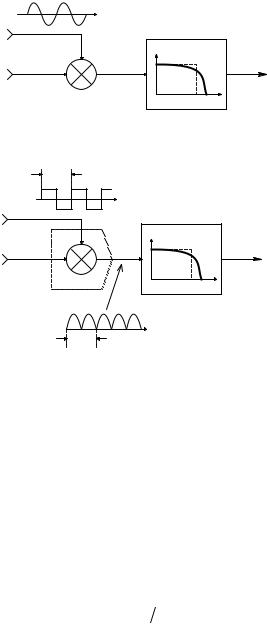
9.8.6Calculation of the SNR Improvement Using a Lock-In Amplifier
A lock-in amplifier (LIA) is used to measure coherent signals, generally at audio frequencies, that are “buried in noise.” More precisely, the input signal- to-noise ratio is very low, often as low as –60 dB. There are two basic architectures used for LIAs. One uses an analog multiplier for signal detection followed by a low-pass filter; this system is shown in Figure 9.20(A). A second LIA architecture, shown in Figure 9.20(B), uses a synchronous rectifier followed by a low-pass filter to measure the amplitude of a coherent signal of constant frequency that is present in an overwhelming amount of noise.
© 2004 by CRC Press LLC
368 |
Analysis and Application of Analog Electronic Circuits |
A |
|
|
vs |
|
LPF |
y |
1 |
vo |
|
||
s1 + n1 |
|
|
AM |
0 0 |
f |
Bout |
||
|
|
A |
T
+1 |
−1 |
vs
s1 + n1
PSR
s1
|
|
LPF |
|
0 0 |
f |
|
Bout |
|
y |
1 |
vo |
|
||
|
|
B |
T
FIGURE 9.20
(A) Basic model for synchronous detection by a lock-in amplifier. A sinusoidal sync. signal is used with an ideal analog multiplier and a low-pass filter. (B) Lock-in operation when the sinusoidal signal to be detected, s1, is effectively multiplied by a ±1 sync signal with the same frequency and phase as s1. Note that s1 is effectively full-wave rectified by the multiplication, but n1 is not.
Assume the input to the LIA is
x(t) = ni(t) + Vs cos(ωo t) |
(9.113) |
and that the noise is zero-mean Gaussian white noise with one-sided power density spectrum, Sn(f ) = η MSV/Hz. The MS input SNR is:
SNR |
|
= |
V2 |
2 |
(9.114) |
|
|
s |
|
||||
in |
ηBin |
|||||
|
|
|
||||
|
|
|
|
|||
where Bin is the Hertz bandwidth over which the input noise is measured.
In the analog multiplier form of the LIA, x(t) is multiplied by an in-phase sync signal, vs(t) = A cos(ωo t). The multiplier output is thus:
© 2004 by CRC Press LLC
Noise and the Design of Low-Noise Amplifiers for Biomedical Applications |
369 |
|||||
y = vs (ni |
+ si ) = A cos(ωot)[ni (t) + Vs cos(ωot)] |
|
||||
= An(t)cos(ωot)+ AVs cos2 (ωot) |
] |
(9.115) |
||||
i |
o |
s |
[ |
o |
|
|
y(t) = An (t)cos(ω |
t)+ (AV |
2) 1 |
+ cos(2ω |
t) |
|
|
Note that the one-sided power spectrum of the first term in Equation 9.115 is the noise PDS shifted up to be centered at ω = ωo. Because Sn(f ) is white, shifting the center of Sn(f ) from 0 to fo = ωo/2π does not change the noise output of the LIA’s output band-pass filter. Thus, the MS output noise voltage from the LIA is von2 = A2 η(1/4τ) MSV, where (1/4τ) can be shown to be the equivalent noise Hertz bandwidth of the simple output R–C low-pass filter, and τ is the output LPF’s time constant. The output LPF removes the 2ωo frequency term in the right-hand term of Equation 9.115, leaving a dc output proportional to the peak value of the sinusoidal signal. Clearly, vos = AVs/2. Thus, the MS SNR at the LIA output is:
SNRout = |
A2 V2 |
4 |
2 |
τ η |
|
s |
|
|
|||
A2η(1 4τ) |
= Vs |
(9.116) |
|||
The noise figure, F, is defined as the ratio of SNRin to SNRout. For an amplifier, F should be as small as possible. In a noise-free amplifier (the limiting case), F = 1. It is easy to show that F for this kind of LIA is:
FLIA = Bout/Bin |
(9.117) |
where Bout = 1/4τ is the Hertz noise bandwidth of the LIA’s output LPF and Bin is the Hertz noise bandwidth over which the input noise is measured. Because the LIA’s desired output is a dc signal proportional to the peak sinusoidal input signal, Bout can be on the order of single Hertz and FLIA can be 1.
In the second model for LIA noise, consider the synchronous rectifier LIA architecture of Figure 9.20(B). Now the sinusoidal signal is full-wave rectified by passing it through an absolute value function that models the synchronous rectifier. The full-wave rectified sinusoidal input signal can be shown to have the Fourier series (Aseltine, 1958):
y(t) = |
s |
(t) |
s |
(2 |
[ |
o |
o |
] |
|
v |
= V |
π) 1 |
− (2 3)cos(2ω |
t)− (2 15)cos(4ω |
t)−≡ |
(9.118) |
|||
Clearly, the average or dc value of y is Vs (2/π).
Curiously, the zero-mean white noise is not conditioned by the absval function of the synchronous rectifier. This is because the synchronous rectifier
© 2004 by CRC Press LLC

370 |
Analysis and Application of Analog Electronic Circuits |
is really created by effectively multiplying x(t) = ni (t) + Vs cos(ωot) by an
even ±1 square wave having the same frequency as, and in phase with, Vs cos(ωo t). This square wave can be represented by the Fourier series:
• |
|
SQWV(t) = an cos(nωot) |
(9.119) |
n=1
where ωo = 2π/T and
T 2
2
an = (2 T) f(t)cos(nωot)dt = (4
 nπ)sin(nπ
 2) [nonzero for n odd] (9.120)
−T 2
2
For a unit cosine (even) square wave that can be written in expanded form,
SQWV(t) =
(9.121)
(4 π)[cos(ωot)− (1 3)cos(3ωot)+ (1 5)cos(5ωot)− (1 7)cos(7ωot)+≡]
The input Gaussian noise is multiplied by SQWV(t):
yn (t) = n(t) ∞ (4 π)
π)
(9.122)
[cos(ωot)− (1 3)cos(3ωot)+ (1 5)cos(5ωot)− (1 7)cos(7ωot)+≡]
Before passing through the LIA’s output LPF, the white one-sided noise power density spectrum can be shown to be:
Sn (f ) = η(4 π)2 [1− (1 3)+ (1 5)− (1 7)+ (1 9)− (1 11)+ (1 13)−≡]2 (9.123) = η MSV
 Hz
Hz
This white noise is conditioned by the output LPF, so the output MS SNR is:
|
|
= |
Vs2 |
(2 π)2 |
|
SNR |
out |
|
|
(9.124) |
|
|
|
||||
|
|
ηBout |
|||
|
|
|
|||
The MS SNR at the input to the LIA is:
SNR |
|
= |
V2 |
2 |
(9.125) |
|
|
s |
|
||||
in |
ηBin |
|||||
|
|
|
||||
|
|
|
|
|||
© 2004 by CRC Press LLC