

- •Analysis and Application of Analog Electronic Circuits to Biomedical Instrumentation
- •Dedication
- •Preface
- •Reader Background
- •Rationale
- •Description of the Chapters
- •Features
- •The Author
- •Table of Contents
- •1.1 Introduction
- •1.2 Sources of Endogenous Bioelectric Signals
- •1.3 Nerve Action Potentials
- •1.4 Muscle Action Potentials
- •1.4.1 Introduction
- •1.4.2 The Origin of EMGs
- •1.5 The Electrocardiogram
- •1.5.1 Introduction
- •1.6 Other Biopotentials
- •1.6.1 Introduction
- •1.6.2 EEGs
- •1.6.3 Other Body Surface Potentials
- •1.7 Discussion
- •1.8 Electrical Properties of Bioelectrodes
- •1.9 Exogenous Bioelectric Signals
- •1.10 Chapter Summary
- •2.1 Introduction
- •2.2.1 Introduction
- •2.2.4 Schottky Diodes
- •2.3.1 Introduction
- •2.4.1 Introduction
- •2.5.1 Introduction
- •2.5.5 Broadbanding Strategies
- •2.6 Photons, Photodiodes, Photoconductors, LEDs, and Laser Diodes
- •2.6.1 Introduction
- •2.6.2 PIN Photodiodes
- •2.6.3 Avalanche Photodiodes
- •2.6.4 Signal Conditioning Circuits for Photodiodes
- •2.6.5 Photoconductors
- •2.6.6 LEDs
- •2.6.7 Laser Diodes
- •2.7 Chapter Summary
- •Home Problems
- •3.1 Introduction
- •3.2 DA Circuit Architecture
- •3.4 CM and DM Gain of Simple DA Stages at High Frequencies
- •3.4.1 Introduction
- •3.5 Input Resistance of Simple Transistor DAs
- •3.7 How Op Amps Can Be Used To Make DAs for Medical Applications
- •3.7.1 Introduction
- •3.8 Chapter Summary
- •Home Problems
- •4.1 Introduction
- •4.3 Some Effects of Negative Voltage Feedback
- •4.3.1 Reduction of Output Resistance
- •4.3.2 Reduction of Total Harmonic Distortion
- •4.3.4 Decrease in Gain Sensitivity
- •4.4 Effects of Negative Current Feedback
- •4.5 Positive Voltage Feedback
- •4.5.1 Introduction
- •4.6 Chapter Summary
- •Home Problems
- •5.1 Introduction
- •5.2.1 Introduction
- •5.2.2 Bode Plots
- •5.5.1 Introduction
- •5.5.3 The Wien Bridge Oscillator
- •5.6 Chapter Summary
- •Home Problems
- •6.1 Ideal Op Amps
- •6.1.1 Introduction
- •6.1.2 Properties of Ideal OP Amps
- •6.1.3 Some Examples of OP Amp Circuits Analyzed Using IOAs
- •6.2 Practical Op Amps
- •6.2.1 Introduction
- •6.2.2 Functional Categories of Real Op Amps
- •6.3.1 The GBWP of an Inverting Summer
- •6.4.3 Limitations of CFOAs
- •6.5 Voltage Comparators
- •6.5.1 Introduction
- •6.5.2. Applications of Voltage Comparators
- •6.5.3 Discussion
- •6.6 Some Applications of Op Amps in Biomedicine
- •6.6.1 Introduction
- •6.6.2 Analog Integrators and Differentiators
- •6.7 Chapter Summary
- •Home Problems
- •7.1 Introduction
- •7.2 Types of Analog Active Filters
- •7.2.1 Introduction
- •7.2.3 Biquad Active Filters
- •7.2.4 Generalized Impedance Converter AFs
- •7.3 Electronically Tunable AFs
- •7.3.1 Introduction
- •7.3.3 Use of Digitally Controlled Potentiometers To Tune a Sallen and Key LPF
- •7.5 Chapter Summary
- •7.5.1 Active Filters
- •7.5.2 Choice of AF Components
- •Home Problems
- •8.1 Introduction
- •8.2 Instrumentation Amps
- •8.3 Medical Isolation Amps
- •8.3.1 Introduction
- •8.3.3 A Prototype Magnetic IsoA
- •8.4.1 Introduction
- •8.6 Chapter Summary
- •9.1 Introduction
- •9.2 Descriptors of Random Noise in Biomedical Measurement Systems
- •9.2.1 Introduction
- •9.2.2 The Probability Density Function
- •9.2.3 The Power Density Spectrum
- •9.2.4 Sources of Random Noise in Signal Conditioning Systems
- •9.2.4.1 Noise from Resistors
- •9.2.4.3 Noise in JFETs
- •9.2.4.4 Noise in BJTs
- •9.3 Propagation of Noise through LTI Filters
- •9.4.2 Spot Noise Factor and Figure
- •9.5.1 Introduction
- •9.6.1 Introduction
- •9.7 Effect of Feedback on Noise
- •9.7.1 Introduction
- •9.8.1 Introduction
- •9.8.2 Calculation of the Minimum Resolvable AC Input Voltage to a Noisy Op Amp
- •9.8.5.1 Introduction
- •9.8.5.2 Bridge Sensitivity Calculations
- •9.8.7.1 Introduction
- •9.8.7.2 Analysis of SNR Improvement by Averaging
- •9.8.7.3 Discussion
- •9.10.1 Introduction
- •9.11 Chapter Summary
- •Home Problems
- •10.1 Introduction
- •10.2 Aliasing and the Sampling Theorem
- •10.2.1 Introduction
- •10.2.2 The Sampling Theorem
- •10.3 Digital-to-Analog Converters (DACs)
- •10.3.1 Introduction
- •10.3.2 DAC Designs
- •10.3.3 Static and Dynamic Characteristics of DACs
- •10.4 Hold Circuits
- •10.5 Analog-to-Digital Converters (ADCs)
- •10.5.1 Introduction
- •10.5.2 The Tracking (Servo) ADC
- •10.5.3 The Successive Approximation ADC
- •10.5.4 Integrating Converters
- •10.5.5 Flash Converters
- •10.6 Quantization Noise
- •10.7 Chapter Summary
- •Home Problems
- •11.1 Introduction
- •11.2 Modulation of a Sinusoidal Carrier Viewed in the Frequency Domain
- •11.3 Implementation of AM
- •11.3.1 Introduction
- •11.3.2 Some Amplitude Modulation Circuits
- •11.4 Generation of Phase and Frequency Modulation
- •11.4.1 Introduction
- •11.4.3 Integral Pulse Frequency Modulation as a Means of Frequency Modulation
- •11.5 Demodulation of Modulated Sinusoidal Carriers
- •11.5.1 Introduction
- •11.5.2 Detection of AM
- •11.5.3 Detection of FM Signals
- •11.5.4 Demodulation of DSBSCM Signals
- •11.6 Modulation and Demodulation of Digital Carriers
- •11.6.1 Introduction
- •11.6.2 Delta Modulation
- •11.7 Chapter Summary
- •Home Problems
- •12.1 Introduction
- •12.2.1 Introduction
- •12.2.2 The Analog Multiplier/LPF PSR
- •12.2.3 The Switched Op Amp PSR
- •12.2.4 The Chopper PSR
- •12.2.5 The Balanced Diode Bridge PSR
- •12.3 Phase Detectors
- •12.3.1 Introduction
- •12.3.2 The Analog Multiplier Phase Detector
- •12.3.3 Digital Phase Detectors
- •12.4 Voltage and Current-Controlled Oscillators
- •12.4.1 Introduction
- •12.4.2 An Analog VCO
- •12.4.3 Switched Integrating Capacitor VCOs
- •12.4.6 Summary
- •12.5 Phase-Locked Loops
- •12.5.1 Introduction
- •12.5.2 PLL Components
- •12.5.3 PLL Applications in Biomedicine
- •12.5.4 Discussion
- •12.6 True RMS Converters
- •12.6.1 Introduction
- •12.6.2 True RMS Circuits
- •12.7 IC Thermometers
- •12.7.1 Introduction
- •12.7.2 IC Temperature Transducers
- •12.8 Instrumentation Systems
- •12.8.1 Introduction
- •12.8.5 Respiratory Acoustic Impedance Measurement System
- •12.9 Chapter Summary
- •References

414 |
|
|
Analysis and Application of Analog Electronic Circuits |
|||
|
|
|
|
|
|
S2 |
|
|
|
|
S1 |
|
+5 V |
|
R |
|
R/2 |
|
V1 |
|
|
|
|
C |
|||
|
|
|
|
|
|
|
|
R |
|
R |
|
|
|
|
|
|
|
|
|
V2 |
VR |
Vx |
|
OA-1 |
|
|
OA-2 |
|
|
|
|
|
|
|
|
|
|
|
|
|
Comp. |
|
|
RST |
|
|
|
Q |
|
N-bit |
|
Control |
|
|
|
|
|
|
|
|
||
|
counter CP |
|
logic |
|
|
|
|
|
|
EN |
CP |
|
|
EOC Convert
Offset binary output
Clock
FIGURE 10.16
Block diagram of a bipolar-input dual-slope integrating ADC. The output is in offset binary code.
|
|
|
|
2N T |
|
|
[Vx ]2N Tc |
|
|
|
|
|
|
|
c |
VR 2N Tc |
|
|
|
V2 (2 |
N |
Tc ) = |
1 |
(VR + [Vx ])dt = |
+ |
(10.41) |
|||
|
2RC |
2RC |
2RC |
||||||
|
|
|
|
0 |
|
|
|
|
|
The number of clock cycles required to integrate V2 (2N Tc) to zero is M:
|
VR 2N Tc |
+ |
[Vx ]2N Tc |
− |
VR MTc |
= 0 |
(10.42) |
||
|
2RC |
|
|
||||||
|
|
2RC |
|
|
|
RC |
|
||
Solving for M: |
|
|
|
|
|
|
|
|
|
|
M = 2N−1 (1 |
+ [Vx ] |
VR ) |
(10.43) |
|||||
Note that when [Vx] = −VR, M = 0, when [Vx] = 0, M = 2N−1 (1 MSB), and when [Vx] = +VR, M = 2N, giving a true offset binary output code. Note that this dual-slope integrating ADC also has accuracy independent of RC and Tc.
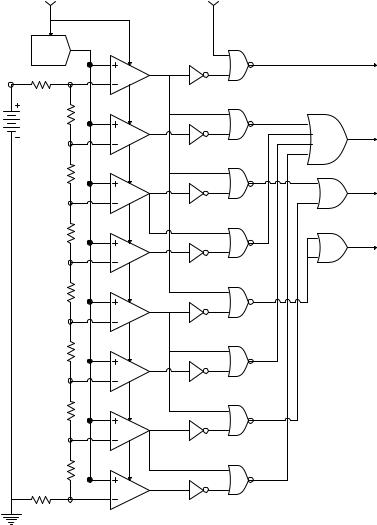
10.5.5Flash Converters
The fastest ADCs are flash converters (FADCs) that enable signal sampling in the ns range and thus are widely used in medical ultrasound systems,
© 2004 by CRC Press LLC
Digital Interfaces |
415 |
S |
EXP |
Vx  T & H
T & H
STB
R/2 7.5VR /8 |
C1 |
R
VR
C2
6.5VR /8
R
C3
5.5VR /8
R
C4
4.5VR /8
R
C5
3.5VR /8
R
C6
2.5VR /8
R
C7
1.5VR /8
R
R/2 |
C8 |
0.5VR /8
FIGURE 10.17
A 3-bit flash ADC.
Overrange
output
(LSB)
Bit 3
Bit 2
(MSB)
Bit 1
sonar and radar data conversion, and certain communications applications. Data conversion rates into the hundreds of MSa/sec are typical. Figure 10.17 illustrates an N = 3-bit flash ADC with straight binary output. 2N − 1 = 7 voltage comparators are used for conversion; comparator C1 is used to signal over-range. Thus, an 8-bit FADC uses 255 analog comparators, plus one for over-range. Figure 10.18 illustrates the transfer characteristic of the 3-bit FADC. The Analog Devices AD770 8-bit FADC uses three blocks of 64 comparators and one block of 65 comparators and two levels of bit decoding to
© 2004 by CRC Press LLC
416 |
Analysis and Application of Analog Electronic Circuits |
O.R. = HI
{bk} |
3-bit binary |
|
|
|
|
|
|
|
|
output code |
|
|
|
|
|
|
|
||
|
|
|
|
|
|
|
|
||
111 |
|
|
|
|
|
∞ resolution |
|
|
|
|
|
|
|
|
|
|
|
|
|
|
|
|
|
|
|
line |
|
|
|
110 |
|
|
|
|
|
|
|
|
|
|
|
1 LSB |
|
|
|
|
|
|
|
101 |
|
|
|
|
|
|
|
|
|
100 |
|
|
|
|
|
|
|
|
|
011 |
|
|
|
|
|
|
|
|
|
010 |
|
|
|
|
|
|
|
|
|
001 |
|
|
|
|
|
|
|
|
|
000 |
|
|
|
|
|
|
|
|
|
0.000 |
0.125 |
0.250 |
0.375 |
0.500 |
0.625 |
0.750 |
0.875 |
1.000 |
|
|
|
|
|
|
[vx]/VR |
|
0.9375 |
|
|
|
|
|
|
(Normalized input voltage) |
|
|
|||
|
|
|
|
|
([vx] =7.5VR /8) |
|
|||
FIGURE 10.18
Transfer characteristic of an ideal 3-bit flash ADC.
obtain an 8-bit ECL-compatible, binary output with a guaranteed 200 MSa/sec rate.
One of the problems in realizing an 8-bit FADC is keeping the dc offset voltages of the 256 comparators small, with low, equal tempcos, and also keeping the resistors matched in the 2N-resistor voltage divider. To realize flash conversions with resolutions greater than 8 bits, a two-step architecture can be used, as shown in Figure 10.19. For example, a 12-bit FADC can be made by letting K = M = 6 bits; thus, each subconverter needs only 26 = 64 comparators. Assuming unipolar operation, 0 ≤ vx ≤ VFS. The output of the K-MSB DAC following a conversion of [vx(nT)] is:
K |
|
V1 = VFS bi 2i |
(10.44) |
i =1
The input to the M-lesser bits T and H and FADC is:
© 2004 by CRC Press LLC
Digital Interfaces |
|
|
|
|
|
|
|
|
417 |
|||||
|
|
|
[vx (nT)] |
+ |
|
|
|
Ve |
||||||
vx(t) |
T & H 1 |
|
|
|
|
|
|
|
|
|
Kv = 2K |
|
|
|
|
|
|
|
|
|
|
|
|
|
|
V2 |
|||
|
|
|
|
|
|
|
|
|
|
|
|
|
|
|
|
|
|
|
|
|
|
− |
|
|
|
|
|
||
|
|
|
|
|
|
|
|
|
|
|
|
|
T & H 2 |
|
|
Conversion |
|
|
|
|
V1 |
|
|
|
|
|
[V2] |
||
|
|
|
|
|
|
|
|
|
|
|||||
|
clock |
|
|
|
|
|
|
|
|
|
||||
|
|
|
|
|
|
|
|
|
|
|
|
|
||
|
|
|
|
|
|
|
|
|
|
|
|
|
||
|
|
|
K-bit FADC |
|
|
|
K-bit |
|
|
M-bit |
||||
|
|
|
|
|
|
|
||||||||
|
|
|
|
|
|
DAC |
|
|
FADC |
|||||
|
|
|
|
|
|
|
|
|
||||||
|
|
|
K most |
|
|
|
|
|
M less |
|||||
|
|
|
significant bits |
|
|
|
|
|
significant bits |
|||||
M + K = N-bit output
FIGURE 10.19
Architecture of a two-step flash ADC. This design is more efficient when N ≥ 8 is desired.
|
|
[ |
|
(nT) |
− V |
K |
ˆ |
|
V = 2K |
v |
b |
2i ˜ |
(10.45) |
||||
2 |
|
x |
] |
FS i |
˜ |
|
||
|
|
|
|
|
|
i =1 |
↓ |
|
The voltage difference in parentheses is Ve. Thus, the second FADC generates a binary code on the quantized remnant, Ve, to give a net N = (K + M)-bit output. Because the K- and M-bit FADCs use (2K − 1) and (2M − 1) comparators respectively, the system is generally less expensive and easier to build than a single N-bit FADC. The total coded output of the system is:
|
|
(nT) |
= V |
|
K |
M |
|
|
ˆ |
= V |
N |
|
[ |
v |
|
b 2i + |
|
b |
|
2j ˜ |
b 2k |
(10.46) |
|||
x |
] |
FS |
i |
|
j |
˜ |
FS k |
|
||||
|
|
|
|
|
i =1 |
j =1 |
|
|
↓ |
|
k =1 |
|
When flash converters that sample at over 100 MSa/sec are used, special attention must be paid to how the digital data are handled. High-speed logic (e.g., ECL) must be used and data must be stored temporarily in shift registers and high-speed RAM before permanent recording can take place on a magnetic hard disk or optical disk. FADCs also are greedy for die size and operating power. For every bit increase in FADC resolution, the size of the ADC core circuitry (comparators, resistors, decoding logic) essentially doubles, as does the chip’s power dissipation (Maxim, 2001). Conversion time, however, is independent of the bit resolution, N, and is fast; the state of the art for 2- and 4-bit FADCs is a sample rate of about 1 GSa/sec.
© 2004 by CRC Press LLC
418 |
|
Analysis and Application of Analog Electronic Circuits |
|||||||||||||||||
|
|
+VR |
|
|
|
|
|
|
|
|
|
|
|
|
|
|
|
|
|
|
|
|
|
|
|
|
|
|
|
|
|
|
|
|
|
|
|
|
|
|
|
SPDT |
|
|
|
|
|
|
|
|
|
|
|
|
|
|
|
|
|
|
|
MOS Switch |
|
|
|
|
|
|
|
|
|
|
|
|
|
||||
|
|
−VR |
|
|
|
|
|
|
|
|
|
|
|
|
|
|
|
|
|
|
|
|
|
|
|
|
|
|
|
|
|
|
|
|
|
|
|
|
|
|
R |
C |
|
|
|
“1-bit ADC” |
|
|
|
|
|
|
|
|
|
||||
Vs |
|
|
|
|
|
|
|
|
|
|
|
|
|
|
|||||
R |
|
|
|
|
|
|
|
|
|
|
|
|
|
|
|
|
|
|
|
|
|
|
|
|
|
|
|
|
|
|
|
|
|
|
|
|
|
|
|
|
|
|
|
|
|
|
|
|
|
|
|
|
|
|
|
|
|
||
Vx |
|
V1 |
|
|
|
|
|
|
|
|
|
|
|
|
|
||||
|
|
OA |
|
D Flip-flop |
|
|
|
|
|
|
|
||||||||
|
|
|
|
Comp. |
|
|
|
D |
Q |
|
|
|
|
|
|
|
Output |
||
|
|
|
|
|
|
|
|
|
|
|
|
|
|
|
|||||
|
|
|
|
|
|
V2 |
|
|
|
|
|
|
|
|
Digital |
||||
|
|
|
|
|
|
|
|
|
|
|
|
|
|
|
|
|
|||
|
|
|
|
|
|
|
|
|
|
|
_ |
|
|
|
|
|
filter & |
|
|
|
|
|
|
|
|
|
|
|
|
|
|
|
|
|
|
decimator |
N bits |
||
|
|
|
|
|
|
|
|
|
|
CP |
Q |
|
|
|
|
|
|||
|
|
|
|
|
|
|
|
|
|
|
|
|
|
|
|
|
|||
|
|
|
|
|
|
|
|
|
|
|
|
|
|
|
|
|
|
|
@ fo << fc |
|
|
|
|
|
|
|
|
|
|
|
|
|
|
|
|
|
|
|
|
|
|
|
Clock |
|
fc |
|
÷ K |
|
|
|
fo |
|
|
||||||
|
|
|
|
|
|
|
|
|
|
|
|
|
|
|
|
||||
|
|
∆- Modulator |
|
|
|
|
|
|
|
|
|
|
|
|
|
||||
|
|
|
|
|
|
|
|
|
|
|
|
|
|
|
|||||
FIGURE 10.20 |
|
|
|
|
|
|
|
|
– modulator is in the dotted box. |
||||||||||
Block diagram of a first-order, delta–sigma ADC. The |
|||||||||||||||||||
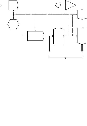
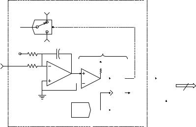
10.5.6Delta–Sigma ADCs
Delta–sigma ADCs are also called oversampled or noise-shaping converters. Oversampling ADCs are based on the principle of being able to trade off accuracy in time for accuracy in amplitude. Figure 10.20 illustrates the circuit of a first -order – ADC. The circuit in the box is a first-order – modulator. The digital filter and decimator produces the N-bit, digital output.
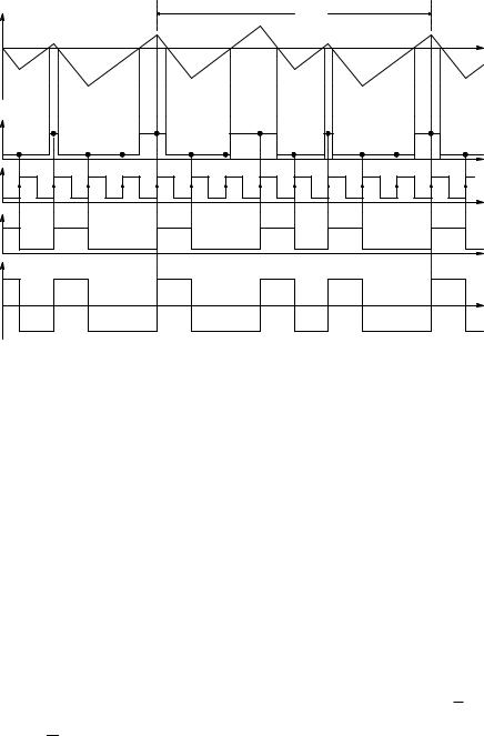
First, the operation of the – modulator in the time domain will be analyzed. Set Vx 0 and let the MOS switch apply −VR to the integrator so that its output, V1, goes positive. The comparator output, V2, applied to the D input of the D flip-flop (DFF) will be HI. At the rising edge of the next clock pulse, HI is seen at the Q output of the DFF. This HI causes the MOS switch to switch the integrator input to +VR, so the integrator output V1 begins to ramp down. When V1 goes negative, the comparator output V2 goes LO. Again when the clock pulse goes HI, the LO at D is sent to the DFF Q output. This LO again sets the MOS switch to −VR, causing V2 to ramp
positively until it goes positive, setting V2 HI, etc.
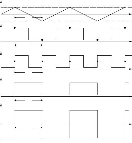
Figure 10.21 shows the – modulator’s waveforms for Vx = 0. Q is the DFF output, which is the comparator output, V2, latched in when the CP goes high. The peak-to-peak height of the steady-state triangle wave oscillation seen at V1 can easily be shown to be equal to:
2V |
= |
VRTc |
(10.47) |
|
|||
1m |
|
RC |
|
|
|
|
© 2004 by CRC Press LLC
Digital Interfaces |
419 |
V1 |
V1m |
t |
0 |
Tc |
−V1m |
V2 |
t |
0 |
Tc |
CP |
t |
0 |
Tc |
Q |
t |
0 |
Tc |
Vs |
+VR |
t |
0 |
Tc |
−VR |
FIGURE 10.21
Waveforms in a first-order – modulator when Vx = 0.
where Tc is the DSDAC’s clock period and the other parameters are given in the figure. The average value of Vs = 0.
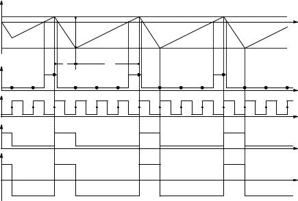
Now set Vx = +VR/4 and examine the – ADC’s waveforms (refer to Figure 10.22). Let the system start with V1 = 0 at t = 0 and begin to integrate Vx and Vs = +VR. Initially, the integrator output V1 ramps negative as v1(t) = −[5VR/(4RC)] t. At the first positive-going clock wave, the LO comparator output, V2, is latched to the DFF’s Q output, setting it low. When Q goes low, the MOS switch makes Vs = −VR. Now the integrator output ramps upward with slope +3VR/(4RC). When V1 goes positive, the second positive clock transition latches the HI V2 to Q, setting Vs to +VR. Now the integrator output, V1, ramps down again with slope −5VR/(4RC).
© 2004 by CRC Press LLC
420 |
Analysis and Application of Analog Electronic Circuits |
T1 = 8Tc |
V1 |
t |
0 |
HI |
V2 |
LO |
|
HI |
CP |
|
|
LO |
|
Q |
HI |
LO |
Vs |
VR |
0 |
−VR |
FIGURE 10.22
Waveforms in a first-order – modulator when Vx = +VR /4.
When V1 < 0, V2 goes LO. The third positive clock transition latches this LO to the Q output of the DFF. As before, this sets Vs to −VR, the integrator output again ramps positive, and the cycle repeats, etc. Note that there is a steady-state (SS) oscillation in V1, V2, Q, and Vs with a period of eight clock periods. The SS duty cycle of Q is 37.5%, and Vs = −¼.
It is also of interest to examine the – ADC’s waveforms when Vx = +VR/2. Now let the system start with V1 = 0 at t = 0 and begin to integrate Vx with Vs = +VR. Assuming Vx is constant, V1 ramps negative as v1(t) = −3VR t/(2RC), causing the comparator output, V2, to be LO. At the first positivegoing clock pulse, the DFF latches the low D input to Q, causing the MOS switch to make Vs = −VR. Now the net input to the integrator is
–VR/2 and the integrator output begins to go positive with slope +VR/(2RC), as shown in Figure 10.23. When V1 first goes positive, V2 goes HI. At the third clock HI transition, the DFF output goes HI, setting the MOS switch to −VR. Now the net input to the integrator is +3VR/2, V1 begins to ramp down again with slope −3VR/(2RC), and the ADC process repeats itself indefinitely until Vx changes. From the waveforms in this figure
where Vx = VR/2, it can be seen that the duty cycle of Q is 25% and Vs =
–½. From the three sets of Vs waveforms, it can be seen that, in general,
Vx = −VR Vs .
Now consider the operation of first-order – ADC. If the number of ones in the output data stream (i.e., the DFF’s Q output) is counted over a sufficient number of samples (clock cycles), the counter’s digital output
© 2004 by CRC Press LLC
Digital Interfaces |
421 |
|
|
V1 |
|
|
|
t |
0 |
|
|
|
|
3VRTc /(2RC) |
|
Tc |
3Tc |
HI |
V2 |
|
|
|
|
LO |
|
|
HI |
CP |
|
|
LO |
|
Q |
HI |
LO |
Vs |
VR |
0 |
−VR |
FIGURE 10.23
Waveforms in a first-order – modulator when Vx = +VR /2.
will represent the digital value of the analog input, Vx. Obviously, this method of averaging will only work for DC or low-frequency Vx. In addition, at least 2N clock cycles must be counted in order to obtain N-bit effective resolution. In the – ADC, the modulator’s DFF Q output is the input to the block labeled “digital filter and decimator.” The digital low-pass filter precedes the decimator and serves two functions: (1) it acts as an anti-aliasing filter for the final sampling rate, fo, and (2) it filters out the higher frequency noise produced by the – modulator.
According to Analog Devices’ AN-283 (Sigma–Delta ADCs and DACs):
The final data rate reduction is performed by digitally resampling the filtered output using a process called decimation. The decimation of a discrete-time signal is shown in Figure …, where the sampling rate of the input signal x(n) is at a rate which is to be reduced by a factor of 4. The signal is resampled at the lower rate (the decimation rate), s(n) [ fo]. Decimation can also be viewed as the method by which the redundant signal information introduced by the oversampling process is removed.
In sigma–delta ADCs it is quite common to combine the decimation function with the digital filtering function. This results in an increase in computational efficiency if done correctly.
Figure 10.24 illustrates a heuristic frequency-domain block diagram approximation for a first-order – ADC. To appreciate what happens in the system in the frequency domain, find the transfer function for the analog
© 2004 by CRC Press LLC