

- •Analysis and Application of Analog Electronic Circuits to Biomedical Instrumentation
- •Dedication
- •Preface
- •Reader Background
- •Rationale
- •Description of the Chapters
- •Features
- •The Author
- •Table of Contents
- •1.1 Introduction
- •1.2 Sources of Endogenous Bioelectric Signals
- •1.3 Nerve Action Potentials
- •1.4 Muscle Action Potentials
- •1.4.1 Introduction
- •1.4.2 The Origin of EMGs
- •1.5 The Electrocardiogram
- •1.5.1 Introduction
- •1.6 Other Biopotentials
- •1.6.1 Introduction
- •1.6.2 EEGs
- •1.6.3 Other Body Surface Potentials
- •1.7 Discussion
- •1.8 Electrical Properties of Bioelectrodes
- •1.9 Exogenous Bioelectric Signals
- •1.10 Chapter Summary
- •2.1 Introduction
- •2.2.1 Introduction
- •2.2.4 Schottky Diodes
- •2.3.1 Introduction
- •2.4.1 Introduction
- •2.5.1 Introduction
- •2.5.5 Broadbanding Strategies
- •2.6 Photons, Photodiodes, Photoconductors, LEDs, and Laser Diodes
- •2.6.1 Introduction
- •2.6.2 PIN Photodiodes
- •2.6.3 Avalanche Photodiodes
- •2.6.4 Signal Conditioning Circuits for Photodiodes
- •2.6.5 Photoconductors
- •2.6.6 LEDs
- •2.6.7 Laser Diodes
- •2.7 Chapter Summary
- •Home Problems
- •3.1 Introduction
- •3.2 DA Circuit Architecture
- •3.4 CM and DM Gain of Simple DA Stages at High Frequencies
- •3.4.1 Introduction
- •3.5 Input Resistance of Simple Transistor DAs
- •3.7 How Op Amps Can Be Used To Make DAs for Medical Applications
- •3.7.1 Introduction
- •3.8 Chapter Summary
- •Home Problems
- •4.1 Introduction
- •4.3 Some Effects of Negative Voltage Feedback
- •4.3.1 Reduction of Output Resistance
- •4.3.2 Reduction of Total Harmonic Distortion
- •4.3.4 Decrease in Gain Sensitivity
- •4.4 Effects of Negative Current Feedback
- •4.5 Positive Voltage Feedback
- •4.5.1 Introduction
- •4.6 Chapter Summary
- •Home Problems
- •5.1 Introduction
- •5.2.1 Introduction
- •5.2.2 Bode Plots
- •5.5.1 Introduction
- •5.5.3 The Wien Bridge Oscillator
- •5.6 Chapter Summary
- •Home Problems
- •6.1 Ideal Op Amps
- •6.1.1 Introduction
- •6.1.2 Properties of Ideal OP Amps
- •6.1.3 Some Examples of OP Amp Circuits Analyzed Using IOAs
- •6.2 Practical Op Amps
- •6.2.1 Introduction
- •6.2.2 Functional Categories of Real Op Amps
- •6.3.1 The GBWP of an Inverting Summer
- •6.4.3 Limitations of CFOAs
- •6.5 Voltage Comparators
- •6.5.1 Introduction
- •6.5.2. Applications of Voltage Comparators
- •6.5.3 Discussion
- •6.6 Some Applications of Op Amps in Biomedicine
- •6.6.1 Introduction
- •6.6.2 Analog Integrators and Differentiators
- •6.7 Chapter Summary
- •Home Problems
- •7.1 Introduction
- •7.2 Types of Analog Active Filters
- •7.2.1 Introduction
- •7.2.3 Biquad Active Filters
- •7.2.4 Generalized Impedance Converter AFs
- •7.3 Electronically Tunable AFs
- •7.3.1 Introduction
- •7.3.3 Use of Digitally Controlled Potentiometers To Tune a Sallen and Key LPF
- •7.5 Chapter Summary
- •7.5.1 Active Filters
- •7.5.2 Choice of AF Components
- •Home Problems
- •8.1 Introduction
- •8.2 Instrumentation Amps
- •8.3 Medical Isolation Amps
- •8.3.1 Introduction
- •8.3.3 A Prototype Magnetic IsoA
- •8.4.1 Introduction
- •8.6 Chapter Summary
- •9.1 Introduction
- •9.2 Descriptors of Random Noise in Biomedical Measurement Systems
- •9.2.1 Introduction
- •9.2.2 The Probability Density Function
- •9.2.3 The Power Density Spectrum
- •9.2.4 Sources of Random Noise in Signal Conditioning Systems
- •9.2.4.1 Noise from Resistors
- •9.2.4.3 Noise in JFETs
- •9.2.4.4 Noise in BJTs
- •9.3 Propagation of Noise through LTI Filters
- •9.4.2 Spot Noise Factor and Figure
- •9.5.1 Introduction
- •9.6.1 Introduction
- •9.7 Effect of Feedback on Noise
- •9.7.1 Introduction
- •9.8.1 Introduction
- •9.8.2 Calculation of the Minimum Resolvable AC Input Voltage to a Noisy Op Amp
- •9.8.5.1 Introduction
- •9.8.5.2 Bridge Sensitivity Calculations
- •9.8.7.1 Introduction
- •9.8.7.2 Analysis of SNR Improvement by Averaging
- •9.8.7.3 Discussion
- •9.10.1 Introduction
- •9.11 Chapter Summary
- •Home Problems
- •10.1 Introduction
- •10.2 Aliasing and the Sampling Theorem
- •10.2.1 Introduction
- •10.2.2 The Sampling Theorem
- •10.3 Digital-to-Analog Converters (DACs)
- •10.3.1 Introduction
- •10.3.2 DAC Designs
- •10.3.3 Static and Dynamic Characteristics of DACs
- •10.4 Hold Circuits
- •10.5 Analog-to-Digital Converters (ADCs)
- •10.5.1 Introduction
- •10.5.2 The Tracking (Servo) ADC
- •10.5.3 The Successive Approximation ADC
- •10.5.4 Integrating Converters
- •10.5.5 Flash Converters
- •10.6 Quantization Noise
- •10.7 Chapter Summary
- •Home Problems
- •11.1 Introduction
- •11.2 Modulation of a Sinusoidal Carrier Viewed in the Frequency Domain
- •11.3 Implementation of AM
- •11.3.1 Introduction
- •11.3.2 Some Amplitude Modulation Circuits
- •11.4 Generation of Phase and Frequency Modulation
- •11.4.1 Introduction
- •11.4.3 Integral Pulse Frequency Modulation as a Means of Frequency Modulation
- •11.5 Demodulation of Modulated Sinusoidal Carriers
- •11.5.1 Introduction
- •11.5.2 Detection of AM
- •11.5.3 Detection of FM Signals
- •11.5.4 Demodulation of DSBSCM Signals
- •11.6 Modulation and Demodulation of Digital Carriers
- •11.6.1 Introduction
- •11.6.2 Delta Modulation
- •11.7 Chapter Summary
- •Home Problems
- •12.1 Introduction
- •12.2.1 Introduction
- •12.2.2 The Analog Multiplier/LPF PSR
- •12.2.3 The Switched Op Amp PSR
- •12.2.4 The Chopper PSR
- •12.2.5 The Balanced Diode Bridge PSR
- •12.3 Phase Detectors
- •12.3.1 Introduction
- •12.3.2 The Analog Multiplier Phase Detector
- •12.3.3 Digital Phase Detectors
- •12.4 Voltage and Current-Controlled Oscillators
- •12.4.1 Introduction
- •12.4.2 An Analog VCO
- •12.4.3 Switched Integrating Capacitor VCOs
- •12.4.6 Summary
- •12.5 Phase-Locked Loops
- •12.5.1 Introduction
- •12.5.2 PLL Components
- •12.5.3 PLL Applications in Biomedicine
- •12.5.4 Discussion
- •12.6 True RMS Converters
- •12.6.1 Introduction
- •12.6.2 True RMS Circuits
- •12.7 IC Thermometers
- •12.7.1 Introduction
- •12.7.2 IC Temperature Transducers
- •12.8 Instrumentation Systems
- •12.8.1 Introduction
- •12.8.5 Respiratory Acoustic Impedance Measurement System
- •12.9 Chapter Summary
- •References
12
Examples of Special Analog Circuits and
Systems in Biomedical Instrumentation
12.1 Introduction
Biomedical engineers may be expected to understand many specialized integrated circuits and be able to incorporate them effectively into biomedical measurement system designs. These integrated circuits include but are not limited to:
•Phase-sensitive rectifiers
•Phase detectors
•Voltageand current-controlled oscillators
•Phase-locked loops
•True-RMS converters
•IC thermometers
Most designers and vendors of analog ICs, such as Analog Devices, Burr–Brown, Maxim, National, etc., make one or more of the preceding ICs. In describing them, this chapter will stress application as well as design.
12.2 The Phase-Sensitive Rectifier
12.2.1Introduction
The phase-sensitive rectifier (PSR) is also known as the phase-sensitive detector, the synchronous rectifier or detector, or the balanced demodulator. Its primary role is to recover the modulating signal in a double-sideband, suppressedcarrier (amplitude) modulated carrier. The PSR is also at the heart of the lock-in amplifier, which is widely used in photonics and in certain applications
467
© 2004 by CRC Press LLC

468 |
Analysis and Application of Analog Electronic Circuits |
in physics to recover a low-frequency modulating signal. A PSR will also demodulate ordinary AM. The four major embodiments of the PSR are the
(1) analog multiplier/low-pass filter (LPF) PSR; (2) switched op amp PSR;
(3) electromechanical chopper PSR; and (4) balanced diode bridge PSR. The analog multiplier PSR will be examined first.
12.2.2The Analog Multiplier/LPF PSR
Just as a DSBSCM carrier can be made by multiplying a sinusoidal carrier by the low-frequency modulating signal, the DSBSCM signal can be demodulated by multiplying the modulated carrier by a carrier frequency reference signal of the correct phase (refer to Figure 11.1B in the preceding chapter). Let the coherent modulating signal be a low-frequency sinusoid:
vm(t) = Vm sin(ωm t) |
(12.1) |
The carrier is: |
|
vc(t) = Vc cos(ωc t) |
(12.2) |
and the modulated carrier is: |
|
ym (t) = (Vm Vc 2){sin[(ωc + ωm )t]+ sin[(ωc − ωm )t]} |
(12.3) |
The reference signal is of the same frequency as the carrier but in general differs in phase by a fixed angle, (π/2 + ϕ) radians. By trigonometric identity, this is:
vr(t) = Vr sin(ωc t + ϕ) |
(12.4) |
The analog multiplier output is:
vz (t) = {vr (t) ym (t)} 10 = (VmVc Vr
  20){cos[ωmt − ϕ]− cos[(2ωc + ωm )t + ϕ]+
cos[ωmt + ϕ]− cos[(2ωc − ωm )t − ϕ]} |
(12.5) |
(Note that the output of a transconductance-type analog multiplier IC is the product of the inputs divided by 10.) The unity-gain low-pass filter removes the two 2ωc terms, leaving (recall that sinθ is an odd function):
|
= (VmVcVr 20){cos[ωmt − ϕ]+ cos[ωmt + ϕ]} |
|
vx (t) |
(12.6) |
© 2004 by CRC Press LLC

Examples of Special Analog Circuits and Systems |
469 |
From the trigonometric identity, {cosα + cosβ} = 2 cos[½(α + β)] cos[½(α − β)]:
|
= (VmVcVr 10)cos(ωmt)cos(ϕ) |
|
vz (t) |
(12.7) |
In the preceding development, it was assumed that 0 < ωm ωb ωc, where ωb is the LPF’s break frequency. Note that the recovered modulating signal is maximum when the reference signal is in phase with the quadrature carrier of the DSBSCM signal. Thus, an analog multiplier can form DSBSCM signals and also demodulate them, returning a signal vm(t).
12.2.3The Switched Op Amp PSR
Figure 11.13 in Chapter 11 illustrates a PSR that uses three op amps and a digitally controlled analog MOS switch to demodulate DSBSCM signals. The MOS switch, when closed, has a very low resistance. When it is open, its resistance is on the order of megohms. The switch is controlled by the function, sgn{Vr sin(ωc t)}, which is +1 when sin(ωc t) is ≥ 0 and −1 when sin(ωc t) < 0. The output, vz(t), is a full-wave rectified ym(t), which goes negative when the sign of the modulating signal, vm(t) goes negative. It is easy to see that after low-pass filtering, vz(t) is vm(t). The average (dc value) of a full-wave rectified sine wave is πVpk/2. Note that the action of the switch effectively multiplies the DSBSCM input signal by a ±1 peak value square wave of frequency ωc/2π Hz.
12.2.4The Chopper PSR
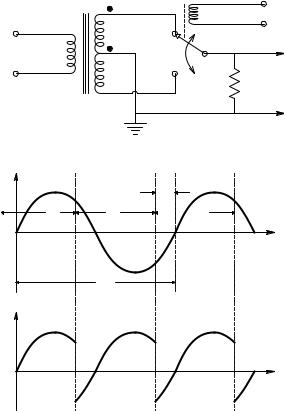
Figure 12.1(A) illustrates the circuit of an electromechanical chopper. Electromechanical choppers are basically SPDT switches commutated by a driver coil at switching frequencies from 50 to 400 Hz or so. Developed in the WWII era as modulator/demodulators for ac DSBSCM signals, they are now obsolete. The same SPDT action can be obtained using appropriately buffered MOS switches that can be commutated in the hundreds of kilohertz or by photoelectrically turning phototransistors on and off in a photoelectric chopper. The basic electromechanical chopper uses a center-tapped signal transformer to couple the DSBSCM carrier to the switch points.
Figure 12.1(B) illustrates the raw switch output, vz(t). This signal must be low-pass filtered to recover vm(t). Note that the phase shift ϕ causes some of the chopped signal to be negative over ϕ radians of the cycle. When averaged, this negative area subtracts from the output signal. It can be shown that the phase error ϕ in the reference signal effectively multiplies the averager output by cos(ϕ). Thus, if the reference signal is 90∞ out of phase, the low-pass filtered output will always be zero.
© 2004 by CRC Press LLC
470 |
Analysis and Application of Analog Electronic Circuits |
|
|
|
vr(t) |
|
|
+ |
|
|
|
p |
|
vm(t) |
|
−n |
+ |
|
|
||
|
|
R |
vz(t) |
|
A |
|
− |
|
|
|
|
vm(t) |
|
|
|
|
|
ϕ |
|
p |
n |
p |
ωt |
0 |
|
|
|
|
|
|
|
|
2π |
|
|
vz(t) |
|
|
|
0 |
|
|
ωt |
|
|
|
|
|
|
B |
|
FIGURE 12.1
(A) Circuit of an electromechanical chopper phase-sensitive rectifier (PSR). (B) Upper waveform: chopper input. p and n denote the intervals the chopper switch dwells on the positive or minus contacts, respectively. Lower waveform: chopper output when the switch control sync voltage, vr(t), is out of phase with vm(t) by ϕ radians. Perfect full-wave rectification is not achieved.
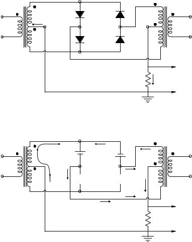
12.2.5The Balanced Diode Bridge PSR
Still another circuit that can be used to demodulate DSBSCM signals is the balanced diode bridge PSR, illustrated in Figure 12.2. The modulated signal, ym(t), and the reference signal, vr(t), are coupled to the diode bridge by two center-tapped transformers. The transformer on the left is called the signal transformer and the one on the right is the reference transformer.
To understand how the diode bridge PSR works, refer to Figure 12.3. Assume vr(t) > 0, diodes a and b conduct current ir+, and c and d are cut off (treated as open circuits). The positive signal voltage at node B causes a current, ima and imb, to flow through diodes a and b, respectively. Assume that ima > ir+, so diode a continues to conduct. The currents ima and imb flow through both halves of the reference transformer secondary, combine, and flow to
© 2004 by CRC Press LLC
Examples of Special Analog Circuits and Systems |
|
|
471 |
||
|
|
B |
|
|
|
|
b |
|
a |
|
|
ym(t) |
im |
|
|
|
vr(t) |
C |
A |
|
|
||
|
c |
|
d |
|
|
|
Signal |
D |
|
|
Reference |
|
|
|
|
||
|
transformer |
|
|
|
transformer |
|
|
|
|
|
+ |
|
|
|
R |
im |
vz(t) |
FIGURE 12.2
A balanced-bridge diode PSR.
B
|
v+d |
|
ir |
|
|
im+ |
b |
vd |
a |
ir |
|
|
|
|
+ |
|
|
ym(t) |
|
C |
A |
ima |
vr(t) |
|
ir |
|
|
|
|
|
|
|
|
|
|
|
c |
|
d |
|
|
|
|
|
D |
|
im+ |
Signal |
|
|
|
Reference |
|
|
|
|
imb |
||
transformer |
|
|
|
transformer |
|
|
|
|
|
||
|
|
|
ir |
|
+ |
|
|
|
|
|
R vz(t)
FIGURE 12.3
The diode bridge PSR when diodes a and b are conducting, and c and d are blocking current flow.
ground through the resistor R. Note that it is the top half of the signal transformer that supplies im+.
The output voltage is vo(t) = im+(t)R for positive vr(t) and positive (or negative) vm(t). During the negative half cycle of vr(t) shown in Figure 12.4, diodes c and d conduct and a and b are reverse biased. Now the lower half of the signal transformer secondary delivers signal current im− to the load R in the same direction as im+, producing phase-sensitive rectification. Note that if the phase of ym(t) changes by 180∞, the sign of the rectified vo(t) also changes, giving a negative output. The output of the balanced diode bridge PSR has a relatively high output impedance and therefore must be buffered before vo(t) is sent to a low-pass filter for averaging. The permissible upper
© 2004 by CRC Press LLC