

15.6 FPGA Partitioning
In Section 15.3 we saw how many different issues have to be considered when partitioning a complex system into custom ASICs. There are no commercial tools that can help us with all of these issues a spreadsheet is the best tool in this case. Things are a little easier if we limit ourselves to partitioning a group of logic cells into FPGAs and restrict the FPGAs to be all of the same type.
15.6.1 ATM Simulator
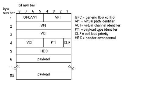
In this section we shall examine a hardware simulator for Asynchronous Transfer Mode ( ATM ). ATM is a signaling protocol for many different types of traffic including constant bit rates (voice signals) as well as variable bit rates (compressed video). The ATM Connection Simulator is a card that is connected to a computer. Under computer control the card monitors and corrupts the ATM signals to simulate the effects of real networks. An example would be to test different video compression algorithms. Compressed video is very bursty (brief periods of very high activity), has very strict delay constraints, and is susceptible to errors. ATM is based on ATM cells (packets). Each ATM cell has 53 bytes: a 5-byte header and a 48-byte payload; Figure 15.4 shows the format of the ATM packet. The ATM Connection Simulator looks at the entire header as an address.
FIGURE 15.4 The asynchronous transfer mode (ATM) cell format. The ATM protocol uses 53-byte cells or packets of information with a data payload and header information for routing and error control.
Figure 15.5 shows the system block diagram of the ATM simulator designed by Craig Fujikami at the University of Hawaii. Now produced by AdTech, the simulator emulates
the characteristics of a single connection in an ATM network and models ATM traffic policing, ATM cell delays, and ATM cell errors. The simulator is partitioned into the three major blocks, shown in Figure 15.5 , and connected to an IBM-compatible PC through an Intel 80186 controller board together with an interface board. These three blocks are
FIGURE 15.5 An asynchronous transfer mode (ATM) connection simulator.
●The traffic policer, which regulates the input to the simulator.
●The delay generator, which delays ATM cells, reorders ATM cells, and inserts ATM cells with valid ATM cell headers.
●The error generator, which produces bit errors and four random variables that are needed by the other two blocks.
The error generator performs the following operations on ATM cells:
1.Payload bit error ratio generation. The user specifies the Bernoulli probability, p BER , of the payload bit error ratio.
2.Random-variable generation for ATM cell loss, misinsertion, reordering, and

deletion.
The delay generator delays, misinserts, and reorders the target ATM cells. Finally, the traffic policer performs the following operations:
1.Performs header screening and remapping.
2.Checks ATM cell conformance.
3.Deletes selected ATM cells.
Table 15.7 shows the partitioning of the ATM board into 12 Lattice Logic FPGAs (ispLSI 1048) corresponding to the 12 blocks shown in Figure 15.5 . The Lattice Logic ispLSI 1048 has 48 GLBs (generic logic blocks) on each chip. This system was partitioned by hand with difficulty. Tools for automatic partitioning of systems like this will become increasingly important. In Section 15.6.2 we shall briefly look at some examples of such tools, before examining the partitioning methods that are used in Section 15.7 .
TABLE 15.7 Partitioning of the ATM board using Lattice Logic ispLSI 1048 FPGAs. Each FPGA contains 48 generic logic blocks (GLBs).
Chip # |
Size |
Chip # |
Size |
1 |
42 GLBs |
7 |
36 GLBs |
2 |
64 k-bit ¥ 8 SRAM |
8 |
22 GLBs |
3 |
38 GLBs |
9 |
256 k-bit ¥ 16 SRAM |
4 |
38 GLBs |
10 |
43 GLBs |
5 |
42 GLBs |
11 |
40 GLBs |
6 |
64 k-bit ¥ 16 SRAM |
12 |
30 GLBs |
15.6.2 Automatic Partitioning with FPGAs
Some vendors of programmable ASICs provide partitioning software. For example, Altera uses its own software system for design. You can perform design entry using an HDL, schematic entry, or using the Altera hardware design language (AHDL) similar to PALASM or ABEL. In AHDL you can direct the partitioner to automatically partition logic into chips within the same family, using the AUTO keyword:
DEVICE top_level IS AUTO; % the partitioner assign logic
You can use the CLIQUE keyword to keep logic together (this is not quite the same as a clique in a graph more on this in Section 15.7.3 ):
CLIQUE fast_logic
BEGIN
|shift_register: MACRO; % keep this in one device
END;
An additional option, to reserve space on a device, is very useful for making last minute additions or changes.
15.9 Problems
* = Difficult, ** = Very difficult, *** = Extremely difficult
15.1(Complexity, 10 min.) Suppose the workstations we use to design ASICs increase in power (measured in MIPS a million instructions per second) by a factor of 2 every year. If we want to keep the length of time to solve an ASIC design problem fixed, calculate how much larger chips can get each year if constrained by an algorithm with the following complexities:
●a. O (k).
●b. O (n).
●c. O(log n ).
●d. O( n log n ).
●e. O( n 2 ).
15.2(Complexity, 10 min.) In a film the main character looks 12 moves ahead to win a chess championship.
●a. Estimate (stating your assumptions) the number of possible chess moves looking 12 moves ahead.
●b. How long would it take to evaluate all these moves on a modern workstation?
15.3(Chips and towns, 20 min.) This problem is adapted from an analogy credited to Chuck Seitz. Complete the entries in Table 15.8 , which shows the
progression of integrated circuit complexity using the analogy of town and city planning. If l is half the minimum feature size, assume that a transistor is a square 2 l on a side and is equivalent to a city block (which we estimate at 200 m on a side).
TABLE 15.8 Complexity of ASICs (Problems 15.3 and 15.4 ).
|
Chip |
|
|
City size |
|
|
|
|
|
(km on a |
|
||
Year l / m m |
size |
Transistor size |
Transistors = city |
|
||
|
|
side, |
Example |
|||
(mm on |
( m m on a side) blocks |
|||||
|
1 block = |
|
||||
|
a side) |
|
|
|
||
|
|
|
|
200m) |
|
|
1970 50 |
5 |
200 |
25 ¥ 25 = 625 |
5 |
Palo Alto |
|
1980 5 |
10 |
20 |
500 ¥ 500 = 25 ¥ |
|
|
|
10 3 |
|
|
||||
|
|
|
|
|
||
1990 |
0.5 |
20 |
1,000 ¥ 1,000 = 1 ¥ |
||
1 |
6 |
|
|||
|
|
|
10 |
|
|
2000 |
0.05 |
40 |
20,000 ¥ 20,000 = |
||
0.2 |
|
6 |
|||
|
|
|
400 ¥ 10 |
||
15.4(Polygons, 10 min.) Estimate (stating and explaining all your assumptions) how many polygons there are on the layouts for each of the chips in Table 15.8 .
15.5(Algorithm complexity, 10 min.) I think of a number between 1 and 100. You guess the number and I shall tell you whether you are high or low. We then repeat the process. If you were to write a computer program to play this game, what would be the complexity of your algorithm?
15.6(Algorithms, 60 min.) For each of these problems write or find (stating your source) an algorithm to solve the problem:
●a. An algorithm to sort n numbers.
●b. An algorithm to discover whether a number n is prime.
●c. An algorithm to generate a random number between 1 and n .
List the algorithm using a sequence of steps, pseudocode, or a flow chart. What is the complexity of each algorithm?
15.7(Measurement, 30 min.) The traveling-salesman problem is a well-known example of an NP-complete problem (you have a list of cities and their locations and you have to find the shortest route between them, visiting each only once). Propose a simple measure to estimate the length of the solution. If I had to visit the 50 capitals of the United States, what is your estimate of my frequent-flyer mileage?
15.8(Construction, 30 min.) Try and make a quantitative comparison (stating and explaining all your assumptions) of the difficulty and complexity of construction (for example, how many components in each?) for each of the following: a Boeing 747 jumbo jet, the space shuttle, and an Intel Pentium microprocessor. Which, in your estimation, is the most complex and why? Smailagic [ 1995] proposes measures of design and construction complexity in a description of the wearable computer project at Carnegie-Mellon University.
15.9(Productivity, 20 min.). If I have six months to design an ASIC:
●a. What is the productivity (in transistors/day) required for each of the chips in Table 15.8 ?
●b. What does this translate to in terms of a productivity increase (measured in percent increase in productivity per month)?
●c. Moore s Law says that chip sizes double every 18 months. What does this correspond to in terms of a percentage increase per month?
●d. Comment on your answers.
15.10 (Graphs and edges, 30 min.) We know a net with two connections requires a single edge in the network graph, a net with three connections requires three edges, and a net with four connections requires six edges.
●a. Can you guess a formula for the number of edges in the network graph corresponding to a net with n connections?
●b. Can you prove the formula you guessed in part a? Hint: How many edges are there from one node to n 1 other nodes?
●c. Large nets cause problems for partitioning algorithms based on a connectivity matrix (edges rather than wires). Suppose we have a 50-net connection that is no more critical for timing than any other net. Suggest a way to fool the partitioning algorithm so this net does not drag all its logic cells into one partition.
Most CAD programs treat large nets (like the clock, reset, or power nets) separately, but the nets are required to have special names and you only can have a limited number of them. The average net in an ASIC has between two and four connections and as a rule of thumb 80 percent of nets have a fanout of 4 or less (a fanout of 4 means a gate drives four others, making a total of five connections on the net).
15.11 (PC partitioning, 60 min.) Open an IBM-compatible PC, Apple Macintosh, or PowerPC that has a motherboard that you can see easily. Make a list of the chips (manufacturer and type), their packages, and pin counts. Make intelligent guesses as to the function of most of the chips. Obviously manufacturer s logos and chip identification markings help perhaps they are in a data book. Identify the types of packages (pin-grid array, quad flat pack). Look for nearby components that may give a hint crystals for clock generators or the video subsystem. Where are the chips located on the board are they near the connectors for the floppy disk subsystem, the modem or serial port, or video output? To help you, Table 15.9 shows an example a list of the first row of chips on an old H-P Vectra ES/12 motherboard. Use the same format for your list.
TABLE 15.9 A list of the chips on the first row of an HP Vectra PC (Problem 15.11 ).
Manufacturer Chip |
Package |
Function |
Comment |
||
HP |
87411AAE |
24-pin DIP |
|
|
|
Intel |
L7220048 |
40-pin DIP |
EPROM (9/3/87) |
Boot commands |
|
Chips |
7014-0093 |
80-pin quad |
Custom ASIC |
|
|
|
|
flat pack |
|
|
|
Intel |
80286-12 |
68-pin |
Microprocessor |
CPU |
|
package |
|||||
|
|
|
|
||
TI |
AS00 |
14-pin DIP |
Quad 2-input NAND |
Addressing |
|
gate |
|||||
|
|
|
|
||
|
S74F08D |
14-pin DIP |
Quad 2-input AND gate |
Addressing |
|
|
F74F51 |
14-pin DIP |
AOI gate |
Addressing |
|
15.12 (Estimates, 60 min.) System partitioning is not exact science. Estimate:
●a. The power developed by a grasshopper, in watts (from a Cambridge University entrance exam).
●b. The number of doors in New York City.
●c. The number of grains of sand on Hawaii s beaches.
●d. The total length of the roads in the continental United States in kilometers.
In each case: (i) Provide an equation that depends on parameters and symbols that you define. (ii) List the parameters in your equation, and the values that you assume with their uncertainty. (iii) Give the answer as a number (with units where necessary). (iv) Include a numerical estimate of the uncertainty in your answer.
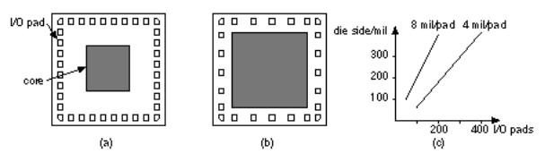
15.13 (Pad-limited and core-limited die, 10 min.) As the number of I/O pads increases, an ASIC can become pad-limited. The spacing between I/O pads is determined by mechanical limitations of the equipment used for bonding usually 2 5 mil (a mil is a thousandth of an inch). In a pad-limited design the number of pads around the outer edge of the die determines the die size, not the number of gates (see Figure 15.12 ). For the pad-limited design, shown in Figure 15.12 (a), the price per I/O pad is more important than the price per gate. When we have a lot of logic but few I/O pads, we have a core-limited design the opposite of a pad-limited ASIC as shown in Figure 15.12 (b). For a given number of I/O pads and a pad-limited design, all the different ASIC types will have the same die size, determined by a graph such as the one shown in Figure 15.12 (c). If I/O pad
spacing is 5 mil and gate density is 1.0 gate/mil 2 , when does an ASIC becomes pad-limited? Express your answer as a function of the number of gates, G , and the number of I/Os, I .
FIGURE 15.12 Die size. (a) A pad-limited die, the die size is determined by the number of I/O pads. (b) A core-limited die, the die size is limited by the amount of logic in the core. (c) For a given pad spacing we can determine the die size for a pad-limited die.
15.14 (Estimating ASIC size, 120 min.) Let us pretend we are going to build a laptop SPARCstation. We need to drastically reduce the number of chips used in the desktop system. Focus on the I/O subsystems in Figure 15.2 (chip labels are
shown in parentheses): LANCE Ethernet controller (14), 3C90 SCSI controller (15), 85C30 serial port controller (16, 17), 79C30 ISDN interface (18), and 82072 floppy-disk controller (19). Consider combining these functions into a single custom ASIC.
●a. Collect as much data as you can on the ASSP chips (14 19) that are currently used in the SPARCstation 1, similar to that presented in
Table 15.5 . National Semiconductor, Texas Instruments, AMD, Intel, and Motorola produce these or similar chips. You will need one or more of their ASSP data books. Try to find the pin count, power dissipation, and gate count for each chip. If you can t find one of these parameters, make an estimate and explain your assumptions.
●b. Using your data, make an estimate of the size, power dissipation, and pin count of the ASIC to replace chips 14 19 in Figure 15.2 .
●c. As a sanity check compare your results with the DMA2 Ethernet, SCSI, and parallel port chip in the SPARCstation 10 (see Table 15.2 ). This is a 30 k-gate array in a 160-pin quad flat pack.
15.15 (Power dissipation, 20 min.) If a Pentium microprocessor dissipates 5 W and, on average, 20 percent of the circuit nodes toggle every clock cycle
●a. Calculate the total capacitance of all the circuit nodes in picofarads if the clock frequency is 100 MHz and V DD = 5 V.
●b. If half of this is due to interconnect capacitance at 2 pFcm 1 , what is the total length of interconnect?
●c. If there are 100 I/Os driving an average of 20 pF load off-chip at an average frequency of 50 MHz, what is the power dissipation in the I/Os?
●d. A Pentium chip contains about 3 ¥ 10 6 transistors. How many gates is this?
●e. How many gates are switching on average every clock cycle?
15.16 (Parasitic power dissipation, 20 min.) Consider the following arguments: The energy stored in a capacitor is 1/2( CV 2 ) (measured in joules). Suppose we charge and discharge a capacitance C between zero and V volts at a frequency f . We have to replace this energy f times per second and we shall dissipate a power (measured in watts) equal to
P = 0.5 f CV DD 2 (15.23)
When the p -channel transistor in an inverter is charging a capacitance, C , at a frequency, f , the current through the transistor is C (d V /d t ), the power dissipation is CV (d V /d t ) for one-half the period of the input, t = 1/(2 f ). The power dissipated in the p -channel transistor is thus
1/(2f) |
d V |
P = f Ú |
CV d t = 0.5 fCV DD 2 (15.24) |
0 |
d t |
During the second half-period of the input signal the p -channel transistor is off, so that there can be no power dissipation in the power supply. The power dissipation that occurs in the n -channel transistor must come from the stored energy in the capacitor which is accounted for in the equation. In both cases the total power dissipation should be 1/2( fCV 2 ), not ( fCV 2 ) as we have stated in Eq. 15.4 . Point out the errors in both of these arguments. (If you are interested in situations in which these equations do hold, you can search for the term adiabatic logic.)
15.17 (Short-circuit power dissipation, 30 min.) Prove Eq. 15.5 as follows: The input to a CMOS inverter is a linear ramp with rise time t rf . Calculate the n -channel transistor current as a function of the input voltage, V in , assuming the n -channel transistor turns on when V in = V t n and the current reaches a maximum when V in = V DD / 2 at t = t rf / 2.
The transistor current is given by Eq. 2.9. Assume b = ( W/L ) m Cox is the same for both p - and n -channel transistors, the magnitude of the threshold voltages | V t n | are assumed equal for both transistor types, and t is the rise time and fall time (assumed equal) of the input signal.
Show that for a CMOS inverter (Eq. 15.5 ):
P 2 = (1/12) b f t rf (V DD 2 Vt n ) 3 (15.25)
where b = ( W/L ) m Cox is the same for both p - and n -channel transistors, the magnitude of the threshold voltages | V t n | are assumed equal for both transistors, and t is the rise time and fall time (assumed equal) of the input signal [ Veendrick, 1984].
15.18 (Connectivity matrix, 10 min.) Find the connectivity matrix for the ATM Connection Simulator shown in Figure 15.5 . Use the following scheme to number the blocks and ordering of the matrix rows and columns: 1 = Personal Computer, 2 = Intel 80186, 3 = UTOPIA receiver, 4 = UTOPIA transmitter, 5 = Header remapper and screener, 6 = Remapper SRAM, . . . 15 = Random-number and bit error rate generator, 16 = Random-variable generator. All buses are labeled with their width except for two single connections (the arrows).
15.19 (K L algorithm, 15 min.)
● a. Draw the network graph for the following connectivity matrix: 0 0 0 0 0 0 1 0 0 0 0 0 0 0 0 1 0 1 0 0 0 0 0 1 0 0 0 1 0 0 0 0 1 0 1 0 0 0 1 0
C = 0 0 0 1 0 0 0 0 0 0 (15.26)
0 1 0 0 0 0 0 0 1 0
1 0 0 0 0 0 0 0 1 0
0 1 1 0 0 0 0 0 1 0
0 0 0 1 0 0 1 1 0 1
0 0 0 0 0 0 0 0 1 0
●b. Draw the partitioned network graph for C with nodes 1 5 in partition A and nodes 6 10 in partition B. What is the cut weight?
●c. Improve the initial partitioning using the K L algorithm. Show the gains at each stage. What problems did you find in following the algorithm and how do you resolve them?
15.20 (The gain graph in the K L algorithm, 20 min.). Continue with the K L algorithm for the network that we started to partition in Figure 15.9 (a).
● a. Show that choices of logic cells to swap and the gains correspond to the graph of Figure 15.9 (b).
● b. Notice that G 5 = 0. In fact G m (where there are 2 m nodes to be partitioned) will always be zero. Can you explain why?
15.21 (Look-ahead gain in the K L algorithm, 20 min.) In the K L algorithm we have to compute the gain each time we consider swapping one pair of nodes:
g 1 = D a + D b 2 c ab . (15.27)
If we swap two pairs of nodes ( a 1 and b 1 followed by a 2 and b 2 ), show that the gain is
D a 2 |
+ D b 2 2 c a 2 b 2 |
2 c a 2 a 1 |
2 c a 2 b 1 |
2 c b 2 a 1 |
+ 2 c b 2 b |
(15.28) |
g 1 = |
|
|
|
|
|
|
1 . |
|
|
|
|
|
|
15.22 (FPGA partitioning, 30 min.) Table 15.10 shows some data on FPGAs from company Z.
TABLE 15.10 FPGAs from company Z (Problem 15.22 ).
FPGA size Die area / cm 2 Average gate count Package pins Cost
S |
0.26 |
1500 |
68 |
$26 |
M |
0.36 |
2300 |
44 |
$35 |
L |
0.46 |
2800 |
84 |
$50 |
XL |
0.64 |
4700 |
84 |
$90 |
XXL |
0.84 |
6200 |
84 |
$130 |
●a. Notice that the FPGAs come in different package sizes. To eliminate the effect of package price, multiply the price for the S chip by 106 percent, and the M chip by 113 percent. Now all prices are normalized for an 84-pin plastic package. All the chips are the same speed grade; if they were not, we could normalize for this too (a little harder to justify though).
●b. Plot the normalized chip prices vs. gate count. What is the cost per gate?
●c. The part cost ought to be related to the yield, which is directly related to die area. If the cost of a 6-inch-diameter wafer is fixed (approximately $1000), calculate the cost per die, assuming a yield Y (in percent), as a function of the die area, A (in cm 2 ). Assume you completely fill the wafer and you can have fractional die (i.e., do not worry about packing square die into a circular wafer).
●d. There are many models for the yield of a process, Y . Two common models are
Y = exp [ ÷ (AD) ] . (15.29)
and |
|
|
Ê |
1 exp ( AD )Æ 2 |
|
Y = Á |
|
Ü (15.30) |
Ë |
AD |
¯ |
Parameter A is the die area in cm 2 and D is the spot defect density in defects/cm 2 and is usually around 1.0 defects/cm 2 for a good submicron CMOS process (above 5.0 defects/cm 2 is unusual). The most important thing is the yield; anything below about 50 percent good die per wafer is usually bad news for an ASIC foundry. Does the FPGA cost data fit either model?
●e. Now disregard the current pricing strategy of company Z. If you had to bet that physics would determine the true price of the chip, how much worse or better off are you using two small FPGAs rather than one larger FPGA (assume the larger die is exactly twice the area of the smaller one) under these two yield models?
●f. What assumptions are inherent in the calculation you made in part
e? How much do you think they might affect your answer, and what else would affect your judgment?
●g. Give some reasons why you might select two smaller FPGAs rather than a larger FPGA, even if the larger FPGA is a cheaper solution.
●h. Give some reasons why you would select a larger FPGA rather than two smaller FPGAs, even if the smaller FPGAs were a cheaper solution.
15.23 (Constructive partitioning, 30 min.) We shall use the simple network with 12 blocks shown in Figure 15.7 to experiment with constructive partitioning. This example is topologically equivalent to that used in [Goto and Matsud, 1986].
●a. We shall use a gain function, g(m) , calculated as follows: Sum the number of the nets (not connections ) from the selected logic cell, m , that connect to the current partition call this P(m). Now calculate the number of nets that connect logic cell m to logic cells which are not yet in partitionscall this N(m). Then g(m) = P(m) N(m) is the gain of adding the logic cell m to the partition currently being filled.
●b. Partition the network using the seed growth algorithm with logic cell C as the seed. Show how this choice of seed can lead to the partitioning shown in Figure 15.7 (c). Use a table like Table 15.11 as a bookkeeping aid (a spreadsheet will help too). Each row corresponds to a pass through the algorithm. Fill in the measures, P(m) N(m), equal to the gain, g(m). Once a logic cell is assigned to a partition, fill in the name of the partition (X, Y, or Z) in that column. The first row shows you how logic cell L is selected; proceed from there. What problems do you encounter while completing the algorithm, and how do you resolve them?
●c. Now partition using logic cell F as the seed instead the logic cell with the highest number of nets. When you have a tie between logic cells with the same gain, or you are starting a new partition, pick the logic cell with the largest P(m) . Use a copy of Table 15.12 as a bookkeeping aid. How does your partition compare with those we have already made (summarized in Table 15.13 )?
●d. Comment on your results.
Table 15.14 will help in constructing the gain function at each step of the algorithm.
TABLE 15.11 Bookkeeping table for Problem 15.23 ( b ).
Pass Gain A B |
C D E F G H I J |
K L |
||
1 |
P N0 21 2X |
0 21 40 50 20 20 30 30 20 1 |
||
|
= g = 2 = 1 |
|
= 2 = 3 = 5 = 2 = 2 = 3 = 3 = 2 = 1 |
|
2 |
|
X |
X |
X |
TABLE 15.12 Bookkeeping table for Problem 15.23 ( c ).
Pass Gain |
A B C D E |
F |
G H I J K L |
1 P N = g |
1 20 21 11 11 3X |
0 21 22 20 30 20 1 |
|
|
= 1 = 2 = 0 = 0 = 2 |
|
= 2 = 1 = 0 = 3 = 2 = 1 |
2 |
|
X |
X |
|
TABLE 15.13 Different partitions for the network shown in Figure 15.7 |
||||
(Problem 15.23 c ). |
|
|
|
|
|
Total external |
|
Partition |
Connections to each |
Partitioning |
|
contents |
||
|
|
|||
connections |
|
|
partition |
|
|
|
X, Y, Z |
||
|
|
|
||
|
|
|
|
|
|
|
|
X = (A, B, C, |
|
|
|
|
L) |
3 |
|
5 |
|
|
|
Figure 15.7 (b) |
|
Y = (D, F, H, |
3 |
|
|
|
|||
(2, 4, 5, 6, 8) |
|
I) |
||
|
|
|
||
|
|
|
|
|
4
Z = (E, G, J, K)
|
X = (A, B, F, |
|
|
D) |
5 |
Figure 15.7 (c) |
7 |
|
Y = (H, I, J, K) 5 |
||
|
(2, 3, 5, 7, 9, 11, 12) |
|
|
Z = (C, E, G, |
4 |
L)
TABLE 15.14 An aid to calculating the gains for Problem 15.23 .
Logic cell |
Connects to: |
Number of nets |
Number of |
|
connections |
||||
|
|
|
||
A |
B, F |
2 |
2 |
|
B |
A, (C, E) |
2 |
3 |
|
C |
(B, E) |
1 |
2 |
|
D |
F, H |
2 |
2 |
|
E |
(B, C), F, (G, L), J |
4 |
6 |
|
F |
A, D, E, (H, I1), I2 |
5 |
6 |
|
G |
(E, L), (J, K) |
2 |
4 |
|
H |
D, (F, I) |
2 |
3 |
|
I |
F1, (F2, H), (J, K) |
3 |
5 |
|
J |
E, (G, K1), (I, K2) |
3 |
5 |
|
K |
(G, J1), (I, J2) |
2 |
4 |
|
L |
(E, G) |
1 |
2 |
15.24 (Simulated annealing, 15 min.) If you have a fixed amount of time to solve a partitioning problem, comment on the following alternatives and choose one:
i.Run a single simulated annealing cycle using a slow cooling schedule.
ii.Run several (faster) min-cut based partitionings, using different seeds, and pick the best one.
iii.Run several simulated annealing cycles using a faster cooling schedule, and pick the best result.
15.25 (Net weights, 15 min.) Figure 15.13 shows a small part of a system and will help illustrate some potential problems when you weight nets for partitioning. Nets s1 s3 are critical, nets c1 c4 are not. Assume that all nets are weighted by a cost of one unless the special net weight symbol is attached.
●a. Explain the problem with the net weights as shown in Figure 15.13 (a).
●b. Figure 15.13 (b) shows a different way to assign weights. What problems might this cause in the rest of the system?
●c. Figure 15.13 (c) shows another possible solution. Discuss the advantages of this approach.
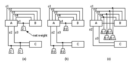
● d. Can you think of another way to solve the problem?
This situation represents a very real problem with using net weights and tools that use min-cut algorithms. As soon as you get one critical net right, the tool makes several other nets too long and they become critical. The problem is worse during system partitioning when the blocks are big and there are many different nets with differing importance attached to each block but it can happen during floorplanning and placement also.
FIGURE 15.13 (For Problem 15.25 .) An example of a problem in weighting nets. The symbols attached to the nets apply a weight or cost to that net during partitioning. Nets c1 c4 are control lines they are not critical for timing purposes. Nets s1 s3 are signal lines that are critical they must be kept short. The figure shows three different ways to handle this using net weights.
15.26 (Cost, 60 min.) You have three chip sizes available for your part of projectDreamOn (a new video game): S, M, and L. The L chip has twice the logic of the M chip. The M chip has twice the logic of the S chip. The L chip costs $16, which is 4 times as much as the M chip and 16 times as much as the S chip. There are two speed grades available: fast (F) and turbocharged (T). The T chip costs twice as much as the F version. Using a partitioning program, you find you need the equivalent of 1.8 of the L chips, but only a third of your logic needs a T chip.
●a. What is the cheapest way to build DreamOn ?
●b. During prototyping you find you can use 90 percent of the S and M type chips, but for reliable routing you can only count on a maximum utilization of 85 percent for the L chip. You also find that, to maximize performance, you need to keep all of the logic that requires the turbo speed on one chip. Our ASIC vendor, Xactera, promises us that the chip prices will fall by the time we go into production in one year. The estimates are that the prices will be almost proportional to chip size: The L chip will cost 2.2 times the M chip and 4.4 times whatever is the cost of the S chip by then (but Xactera will not commit to a future price for the S chip, only the present price). You predict the price of the S chip will fall 20 percent in one year

(this is about average for the annual rate of price decrease for semiconductors). Xactera says the turbocharged speed grade will stay about twice the cost of the fast grade. How does this information affect your decision?
●c. Some time later, as you are ready to go on vacation, the production department tells you that the board cost is about the same as the chip cost! The board area does not make much difference to the price, but there is an extra charge per package pin to reflow solder the surface-mount chips. We only need each chip to have the minimum size package a 44-pin quad plastic package. Production has two price quotes: Boards-R-Us charges $5 per board plus $0.01 per pin, and PCB Inc. quotes at $0.05 per pin. What should we do? The CEO needs a recommendation today.
●d. You come back from holiday and find out from your e-mail that we went with your recommendation on the board vendor but now we have other problems. The test company is charging per chip pin on the board since we are using an old style bed-of-nails tester. The cost is about $0.01 per chip pin. You can go back and add a test interface to all the chips, which is the equivalent of adding 10 percent of a small chip (type S) on each chip (S, M, or L). This would eliminate the bed-of-nails test, and reduce board test cost to $1 per board. Xactera also just lowered their prices: L chips are now $4, M chips are $2, and S chips are $0.95. There is also a new Xactera XL chip that has twice the capacity of the L chips and costs $8 (but you do not know what utilization to expect). These prices are for the fast speed grades, the turbo versions are now 2.5 times more expensive.
●e. There are some serious consequences to making any design changes now (including schedule slips). We have an emergency meeting with production, finance, marketing, and the CEO this afternoon in the boardroom. I have to prepare a presentation outlining our past decisions and the advantages and disadvantages of each of our options (with quantitative estimates of their effect). Can you prepare four foils for me, and a one-page spreadsheet that will allow us to make some rapid what-if decisions in the meeting? Print the foils and the one-page spreadsheet.
●f. A year later we are in full production and all is well. We are reviewing your performance on project DreamOn. What did you learn from this project and how would you do things differently next time? (You only have room for 100 words on your review form.)