

16.2 Placement
After completing a floorplan we can begin placement of the logic cells within the flexible blocks. Placement is much more suited to automation than floorplanning. Thus we shall need measurement techniques and algorithms. After we complete floorplanning and placement, we can predict both intrablock and interblock capacitances. This allows us to return to logic synthesis with more accurate estimates of the capacitive loads that each logic cell must drive.
16.2.1 Placement Terms and Definitions
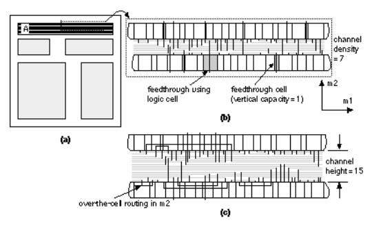
CBIC, MGA, and FPGA architectures all have rows of logic cells separated by the interconnect these are row-based ASICs . Figure 16.18 shows an example of the interconnect structure for a CBIC. Interconnect runs in horizontal and vertical directions in the channels and in the vertical direction by crossing through the logic cells. Figure 16.18 (c) illustrates the fact that it is possible to use over-the-cell routing ( OTC routing) in areas that are not blocked. However, OTC routing is complicated by the fact that the logic cells themselves may contain metal on the routing layers. We shall return to this topic in Section 17.2.7, Multilevel Routing. Figure 16.19 shows the interconnect structure of a two-level metal MGA.
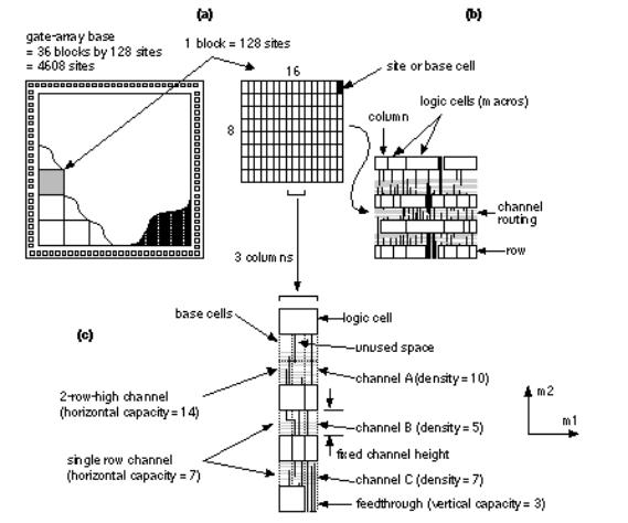
FIGURE 16.18 Interconnect structure. (a) The two-level metal CBIC floorplan shown in Figure 16.11 b. (b) A channel from the flexible block A. This channel has a channel height equal to the maximum channel density of 7 (there is room for seven interconnects to run horizontally in m1). (c) A channel that uses OTC (over-the-cell) routing in m2.
Most ASICs currently use two or three levels of metal for signal routing. With two layers of metal, we route within the rectangular channels using the first metal layer for horizontal routing, parallel to the channel spine, and the second metal layer for the vertical direction (if there is a third metal layer it will normally run in the horizontal direction again). The maximum number of horizontal interconnects that can be placed side by side, parallel to the channel spine, is the channel capacity .
FIGURE 16.19 Gate-array interconnect. (a) A small two-level metal gate array (about 4.6 k-gate). (b) Routing in a block. (c) Channel routing showing channel density and channel capacity. The channel height on a gate array may only be increased in increments of a row. If the interconnect does not use up all of the channel, the rest of the space is wasted. The interconnect in the channel runs in m1 in the horizontal direction with m2 in the vertical direction.
Vertical interconnect uses feedthroughs (or feedthrus in the United States) to cross the logic cells. Here are some commonly used terms with explanations (there are no generally accepted definitions):
●An unused vertical track (or just track ) in a logic cell is called an uncommitted feedthrough (also built-in feedthrough , implicit feedthrough , or jumper ).
●A vertical strip of metal that runs from the top to bottom of a cell (for double-entry cells ), but has no connections inside the cell, is also called a feedthrough or jumper.
●Two connectors for the same physical net are electrically equivalent connectors (or equipotential connectors ). For double-entry cells these are usually at the top and bottom of the logic cell.
●A dedicated feedthrough cell (or crosser cell ) is an empty cell (with no logic) that can hold one or more vertical interconnects. These are used if there are no other feedthroughs available.
●A feedthrough pin or feedthrough terminal is an input or output that has connections at both the top and bottom of the standard cell.
●A spacer cell (usually the same as a feedthrough cell) is used to fill space in rows so that the ends of all rows in a flexible block may be aligned to connect to power buses, for example.
There is no standard terminology for connectors and the terms can be very confusing. There is a difference between connectors that are joined inside the logic cell using a high-resistance material such as polysilicon and connectors that are joined by low-resistance metal. The high-resistance kind are really two separate alternative connectors (that cannot be used as a feedthrough), whereas the low-resistance kind are electrically equivalent connectors. There may be two or more connectors to a logic cell, which are not joined inside the cell, and which must be joined by the router ( must-join connectors ).
There are also logically equivalent connectors (or functionally equivalent connectors, sometimes also called just equivalent connectors which is very confusing). The two inputs of a two-input NAND gate may be logically equivalent connectors. The placement tool can swap these without altering the logic (but the two inputs may have different delay properties, so it is not always a good idea to swap them). There can also be logically equivalent connector groups . For example, in an OAI22 (OR-AND-INVERT) gate there are four inputs: A1, A2 are inputs to one OR gate (gate A), and B1, B2 are inputs to the second OR gate (gate B). Then group A = (A1, A2) is logically equivalent to group B = (B1, B2) if we swap one input (A1 or A2) from gate A to gate B, we must swap the other input in the group (A2 or A1).
In the case of channeled gate arrays and FPGAs, the horizontal interconnect areas the channels, usually on m1 have a fixed capacity (sometimes they are called fixed-resource ASICs for this reason). The channel capacity of CBICs and channelless MGAs can be expanded to hold as many interconnects as are needed. Normally we choose, as an objective, to minimize the number of interconnects that use each channel. In the vertical interconnect direction, usually m2, FPGAs still have fixed resources. In contrast the placement tool can always add vertical feedthroughs to a channeled MGA, channelless MGA, or CBIC. These problems become less important as we move to three and more levels of interconnect.
16.2.2 Placement Goals and Objectives
The goal of a placement tool is to arrange all the logic cells within the flexible blocks on a chip. Ideally, the objectives of the placement step are to
●Guarantee the router can complete the routing step
●Minimize all the critical net delays
●Make the chip as dense as possible
We may also have the following additional objectives:
●Minimize power dissipation
●Minimize cross talk between signals
Objectives such as these are difficult to define in a way that can be solved with an algorithm and even harder to actually meet. Current placement tools use more specific and achievable criteria. The most commonly used placement objectives are one or more of the following:
●Minimize the total estimated interconnect length
●Meet the timing requirements for critical nets
●Minimize the interconnect congestion
Each of these objectives in some way represents a compromise.
16.2.3 Measurement of Placement Goals
and Objectives
In order to determine the quality of a placement, we need to be able to measure it. We need an approximate measure of interconnect length, closely correlated with the final interconnect length, that is easy to calculate.
The graph structures that correspond to making all the connections for a net are known as trees on graphs (or just trees ). Special classes of trees Steiner treesminimize the total length of interconnect and they are central to ASIC routing algorithms. Figure 16.20 shows a minimum Steiner tree. This type of tree uses diagonal connections we want to solve a restricted version of this problem, using interconnects on a rectangular grid. This is called rectilinear routing or Manhattan routing (because of the east west and north south grid of streets in Manhattan). We say that the Euclidean distance between two points is the straight-line distance ( as the crow flies ). The Manhattan distance (or rectangular distance) between two points is the distance we would have to walk in New York.
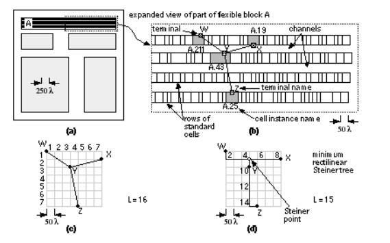
FIGURE 16.20 Placement using trees on graphs. (a) The floorplan from Figure 16.11 b. (b) An expanded view of the flexible block A showing four rows of standard cells for placement (typical blocks may contain thousands or tens of thousands of logic cells). We want to find the length of the net shown with four terminals, W through Z, given the placement of four logic cells (labeled: A.211, A.19, A.43, A.25). (c) The problem for net (W, X, Y, Z) drawn as a graph. The shortest connection is the minimum Steiner tree. (d) The minimum rectilinear Steiner tree using Manhattan routing. The rectangular (Manhattan) interconnect-length measures are shown for each tree.
The minimum rectilinear Steiner tree ( MRST ) is the shortest interconnect using a rectangular grid. The determination of the MRST is in general an NP-complete problem which means it is hard to solve. For small numbers of terminals heuristic algorithms do exist, but they are expensive to compute. Fortunately we only need to estimate the length of the interconnect. Two approximations to the MRST are shown in Figure 16.21 .
The complete graph has connections from each terminal to every other terminal [ Hanan, Wolff, and Agule, 1973]. The complete-graph measure adds all the interconnect lengths of the complete-graph connection together and then divides by n /2, where n is the number of terminals. We can justify this since, in a graph with n terminals, ( n 1) interconnects will emanate from each terminal to join the other ( n 1) terminals in a complete graph connection. That makes n ( n 1) interconnects in total. However, we have then made each connection twice. So there are one-half this many, or n ( n 1)/2, interconnects needed for a complete graph connection. Now we actually only need ( n 1) interconnects to join n terminals, so we have n /2 times as many interconnects as we really need. Hence we divide the total net length of the complete graph connection by n /2 to obtain a more reasonable estimate of minimum interconnect length. Figure 16.21 (a) shows an example of the complete-graph measure.
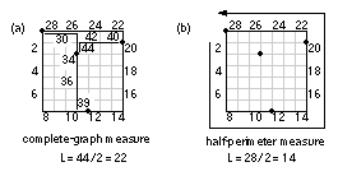
FIGURE 16.21 Interconnect-length measures. (a) Complete-graph measure. (b) Half-perimeter measure.
The bounding box is the smallest rectangle that encloses all the terminals (not to be confused with a logic cell bounding box, which encloses all the layout in a logic cell). The half-perimeter measure (or bounding-box measure) is one-half the perimeter of the bounding box ( Figure 16.21 b) [ Schweikert, 1976]. For nets with two or three terminals (corresponding to a fanout of one or two, which usually includes over 50 percent of all nets on a chip), the half-perimeter measure is the same as the minimum Steiner tree. For nets with four or five terminals, the minimum Steiner tree is between one and two times the half-perimeter measure [ Hanan, 1966]. For a circuit with m nets, using the half-perimeter measure corresponds to minimizing the cost function,
1 m
f = S h i , (16.5) 2 i = 1
where h i is the half-perimeter measure for net i .
It does not really matter if our approximations are inaccurate if there is a good correlation between actual interconnect lengths (after routing) and our approximations. Figure 16.22 shows that we can adjust the complete-graph and half-perimeter measures using correction factors [ Goto and Matsuda, 1986]. Now our wiring length approximations are functions, not just of the terminal positions, but also of the number of terminals, and the size of the bounding box. One practical example adjusts a Steiner-tree approximation using the number of terminals [ Chao, Nequist, and Vuong, 1990]. This technique is used in the Cadence Gate Ensemble placement tool, for example.
FIGURE 16.22 Correlation between total length of chip interconnect and the half-perimeter and complete-graph measures.
One problem with the measurements we have described is that the MRST may only approximate the interconnect that will be completed by the detailed router. Some programs have a meander factor that specifies, on average, the ratio of the interconnect created by the routing tool to the interconnect-length estimate used by the placement tool. Another problem is that we have concentrated on finding estimates to the MRST, but the MRST that minimizes total net length may not minimize net delay (see Section 16.2.8 ).
There is no point in minimizing the interconnect length if we create a placement that is too congested to route. If we use minimum interconnect congestion as an additional placement objective, we need some way of measuring it. What we are trying to measure is interconnect density. Unfortunately we always use the term density to mean channel density (which we shall discuss in Section 17.2.2, Measurement of Channel Density ). In this chapter, while we are discussing placement, we shall try to use the term congestion , instead of density, to avoid any confusion.
One measure of interconnect congestion uses the maximum cut line . Imagine a horizontal or vertical line drawn anywhere across a chip or block, as shown in
Figure 16.23 . The number of interconnects that must cross this line is the cut size (the number of interconnects we cut). The maximum cut line has the highest cut size.
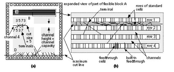
FIGURE 16.23 Interconnect congestion for the cell-based ASIC from Figure 16.11
(b). (a) Measurement of congestion. (b) An expanded view of flexible block A shows a maximum cut line.
Many placement tools minimize estimated interconnect length or interconnect congestion as objectives. The problem with this approach is that a logic cell may be placed a long way from another logic cell to which it has just one connection. This logic cell with one connection is less important as far as the total wire length is concerned than other logic cells, to which there are many connections. However, the one long connection may be critical as far as timing delay is concerned. As technology is scaled, interconnection delays become larger relative to circuit delays and this problem gets worse.
In timing-driven placement we must estimate delay for every net for every trial placement, possibly for hundreds of thousands of gates. We cannot afford to use anything other than the very simplest estimates of net delay. Unfortunately, the minimum-length Steiner tree does not necessarily correspond to the interconnect path that minimizes delay. To construct a minimum-delay path we may have to route with non-Steiner trees. In the placement phase typically we take a simple interconnect-length approximation to this minimum-delay path (typically the half-perimeter measure). Even when we can estimate the length of the interconnect, we do not yet have information on which layers and how many vias the interconnect will use or how wide it will be. Some tools allow us to include estimates for these parameters. Often we can specify metal usage , the percentage of routing on the different layers to expect from the router. This allows the placement tool to estimate RC values and delays and thus minimize delay.
16.2.4 Placement Algorithms
There are two classes of placement algorithms commonly used in commercial CAD tools: constructive placement and iterative placement improvement. A constructive placement method uses a set of rules to arrive at a constructed placement. The most commonly used methods are variations on the min-cut algorithm . The other commonly used constructive placement algorithm is the eigenvalue method. As in system partitioning, placement usually starts with a constructed solution and then improves it using an iterative algorithm. In most tools we can specify the locations
and relative placements of certain critical logic cells as seed placements .
The min-cut placement method uses successive application of partitioning [ Breuer, 1977]. The following steps are shown in Figure 16.24 :
1.Cut the placement area into two pieces.
2.Swap the logic cells to minimize the cut cost.
3.Repeat the process from step 1, cutting smaller pieces until all the logic cells are placed.
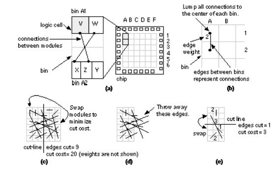
FIGURE 16.24 Min-cut placement. (a) Divide the chip into bins using a grid.
(b) Merge all connections to the center of each bin. (c) Make a cut and swap logic cells between bins to minimize the cost of the cut. (d) Take the cut pieces and throw out all the edges that are not inside the piece. (e) Repeat the process with a new cut and continue until we reach the individual bins.
Usually we divide the placement area into bins . The size of a bin can vary, from a bin size equal to the base cell (for a gate array) to a bin size that would hold several logic cells. We can start with a large bin size, to get a rough placement, and then reduce the bin size to get a final placement.
The eigenvalue placement algorithm uses the cost matrix or weighted connectivity matrix ( eigenvalue methods are also known as spectral methods ) [Hall, 1970]. The measure we use is a cost function f that we shall minimize, given by
1 n
f = S c ij d ij 2 , (16.6) 2 i = 1
where C = [ c ij ] is the (possibly weighted) connectivity matrix, and d ij is the Euclidean distance between the centers of logic cell i and logic cell j . Since we are going to minimize a cost function that is the square of the distance between logic

cells, these methods are also known as quadratic placement methods. This type of cost function leads to a simple mathematical solution. We can rewrite the cost function f in matrix form:
1 n
f = S c ij ( x i x j ) 2 + (y i y j ) 2 2 i = 1
= x T Bx + y T By . |
(16.7) |
In Eq. 16.7 , B is a symmetric matrix, the disconnection matrix (also called the
Laplacian).
We may express the Laplacian B in terms of the connectivity matrix C ; and D , a diagonal matrix (known as the degree matrix), defined as follows:
B = D C ; |
(16.8) |
n
d ii = S c ij , i = 1, ... , ni ; d ij = 0, i À j i = 1
We can simplify the problem by noticing that it is symmetric in the x - and y -coordinates. Let us solve the simpler problem of minimizing the cost function for the placement of logic cells along just the x -axis first. We can then apply this solution to the more general two-dimensional placement problem. Before we solve this simpler problem, we introduce a constraint that the coordinates of the logic cells must correspond to valid positions (the cells do not overlap and they are placed on-grid). We make another simplifying assumption that all logic cells are the same size and we must place them in fixed positions. We can define a vector p consisting of the valid positions:
p = [ p 1 , ..., p n ] . (16.9)
For a valid placement the x -coordinates of the logic cells,
x = [ x 1 , ..., x n ] . (16.10)
must be a permutation of the fixed positions, p . We can show that requiring the logic cells to be in fixed positions in this way leads to a series of n equations restricting the values of the logic cell coordinates [ Cheng and Kuh, 1984]. If we impose all of these constraint equations the problem becomes very complex. Instead we choose just one of the equations:
n |
n |
S |
x i 2 = S p i 2 . (16.11) |
i = 1 |
i = 1 |
Simplifying the problem in this way will lead to an approximate solution to the
placement problem. We can write this single constraint on the x -coordinates in matrix form:
n
x T x = P ; P = S p i 2 . (16.12) i = 1
where P is a constant. We can now summarize the formulation of the problem, with the simplifications that we have made, for a one-dimensional solution. We must minimize a cost function, g (analogous to the cost function f that we defined for the two-dimensional problem in Eq. 16.7 ), where
g = x T Bx . (16.13)
subject to the constraint:
x T x = P . (16.14)
This is a standard problem that we can solve using a Lagrangian multiplier:
L = x T Bx l [ x T x P] . (16.15)
To find the value of x that minimizes g we differentiate L partially with respect to x and set the result equal to zero. We get the following equation:
[ B l I ] x= 0 . (16.16)
This last equation is called the characteristic equation for the disconnection matrix B and occurs frequently in matrix algebra (this l has nothing to do with scaling). The solutions to this equation are the eigenvectors and eigenvalues of B . Multiplying Eq. 16.16 by x T we get:
l x T x = x T Bx . (16.17)
However, since we imposed the constraint x T x = P and x T Bx = g , then
l = g /P . (16.18)
The eigenvectors of the disconnection matrix B are the solutions to our placement problem. It turns out that (because something called the rank of matrix B is n 1) there is a degenerate solution with all x -coordinates equal ( l = 0) this makes some sense because putting all the logic cells on top of one another certainly minimizes the interconnect. The smallest, nonzero, eigenvalue and the corresponding eigenvector provides the solution that we want. In the two-dimensional placement problem, the x - and y -coordinates are given by the eigenvectors corresponding to the two smallest, nonzero, eigenvalues. (In the next section a simple example illustrates this mathematical derivation.)
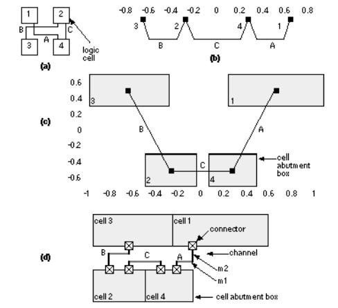

C=[0 0 0 1; 0 0 1 1; 0 1 0 0; 1 1 0 0]
D=[1 0 0 0; 0 2 0 0; 0 0 1 0; 0 0 0 2]
B=D-C
[X,D] = eig(B)
Running this script, we find the eigenvalues of B are 0.5858, 0.0, 2.0, and 3.4142. The corresponding eigenvectors of B are
0.6533 0.5000 0.5000 0.27060.27060.5000 0.5000 0.65330.65330.5000 0.5000 0.2706 0.2706 0.5000 0.50000.6533
(16.20)
For a one-dimensional placement ( Figure 16.25 b), we use the eigenvector (0.6533,0.2706, 0.6533, 0.2706) corresponding to the smallest nonzero eigenvalue (which is 0.5858) to place the logic cells along the x -axis. The two-dimensional placement ( Figure 16.25 c) uses these same values for the x -coordinates and the eigenvector (0.5,0.5, 0.5, 0.5) that corresponds to the next largest eigenvalue (which is 2.0) for the y -coordinates. Notice that the placement shown in Figure 16.25 (c), which shows logic-cell outlines (the logic-cell abutment boxes), takes no account of the cell sizes, and cells may even overlap at this stage. This is because, in Eq. 16.11 , we discarded
all but one of the constraints necessary to ensure valid solutions. Often we use the approximate eigenvalue solution as an initial placement for one of the iterative improvement algorithms that we shall discuss in Section 16.2.6 .
16.2.6 Iterative Placement Improvement
An iterative placement improvement algorithm takes an existing placement and tries to improve it by moving the logic cells. There are two parts to the algorithm:
●The selection criteria that decides which logic cells to try moving.
●The measurement criteria that decides whether to move the selected cells.
There are several interchange or iterative exchange methods that differ in their selection and measurement criteria:
●pairwise interchange,
●force-directed interchange,
●force-directed relaxation, and
●force-directed pairwise relaxation.
All of these methods usually consider only pairs of logic cells to be exchanged. A source logic cell is picked for trial exchange with a destination logic cell. We have already discussed the use of interchange methods applied to the system partitioning step. The most widely used methods use group migration, especially the Kernighan
Lin algorithm. The pairwise-interchange algorithm is similar to the interchange algorithm used for iterative improvement in the system partitioning step:
1.Select the source logic cell at random.
2.Try all the other logic cells in turn as the destination logic cell.
3.Use any of the measurement methods we have discussed to decide on whether to accept the interchange.
4.The process repeats from step 1, selecting each logic cell in turn as a source logic cell.
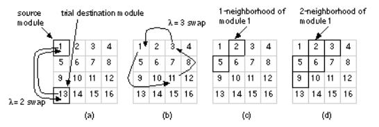
Figure 16.26 (a) and (b) show how we can extend pairwise interchange to swap more than two logic cells at a time. If we swap l logic cells at a time and find a locally optimum solution, we say that solution is l -optimum . The neighborhood exchange algorithm is a modification to pairwise interchange that considers only destination logic cells in a neighborhood cells within a certain distance, e, of the source logic cell. Limiting the search area for the destination logic cell to the e -neighborhood reduces the search time. Figure 16.26 (c) and (d) show the oneand two-neighborhoods (based on Manhattan distance) for a logic cell.
FIGURE 16.26 Interchange. (a) Swapping the source logic cell with a destination logic cell in pairwise interchange. (b) Sometimes we have to swap more than two logic cells at a time to reach an optimum placement, but this is expensive in computation time. Limiting the search to neighborhoods reduces the search time. Logic cells within a distance e of a logic cell form an e-neighborhood. (c) A one-neighborhood. (d) A two-neighborhood.
Neighborhoods are also used in some of the force-directed placement methods . Imagine identical springs connecting all the logic cells we wish to place. The number of springs is equal to the number of connections between logic cells. The effect of the springs is to pull connected logic cells together. The more highly connected the logic cells, the stronger the pull of the springs. The force on a logic cell i due to logic cell j is given by Hooke s law , which says the force of a spring is proportional to its extension:
F ij = c ij x ij . (16.21)
The vector component x ij is directed from the center of logic cell i to the center of logic cell j . The vector magnitude is calculated as either the Euclidean or Manhattan distance between the logic cell centers. The c ij form the connectivity or cost matrix (the matrix element c ij is the number of connections between logic cell i and logic
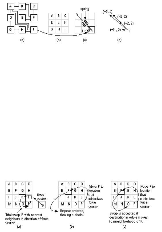
cell j ). If we want, we can also weight the c ij to denote critical connections. Figure 16.27 illustrates the force-directed placement algorithm.
FIGURE 16.27 Force-directed placement. (a) A network with nine logic cells.
(b) We make a grid (one logic cell per bin). (c) Forces are calculated as if springs were attached to the centers of each logic cell for each connection. The two nets connecting logic cells A and I correspond to two springs. (d) The forces are proportional to the spring extensions.
In the definition of connectivity (Section 15.7.1, Measuring Connectivity ) it was pointed out that the network graph does not accurately model connections for nets with more than two terminals. Nets such as clock nets, power nets, and global reset lines have a huge number of terminals. The force-directed placement algorithms usually make special allowances for these situations to prevent the largest nets from snapping all the logic cells together. In fact, without external forces to counteract the pull of the springs between logic cells, the network will collapse to a single point as it settles. An important part of force-directed placement is fixing some of the logic cells in position. Normally ASIC designers use the I/O pads or other external connections to act as anchor points or fixed seeds.
Figure 16.28 illustrates the different kinds of force-directed placement algorithms. The force-directed interchange algorithm uses the force vector to select a pair of logic cells to swap. In force-directed relaxation a chain of logic cells is moved. The force-directed pairwise relaxation algorithm swaps one pair of logic cells at a time.
FIGURE 16.28 Force-directed iterative placement improvement. (a) Force-directed interchange. (b) Force-directed relaxation. (c) Force-directed pairwise relaxation.
We reach a force-directed solution when we minimize the energy of the system, corresponding to minimizing the sum of the squares of the distances separating logic
cells. Force-directed placement algorithms thus also use a quadratic cost function.
16.2.7 Placement Using Simulated
Annealing
The principles of simulated annealing were explained in Section 15.7.8, Simulated Annealing. Because simulated annealing requires so many iterations, it is critical that the placement objectives be easy and fast to calculate. The optimum connection pattern, the MRST, is difficult to calculate. Using the half-perimeter measure ( Section 16.2.3 ) corresponds to minimizing the total interconnect length. Applying simulated annealing to placement, the algorithm is as follows:
1.Select logic cells for a trial interchange, usually at random.
2.Evaluate the objective function E for the new placement.
3.If D E is negative or zero, then exchange the logic cells. If D E is positive, then exchange the logic cells with a probability of exp( D E / T ).
4.Go back to step 1 for a fixed number of times, and then lower the temperature T according to a cooling schedule: T n +1 = 0.9 T n , for example.
Kirkpatrick, Gerlatt, and Vecchi first described the use of simulated annealing applied to VLSI problems [ 1983]. Experience since that time has shown that simulated annealing normally requires the use of a slow cooling schedule and this means long CPU run times [ Sechen, 1988; Wong, Leong, and Liu, 1988]. As a general rule, experiments show that simple min-cut based constructive placement is faster than simulated annealing but that simulated annealing is capable of giving better results at the expense of long computer run times. The iterative improvement methods that we described earlier are capable of giving results as good as simulated annealing, but they use more complex algorithms.
While I am making wild generalizations, I will digress to discuss benchmarks of placement algorithms (or any CAD algorithm that is random). It is important to remember that the results of random methods are themselves random. Suppose the results from two random algorithms, A and B, can each vary by ±10 percent for any chip placement, but both algorithms have the same average performance. If we compare single chip placements by both algorithms, they could falsely show algorithm A to be better than B by up to 20 percent or vice versa. Put another way, if we run enough test cases we will eventually find some for which A is better than B by 20 percent a trick that Ph.D. students and marketing managers both know well. Even single-run evaluations over multiple chips is hardly a fair comparison. The only way to obtain meaningful results is to compare a statistically meaningful number of runs for a statistically meaningful number of chips for each algorithm. This same caution applies to any VLSI algorithm that is random. There was a Design Automation Conference panel session whose theme was Enough of algorithms claiming improvements of 5 %.
16.2.8 Timing-Driven Placement Methods
Minimizing delay is becoming more and more important as a placement objective. There are two main approaches: net based and path based. We know that we can use net weights in our algorithms. The problem is to calculate the weights. One method finds the n most critical paths (using a timing-analysis engine, possibly in the synthesis tool). The net weights might then be the number of times each net appears in this list. The problem with this approach is that as soon as we fix (for example) the first 100 critical nets, suddenly another 200 become critical. This is rather like trying to put worms in a can as soon as we open the lid to put one in, two more pop out.
Another method to find the net weights uses the zero-slack algorithm [ Hauge et al., 1987]. Figure 16.29 shows how this works (all times are in nanoseconds).
Figure 16.29 (a) shows a circuit with primary inputs at which we know the arrival times (this is the original definition, some people use the term actual times ) of each signal. We also know the required times for the primary outputs the points in time at which we want the signals to be valid. We can work forward from the primary inputs and backward from the primary outputs to determine arrival and required times at each input pin for each net. The difference between the required and arrival times at each input pin is the slack time (the time we have to spare). The zero-slack algorithm adds delay to each net until the slacks are zero, as shown in Figure 16.29 (b). The net delays can then be converted to weights or constraints in the placement. Notice that we have assumed that all the gates on a net switch at the same time so that the net delay can be placed at the output of the gate driving the net a rather poor timing model but the best we can use without any routing information.
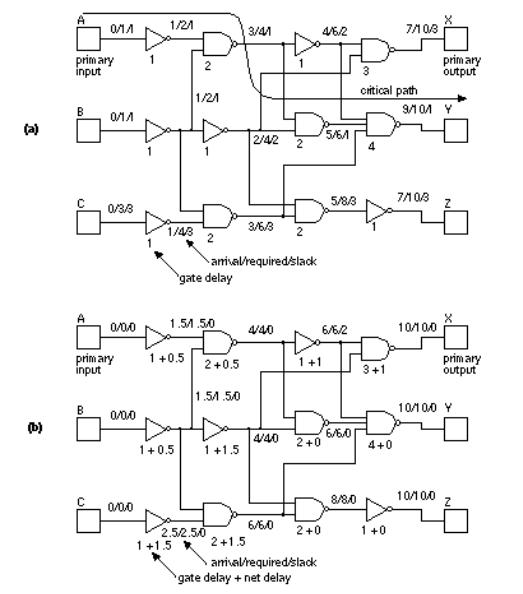
FIGURE 16.29 The zero-slack algorithm. (a) The circuit with no net delays. (b) The zero-slack algorithm adds net delays (at the outputs of each gate, equivalent to increasing the gate delay) to reduce the slack times to zero.
An important point to remember is that adjusting the net weight, even for every net on a chip, does not theoretically make the placement algorithms any more complex we have to deal with the numbers anyway. It does not matter whether the net weight is 1 or 6.6, for example. The practical problem, however, is getting the weight information for each net (usually in the form of timing constraints) from a synthesis tool or timing verifier. These files can easily be hundreds of megabytes in size (see Section 16.4 ).
With the zero-slack algorithm we simplify but overconstrain the problem. For example, we might be able to do a better job by making some nets a little longer than the slack indicates if we can tighten up other nets. What we would really like to do is deal with paths such as the critical path shown in Figure 16.29 (a) and not just nets . Path-based algorithms have been proposed to do this, but they are complex and not all commercial tools have this capability (see, for example, [ Youssef, Lin, and Shragowitz, 1992]).
There is still the question of how to predict path delays between gates with only placement information. Usually we still do not compute a routing tree but use simple approximations to the total net length (such as the half-perimeter measure) and then use this to estimate a net delay (the same to each pin on a net). It is not until the routing step that we can make accurate estimates of the actual interconnect delays.
16.2.9 A Simple Placement Example
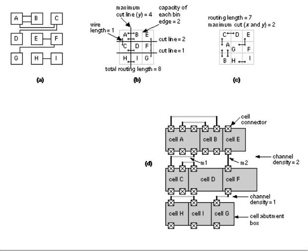
Figure 16.30 shows an example network and placements to illustrate the measures for interconnect length and interconnect congestion. Figure 16.30 (b) and (c) illustrate the meaning of total routing length, the maximum cut line in the x -direction, the maximum cut line in the y -direction, and the maximum density. In this example we have assumed that the logic cells are all the same size, connections can be made to terminals on any side, and the routing channels between each adjacent logic cell have a capacity of 2. Figure 16.30 (d) shows what the completed layout might look like.
FIGURE 16.30 Placement example.
(a) An example network. (b) In this placement, the bin size is equal to the logic cell size and all the logic cells are assumed equal size. (c) An alternative placement with a lower total routing length. (d) A layout that might result from the placement shown in b. The channel densities correspond to the cut-line sizes. Notice that the logic cells are not all the same size (which means there are errors in the interconnect-length estimates we made during placement).
16.4 Information Formats
With the increasing importance of interconnect a great deal of information needs to flow between design tools. There are some de facto standards that we shall look at next. Some of the companies involved are working toward releasing these formats as IEEE standards.
16.4.1 SDF for Floorplanning and Placement
In Section 13.5.6, SDF in Simulation, we discussed the structure and use of the standard delay format ( SDF) to describe gate delay and interconnect delay. We may also use SDF with floorplanning and synthesis tools to back-annotate an interconnect delay. A synthesis tool can use this information to improve the logic structure. Here is a fragment of SDF:
(INSTANCE B) (DELAY (ABSOLUTE
( INTERCONNECT A.INV8.OUT B.DFF1.Q (:0.6:) (:0.6:))))
In this example the rising and falling delay is 60 ps (equal to 0.6 units multiplied by the time scale of 100 ps per unit specified in a TIMESCALE construct that is not shown). The delay is specified between the output port of an inverter with instance name A.INV8 in block A and the Q input port of a D flip-flop (instance name B.DFF1 ) in block B. A '.' (period or fullstop) is set to be the hierarchy divider in another construct that is not shown.
There is another way of specifying interconnect delay using NETDELAY (a short form of the INTERCONNECT construct) as follows:
(TIMESCALE 100ps) (INSTANCE B) (DELAY (ABSOLUTE
( NETDELAY net1 (0.6)))
In this case all delays from an output port to, possibly multiple, input ports have the same value (we can also specify the output port name instead of the net name to identify the net). Alternatively we can lump interconnect delay at an input port:
(TIMESCALE 100ps) (INSTANCE B.DFF1) (DELAY (ABSOLUTE
( PORT CLR (16:18:22) (17:20:25))))
This PORT construct specifies an interconnect delay placed at the input port of a logic cell (in this case the CLR pin of a flip-flop). We do not need to specify the start of a path (as we do for INTERCONNECT ).
We can also use SDF to forward-annotate path delays using timing constraints (there may be hundreds or thousands of these in a file). A synthesis tool can pass this information to the floorplanning and placement steps to allow them to create better layout. SDF describes timing checks using a range of TIMINGCHECK constructs. Here is an example of a single path constraint:
(TIMESCALE 100ps) (INSTANCE B) ( TIMINGCHECK
( PATHCONSTRAINT A.AOI22_1.O B.ND02_34.O (0.8) (0.8)))
This describes a constraint (keyword PATHCONSTRAINT ) for the rising and falling delays between two ports at each end of a path (which may consist of several nets) to be less than 80 ps. Using the SUM construct we can constrain the sum of path delays to be less than a specific value as follows:
(TIMESCALE 100ps) (INSTANCE B) ( TIMINGCHECK
(SUM (AOI22_1.O ND02_34.I1) (ND02_34.O ND02_35.I1) (0.8)))
We can also constrain skew between two paths (in this case to be less than 10 ps) using the DIFF construct:
(TIMESCALE 100ps) (INSTANCE B) (TIMINGCHECK
( DIFF (A.I_1.O B.ND02_1.I1) (A.I_1.O.O B.ND02_2.I1) (0.1)))
In addition we can constrain the skew between a reference signal (normally the clock) and all other ports in an instance (again in this case to be less than 10 ps) using the SKEWCONSTRAINT construct:
(TIMESCALE 100ps) (INSTANCE B) (TIMINGCHECK
( SKEWCONSTRAINT (posedge clk) (0.1)))
At present there is no easy way in SDF to constrain the skew between a reference signal and other signals to be greater than a specified amount.
16.4.2 PDEF
The physical design exchange format ( PDEF ) is a proprietary file format used by Synopsys to describe placement information and the clustering of logic cells. Here is a simple, but complete PDEF file:
(CLUSTERFILE
(PDEFVERSION "1.0")
(DESIGN "myDesign")
(DATE "THU AUG 6 12:00 1995") (VENDOR "ASICS_R_US") (PROGRAM "PDEF_GEN") (VERSION "V2.2")
(DIVIDER .)
( CLUSTER (NAME "ROOT") (WIRE_LOAD "10mm x 10mm") (UTILIZATION 50.0) (MAX_UTILIZATION 60.0) (X_BOUNDS 100 1000) (Y_BOUNDS 100 1000) (CLUSTER (NAME "LEAF_1") (WIRE_LOAD "50k gates") (UTILIZATION 50.0) (MAX_UTILIZATION 60.0) (X_BOUNDS 100 500) (Y_BOUNDS 100 200)
(CELL (NAME L1.RAM01) (CELL (NAME L1.ALU01)
)
)
)
This file describes two clusters:
●ROOT , which is the top-level (the whole chip). The file describes the size ( x - and y -bounds), current and maximum area utilization (i.e., leaving space for interconnect), and the name of the wire-load table, '
10mm x 10mm ', to use for this block, chosen because the chip is expected to be about 10 mm on a side.
●LEAF_1 , a block below the top level in the hierarchy. This block is to use predicted capacitances from a wire-load table named '50k gates' (chosen

because we know there are roughly 50 k-gate in this block). The LEAF_1 block contains two logic cells: L1.RAM01 and L1.ALU01 .
16.4.3 LEF and DEF
The library exchange format ( LEF ) and design exchange format ( DEF ) are both proprietary formats originated by Tangent in the TanCell and TanGate place-and-route tools which were bought by Cadence and now known as Cell3 Ensemble and Gate Ensemble respectively. These tools, and their derivatives, are so widely used that these formats have become a de facto standard. LEF is used to define an IC process and a logic cell library. For example, you would use LEF to describe a gate array: the base cells, the legal sites for base cells, the logic macros with their size and connectivity information, the interconnect layers and other information to set up the database that the physical design tools need. You would use DEF to describe all the physical aspects of a particular chip design including the netlist and physical location of cells on the chip. For example, if you had a complete placement from a floorplanning tool and wanted to exchange this information with Cadence Gate Ensemble or Cell3 Ensemble, you would use DEF.