

6.3 DC Input
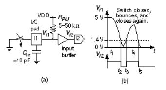
Suppose we have a pushbutton switch connected to the input of an FPGA as shown in Figure 6.11 (a). Most FPGA input pads are directly connected to a buffer. We need to ensure that the input of this buffer never floats to a voltage between valid logic levels (which could cause both n -channel and p -channel transistors in the buffer to turn on, leading to oscillation or excessive power dissipation) and so we use the optional pull-up resistor (usually about 100 k W ) that is available on many FPGAs (we could also connect a 1 k W pull-up or pull-down resistor externally).
Contacts may bounce as a switch is operated ( Figure 6.11 b). In the case of a Xilinx XC4000 the effective pull-up resistance is 5 50 k W (since the specified pull-up current is between 0.2 and 2.0 mA) and forms an RC time constant with the parasitic capacitance of the input pad and the external circuit. This time constant (typically hundreds of nanoseconds) will normally be much less than the time over which the contacts bounce (typically many milliseconds). The buffer output may thus be a series of pulses extending for several milliseconds. It is up to you to deal with this in your logic. For example, you may want to debounce the waveform in Figure 6.11 (b) using an SR flip-flop.
FIGURE 6.11 A switch input. (a) A pushbutton switch connected to an input buffer with a pull-up resistor.
(b) As the switch bounces several pulses may be generated.
A bouncing switch may create a noisy waveform in the time domain, we may also have noise in the voltage level of our input signal. The Schmitt-trigger inverter in Figure 6.12
(a) has a lower switching threshold of 2 V and an upper switching threshold of 3 V. The difference between these thresholds is the hysteresis , equal to 1 V in this case. If we apply the noisy waveform shown in Figure 6.12 (b) to an inverter with no hysteresis, there will be a glitch at the output, as shown in Figure 6.12 (c). As long as the noise on the waveform does not exceed the hysteresis, the Schmitt-trigger inverter will produce the glitch-free output of Figure 6.12 (d).
Most FPGA input buffers have a small hysteresis (the 200 mV that Xilinx uses is a typical figure) centered around 1.4 V (for compatibility with TTL), as shown in
Figure 6.12 (e). Notice that the drawing inside the symbol for a Schmitt trigger looks like the transfer characteristic for a buffer, but is backward for an inverter. Hysteresis in the input buffer also helps prevent oscillation and noise problems with inputs that have slow
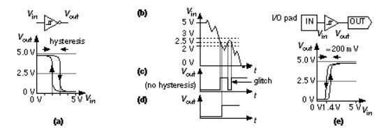
rise times, though most FPGA manufacturers still have a restriction that input signals must have a rise time faster than several hundred nanoseconds.
FIGURE 6.12 DC input. (a) A Schmitt-trigger inverter. (b) A noisy input signal.
(c) Output from an inverter with no hysteresis. (d) Hysteresis helps prevent glitches.
(e) A typical FPGA input buffer with a hysteresis of 200 mV centered around a threshold of 1.4 V.
6.3.1 Noise Margins
Figure 6.13 (a) and (b) show the worst-case DC transfer characteristics of a CMOS inverter. Figure 6.13 (a) shows a situation in which the process and device sizes create the lowest possible switching threshold. We define the maximum voltage that will be recognized as a '0' as the point at which the gain ( V out / V in ) of the inverter is 1. This point is V ILmax = 1V in the example shown in Figure 6.13 (a). This means that any input voltage that is lower than 1V will definitely be recognized as a '0', even with the most unfavorable inverter characteristics. At the other worst-case extreme we define the minimum voltage that will be recognized as a '1' as V IHmin = 3.5V (for the example in Figure 6.13 b).
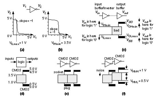
FIGURE 6.13 Noise margins. (a) Transfer characteristics of a CMOS inverter with the lowest switching threshold. (b) The highest switching threshold. (c) A graphical representation of CMOS logic thresholds. (d) Logic thresholds at the inputs and outputs of a logic gate or an ASIC. (e) The switching thresholds viewed as a plug and socket.
(f) CMOS plugs fit CMOS sockets and the clearances are the noise margins.
Figure 6.13 (c) depicts the following relationships between the various voltage levels at the inputs and outputs of a logic gate:
●A logic '1' output must be between V OHmin and V DD .
●A logic '0' output must be between V SS and V OLmax .
●A logic '1' input must be above the high-level input voltage , V IHmin .
●A logic '0' input must be below the low-level input voltage , V ILmax .
●Clamp diodes prevent an input exceeding V DD or going lower than V SS .
The voltages, V OHmin , V OLmax , V IHmin , and V ILmax , are the logic thresholds for a technology. A logic signal outside the areas bounded by these logic thresholds is bad an unrecognizable logic level in an electronic no-man s land. Figure 6.13 (d) shows typical logic thresholds for a CMOS-compatible FPGA. The V IHmin and V ILmax logic thresholds come from measurements in Figure 6.13 (a) and (b) and V OHmin and V OLmax come from the measurements shown in Figure 6.2 (c).
Figure 6.13 (d) illustrates how logic thresholds form a plug and socket for any gate, group of gates, or even a chip. If a plug fits a socket, we can connect the two components together and they will have compatible logic levels. For example, Figure 6.13 (e) shows that we can connect two CMOS gates or chips together.
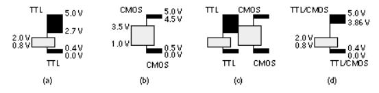
FIGURE 6.14 TTL and CMOS logic thresholds. (a) TTL logic thresholds. (b) Typical CMOS logic thresholds. (c) A TTL plug will not fit in a CMOS socket. (d) Raising V OHmin solves the problem.
Figure 6.13 (f) shows that we can even add some noise that shifts the input levels and the plug will still fit into the socket. In fact, we can shift the plug down by exactly V OHmin V IHmin (4.5 3.5 = 1 V) and still maintain a valid '1'. We can shift the plug up by V ILmaxV OLmax (1.0 0.5 = 0.5 V) and still maintain a valid '0'. These clearances between plug and socket are the noise margins :
V NMH = V OHmin V IHmin and V NML = V ILmax V OLmax . (6.1)
For two logic systems to be compatible, the plug must fit the socket. This requires both the high-level noise margin (V NMH ) and the low-level noise margin (V NML ) to be positive. We also want both noise margins to be as large as possible to give us maximum immunity from noise and other problems at an interface.
Figure 6.14 (a) and (b) show the logic thresholds for TTL together with typical CMOS logic thresholds. Figure 6.14 (c) shows the problem with trying to plug a TTL chip into a CMOS input level the lowest permissible TTL output level, V OHmin = 2.7 V, is too low to be recognized as a logic '1' by the CMOS input. This is fixed by most FPGA manufacturers by raising V OHmin to around 3.8 4.0 V ( Figure 6.14 d). Table 6.1 lists the logic thresholds for several FPGAs.
6.3.2 Mixed-Voltage Systems
To reduce power consumption and allow CMOS logic to be scaled below 0.5 m m it is necessary to reduce the power supply voltage below 5 V. The JEDEC 8 [ JEDEC I/O] series of standards sets the next lower supply voltage as 3.3 ± 0.3 V. Figure 6.15 (a) and
(b) shows that the 3 V CMOS I/O logic-thresholds can be made compatible with 5 V systems. Some FPGAs can operate on both 3 V and 5 V supplies, typically using one voltage for internal (or core) logic, V DDint and another for the I/O circuits, V DDI/O ( Figure 6.15 c).
TABLE 6.1 FPGA logic thresholds. |
|
|
I/O options Input levels |
Output levels (high |
Output levels (low |
|
current) |
current) |
V IH V IL |
V OH I OH V OL I OL |
V OH I OH VOL I OL |
Input Output |
|
|
(min) (max) (min) (max) (max) (max) (min) (max) (max) (max)
XC3000 1 TTL |
|
2.0 |
0.8 |
3.86 |
4.0 |
0.40 |
4.0 |
|
|
|
|
CMOS |
|
3.85 |
0.9 3 |
3.86 |
4.0 |
0.40 |
4.0 |
|
|
|
|
|
|
2 |
|
|
|
|
|
|
|
|
|
XC3000L |
|
2.0 |
0.8 |
2.40 |
4.0 |
0.40 |
4.0 |
2.80 |
0.1 |
0.2 |
0.1 |
|
|
|
|
|
|
|
|
4 |
|
|
|
XC4000 5 |
|
2.0 |
0.8 |
2.40 |
4.0 |
0.40 |
12.0 |
|
|
|
|
XC4000H TTL |
TTL |
2.0 |
0.8 |
2.40 |
4.0 |
0.50 |
24.0 |
|
|
|
|
6 |
|
|
|
|
|
|
|
|
|
|
|
CMOS CMOS |
3.85 |
0.9 3 |
4.00 |
1.0 |
0.50 |
24.0 |
|
|
|
|
|
|
|
2 |
|
7 |
|
|
|
|
|
|
|
XC8100 8 TTL |
R |
2.0 |
0.8 |
3.86 |
4.0 |
0.50 |
24.0 |
|
|
|
|
CMOS C |
3.85 |
0.9 3 |
3.86 |
4.0 |
0.40 |
4.0 |
|
|
|
|
|
|
|
2 |
|
|
|
|
|
|
|
|
|
ACT 2/3 |
|
2.0 |
0.8 |
2.4 |
8.0 |
0.50 |
12.0 |
3.84 |
4.0 |
0.33 |
6.0 |
FLEX10k |
3V/5V |
2.0 |
0.8 |
2.4 |
4.0 |
0.45 |
12.0 |
|
|
|
|
9 |
|
|
|
|
|||||||
|
|
|
|
|
|
|
|
|
|
|
|
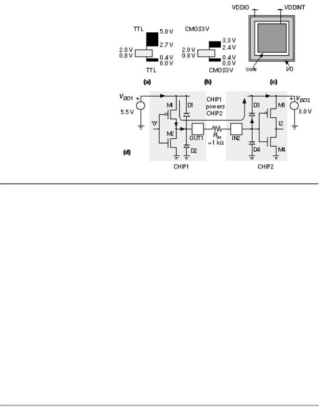
There is one problem when we mix 3 V and 5 V supplies that is shown in Figure 6.15 (d). If we apply a voltage to a chip input that exceeds the power supply of a chip, it is possible to power a chip inadvertently through the clamp diodes. In the worst case this may cause a voltage as high as 2.5 V (= 5.5 V 3.0 V) to appear across the clamp diode, which will cause a very large current (several hundred milliamperes) to flow. One way to prevent damage is to include a series resistor between the chips, typically around 1 k W . This solution does not work for all chips in all systems. A difficult problem in ASIC I/O design is constructing 5 V-tolerant I/O . Most solutions may never surface (there is little point in patenting a solution to a problem that will go away before the patent is granted).
Similar problems can arise in several other situations:
●when you connect two ASICs with different 5 V supplies;
●when you power down one ASIC in a system but not another, or one ASIC powers down faster than another;
●on system power-up or system reset.
FIGURE 6.15
Mixed-voltage systems.
(a)TTL levels.
(b)Low-voltage CMOS levels. (c) A mixed-voltage ASIC.
(d)A problem when connecting two chips with different supply voltages caused by the input clamp diodes.
1.XC2000, XC3000/A have identical thresholds. XC3100/A thresholds are identical to XC3000 except for ±8 mA source sink current. XC5200 thresholds are identical to XC3100A.
2.Defined as 0.7 V DD , calculated with V DD max = 5.5 V.
3.Defined as 0.2 V DD , calculated with V DD min = 4.5 V.
4.Defined as V DD 0.2 V, calculated with V DD min = 3.0 V.
5.XC4000, XC4000A have identical I/O thresholds except XC4000A has 24 mA sink current.
6.XC4000H/E have identical I/O thresholds except XC4000E has 12 mA sink current. Options are independent.
7.Defined as VDD 0.5 V, calculated with VDD min = 4.5 V.
8.Input and output options are independent.
9.MAX 9000 has identical thresholds to FLEX 10k.
Note: All voltages in volts, all currents in milliamperes.