

14.3 Faults
Fabrication of an ASIC is a complicated process requiring hundreds of processing steps. Problems may introduce a defect that in turn may introduce a fault (Sabnis [ 1990] describes defect mechanisms ). Any problem during fabrication may prevent a transistor from working and may break or join interconnections. Two common types of defects occur in metallization [ Rao, 1993]: either underetching the metal (a problem between long, closely spaced lines), which results in a bridge or short circuit ( shorts ) between adjacent lines, or overetching the metal and causing breaks or open circuits ( opens ). Defects may also arise after chip fabrication is complete while testing the wafer, cutting the die from the wafer, or mounting the die in a package. Wafer probing, wafer saw, die attach, wire bonding, and the intermediate handling steps each have their own defect and failure mechanisms. Many different materials are involved in the packaging process that have different mechanical, electrical, and thermal properties, and these differences can cause defects due to corrosion, stress, adhesion failure, cracking, and peeling. Yield loss also occurs from human error using the wrong mask, incorrectly setting the implant dose as well as from physical sources: contaminated chemicals, dirty etch sinks, or a troublesome process step. It is possible to repeat or rework some of the reversible steps (a lithography step, for example but not etching) if there are problems. However, reliance on rework indicates a poorly controlled process.
14.3.1 Reliability
It is possible for defects to be nonfatal but to cause failures early in the life of a product. We call this infant mortality . Most products follow the same kinds of trend for failures as a function of life. Failure rates decrease rapidly to a low value that remains steady until the end of life when failure rates increase again; this is called a bathtub curve . The end of a product lifetime is determined by various wearout mechanisms (usually these are controlled by an exponential energy process). Some of the most important wearout mechanisms in ASICs are hot-electron wearout, electromigration, and the failure of antifuses in FPGAs.
We can catch some of the products that are susceptible to early failure using burn-in . Many failure mechanisms have a failure rate proportional to exp ( E a /kT). This is the Arrhenius equation , where E a is a known activation energy (k is Boltzmann s
constant, 8.62 ¥ 10 5 eVK -1 , and T the absolute temperature). Operating an ASIC at an elevated temperature accelerates this type of failure mechanism. Depending on the physics of the failure mechanism, additional stresses, such as elevated current or voltage, may also accelerate failures. The longer and harsher the burn-in conditions, the more likely we are to find problems, but the more costly the process and the more
costly the parts.
We can measure the overall reliability of any product using the mean time between failures ( MTBF ) for a repairable product or mean time to failure ( MTTF ) for a fatal failure. We also use failures in time ( FITs ) where 1 FIT equals a single failure in 10 9 hours. We can sum the FITs for all the components in a product to determine an overall measure for the product reliability. Suppose we have a system with the following components:
●Microprocessor (standard part) 5 FITs
●100 TTL parts, 50 parts at 10 FITs, 50 parts at 15 FITs
●100 RAM chips, 6 FITs
The overall failure rate for this system is 5 + 50 ¥ 10 + 50 ¥ 15 + 100 ¥ 6 = 1855 FITs. Suppose we could reduce the component count using ASICs to the following:
●Microprocessor (custom) 7 FITs
●9 ASICs, 10 FITs
●5 SIMMs, 15 FITs
The failure rate is now 10 + 9 ¥ 10 + 5 ¥ 15 = 175 FITs, or about an order of magnitude lower. This is the rationale behind the Sun SparcStation 1 design described in Section 1.3 , Case Study .
14.3.2 Fault Models
Table 14.6 shows some of the causes of faults. The first column shows the fault levelwhether the fault occurs in the logic gates on the chip or in the package. The second column describes the physical fault . There are too many of these and we need a way to reduce and simplify their effects by using a fault model.
There are several types of fault model . First, we simplify things by mapping from a physical fault to a logical fault . Next, we distinguish between those logical faults that degrade the ASIC performance and those faults that are fatal and stop the ASIC from working at all. There are three kinds of logical faults in Table 14.6 : a degradation fault, an open-circuit fault, and a short-circuit fault.
TABLE 14.6 Mapping physical faults to logical faults.
Logical fault
Fault |
Physical fault |
Degradation fault Open-circuit fault Short-circuit fault |
||
level |
||||
|
|
|
||
Chip |
|
|
|
|
|
Leakage or short |
|
|
|
|
between package |
" |
" |
|
|
leads |
|
|
|
Broken, misaligned,
"
or poor wire bonding
14.3.3 Physical Fults
Figure 14.11 shows the following examples of physical faults in a logic cell:
FIGURE 14.11 Defects and physical faults. Many types of defects occur during fabrication. Defects can be of any size and on any layer. Only a few small sample defects are shown here using a typical standard cell as an example. Defect density for a modern CMOS process is of the order of 1 cm 2 or less across a whole wafer. The logic cell shown here is approximately 64 ¥ 32 l 2 , or 250 m m 2 for a l = 0.25 m m process. We would thus have to examine approximately 1 cm 2 /250 m m 2 or 400,000 such logic cells to find a single defect.
●F1 is a short between m1 lines and connects node n1 to VSS.
●F2 is an open on the poly layer and disconnects the gate of transistor t1 from the rest of the circuit.
●F3 is an open on the poly layer and disconnects the gate of transistor t3 from the rest of the circuit.
●F4 is a short on the poly layer and connects the gate of transistor t4 to the gate of transistor t5.
●F5 is an open on m1 and disconnects node n4 from the output Z1.
●F6 is a short on m1 and connects nodes p5 and p6.
●F7 is a nonfatal defect that causes necking on m1.
Once we have reduced the large number of physical faults to fewer logical faults, we need a model to predict their effect. The most common model is the stuck-at fault model .
14.3.4 Stuck-at Fault Model
The single stuck-at fault ( SSF ) model assumes that there is just one fault in the logic we are testing. We use a single stuck-at fault model because a multiple stuck-at fault model that could handle several faults in the logic at the same time is too complicated to implement. We hope that any multiple faults are caught by single stuck-at fault tests [Agarwal and Fung, 1981; Hughes and McCluskey, 1986]. In practice this seems to be true.
There are other fault models. For example, we can assume that faults are located in the transistors using a stuck-on fault and stuck-open fault (or stuck-off fault ). Fault models such as these are more realistic in that they more closely model the actual physical faults. However, in practice the simple SSF model has been found to workand work well. We shall concentrate on the SSF model.
In the SSF model we further assume that the effect of the physical fault (whatever it may be) is to create only two kinds of logical fault. The two types of logical faults or stuck-at faults are: a stuck-at-1 fault (abbreviated to SA1 or s@1) and a stuck-at-0 fault ( SA0 or s@0). We say that we place faults ( inject faults , seed faults , or apply faults ) on a node (or net), on an input of a circuit, or on an output of a circuit. The location at which we place the fault is the fault origin .
A net fault forces all the logic cell inputs that the net drives to a logic '1' or '0' . An input fault attached to a logic cell input forces the logic cell input to a '1' or '0' , but does not affect other logic cell inputs on the same net. An output fault attached to the output of a logic cell can have different strengths. If an output fault is a supply-strength fault (or rail-strength fault) the logic-cell output node and every other node on that net is forced to a '1' or '0' as if all these nodes were connected to one of the supply rails. An alternative assigns the same strength to the output fault as the drive strength of the logic cell. This allows contention between outputs on a net driving the same node. There is no standard method of handling output-fault strength , and no standard for using types of stuck-at faults. Usually we do not inject net faults; instead we inject only input faults and output faults. Some people use the term node fault but in different ways to mean either a net fault, input fault, or output fault.
We usually inject stuck-at faults to the inputs and outputs, the pins, of logic cells (AND gates, OR gates, flip-flops, and so on). We do not inject faults to the internal nodes of a flip-flop, for example. We call this a pin-fault model and say the fault level is at the structural level , gate level, or cell level. We could apply faults to the internal logic of a logic cell (such as a flip-flop) and (the fault level would then be at the transistor level or switch level. We do not use transistor-level or switch-level fault models because there is often no need. From experience, but not from any theoretical reason, it turns out that using a fault model that applies faults at the logic-cell level is sufficient to catch the bad chips in a production test.
When a fault changes the circuit behavior, the change is called the fault effect . Fault effects travel through the circuit to other logic cells causing other fault effects. This phenomenon is fault propagation . If the fault level is at the structural level, the phenomenon is structural fault propagation . If we have one or more large functional blocks in a design, we want to apply faults to the functional blocks only at the inputs and outputs of the blocks. We do not want to place (or cannot place) faults inside the blocks, but we do want faults to propagate through the blocks. This is behavioral fault propagation .
Designers adjust the fault level to the appropriate level at which they think there may be faults. Suppose we are performing a fault simulation on a board and we have already tested the chips. Then we might set the fault level to the chip level, placing faults only at the chip pins. For ASICs we use the logic-cell level. You have to be careful, though, if you mix behavioral level and structural level models in a mixed-level fault simulation . You need to be sure that the behavioral models propagates faults correctly. In particular, if the behavioral model responds to faults on its inputs by propagating too many unknown 'X' values to its outputs, this will decrease the fault coverage, because the model is hiding the logic beyond it.
14.3.5 Logical Faults
Figure 14.12 and the following list show how the defects and physical faults of Figure 14.11 translate to logical faults (not all physical faults translate to logical faultsmost do not):
●F1 translates to node n1 being stuck at 0, equivalent to A1 being stuck at 1.
●F2 will probably result in node n1 remaining high, equivalent to A1 being stuck at 0.
●F3 will affect half of the n -channel pull-down stack and may result in a degradation fault, depending on what happens to the floating gate of T3. The cell will still work, but the fall time at the output will approximately double. A fault such as this in the middle of a chain of logic is extremely hard to detect.
●F4 is a bridging fault whose effect depends on the relative strength of the transistors driving this node. The fault effect is not well modeled by a stuck-at fault model.
●F5 completely disables half of the n -channel pulldown stack and will result in a degradation fault.
●F6 shorts the output node to VDD and is equivalent to Z1 stuck at 1.
●Fault F7 could result in infant mortality. If this line did break due to electromigration the cell could no longer pull Z1 up to VDD. This would translate to a Z1 stuck at 0. This fault would probably be fatal and stop the ASIC working.
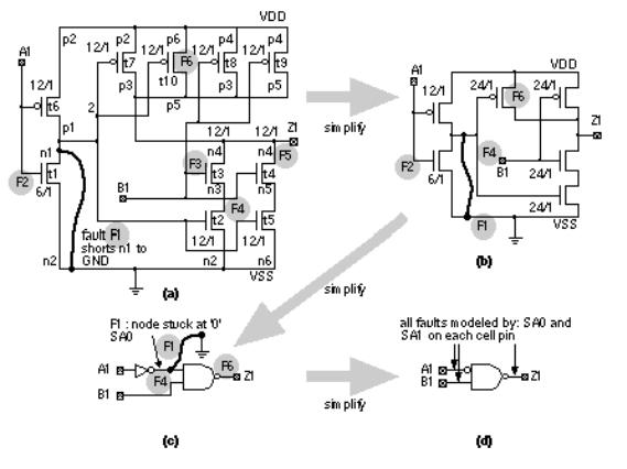
FIGURE 14.12 Fault models. (a) Physical faults at the layout level (problems during fabrication) shown in Figure 14.11 translate to electrical problems on the detailed circuit schematic. The location and effect of fault F1 is shown. The locations of the other fault examples from Figure 14.11 (F2 F6) are shown, but not their effect. (b) We can translate some of these faults to the simplified transistor schematic. (c) Only a few of the physical faults still remain in a gate-level fault model of the logic cell. (d) Finally at the functional-level fault model of a logic cell, we abandon the connection between physical and logical faults and model all faults by stuck-at faults. This is a very poor model of the physical reality, but it works well in practice.
14.3.6 IDDQ Test
When they receive a prototype ASIC, experienced designers measure the resistance between VDD and GND pins. Providing there is not a short between VDD and GND, they connect the power supplies and measure the power-supply current. From experience they know that a supply current of more than a few milliamperes indicates a bad chip. This is exactly what we want in production test: Find the bad chips quickly, get them off the tester, and save expensive tester time. An IDDQ (IDD stands for the supply current, and Q stands for quiescent) test is one of the first production tests applied to a chip on the tester, after the chip logic has been initialized [ Gulati and Hawkins, 1993; Rajsuman, 1994]. High supply current can result from bridging faults that we described in Section 14.3.2 . For example, the bridging fault F4 in Figure 14.11 and Figure 14.12 would cause excessive IDDQ if node n1 and input B1 are being driven to opposite values.
14.3.7 Fault Collapsing
Figure 14.13 (a) shows a test for a stuck-at-1 output of a two-input NAND gate. Figure 14.13 (b) shows tests for other stuck-at faults. We assume that the NAND gate still works correctly in the bad circuit (also called the faulty circuit or faulty machine ) even if we have an input fault. The input fault on a logic cell is presumed to arise either from a fault from a preceding logic cell or a fault on the connection to the input.
Stuck-at faults attached to different points in a circuit may produce identical fault effects. Using fault collapsing we can group these equivalent faults (or indistinguishable faults ) into a fault-equivalence class . To save time we need only consider one fault, called the prime fault or representative fault , from a fault-equivalence class. For example, Figure 14.13 (a) and (b) show that a stuck-at-0 input and a stuck-at-1 output are equivalent faults for a two-input NAND gate. We only need to check for one fault, Z1 (output stuck at 1), to catch any of the equivalent faults.
Suppose that any of the tests that detect a fault B also detects fault A, but only some of the tests for fault A also detect fault B. W say A is a dominant fault , or that fault A dominates fault B (this the definition of fault dominance that we shall use, some texts say fault B dominates fault A in this situation). Clearly to reduce the number of tests using dominant fault collapsing we will pick the test for fault B. For example,
Figure 14.13 (c) shows that the output stuck at 0 dominates either input stuck at 1 for a two-input NAND. By testing for fault A1, we automatically detect the fault Z1. Confusion over dominance arises because of the difference between focusing on faults ( Figure 14.13 d) or test vectors ( Figure 14.13 e).
Figure 14.13 (f) shows the six stuck-at faults for a two-input NAND gate. We can place SA1 or SA0 on each of the two input pins (four faults in total) and SA1 or SA0 on the output pins. Using fault equivalence ( Figure 14.13 g) we can collapse six faults to four: SA1 on each input, and SA1 or SA0 on the output. Using fault dominance ( Figure 14.13 h) we can collapse six faults to three. There is no way to tell the difference between equivalent faults, but if we use dominant fault collapsing we may lose information about the fault location.
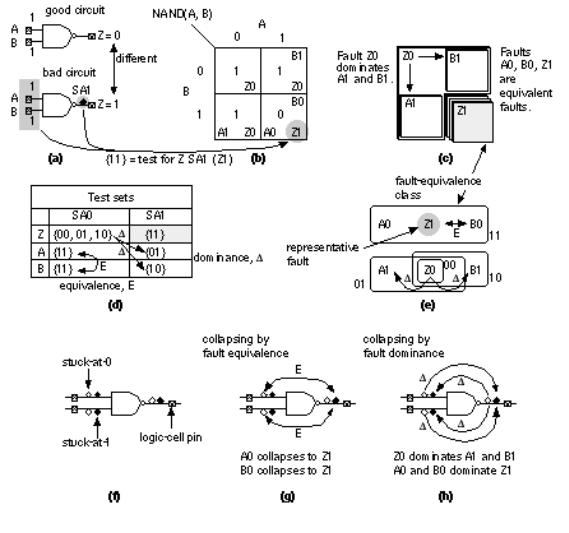
FIGURE 14.13 Fault dominance and fault equivalence. (a) We can test for fault Z0 (Z stuck at 0) by applying a test vector that makes the bad (faulty) circuit produce a different output than the good circuit. (b) Some test vectors provide tests for more than one fault. (c) A test for A stuck at 1 (A1) will also test for Z stuck at 0; Z0 dominates A1. The fault effects of faults: A0, B0 and Z1 are the same. These faults are equivalent. (d) There are six sets of input vectors that test for the six stuck-at faults. (e) We only need to choose a subset of all test vectors that test for all faults.
(f) The six stuck-at faults for a two-input NAND logic cell. (g) Using fault equivalence we can collapse six faults to four. (h) Using fault dominance we can collapse six faults to three.
14.3.8 Fault-Collapsing Example
Figure 14.14 shows an example of fault collapsing. Using the properties of logic cells to reduce the number of faults that we need to consider is called gate collapsing . We can also use node collapsing by examining the effect of faults on the same node.
Consider two inverters in series. An output fault on the first inverter collapses with the node fault on the net connecting the inverters. We can collapse the node fault in turn with the input fault of the second inverter. The details of fault collapsing depends on whether the simulator uses net or pin faults, the fanin and fanout of nodes, and the output fault-strength model used.
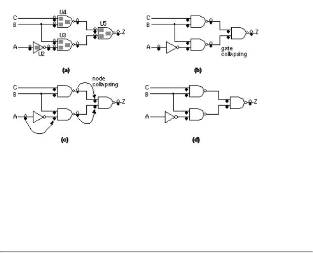
FIGURE 14.14 Fault collapsing for A'B + BC. (a) A pin-fault model. Each pin has stuck-at-0 and stuck-at-1 faults. (b) Using fault equivalence the pin faults at the input pins and output pins of logic cells are collapsed. This is gate collapsing. (c) We can reduce the number of faults we need to consider further by collapsing equivalent faults on nodes and between logic cells. This is node collapsing. (d) The final circuit has eight stuck-at faults (reduced from the 22 original faults). If we wished to use fault dominance we could also eliminate the stuck-at-0 fault on Z. Notice that in a pin-fault model we cannot collapse the faults U4.A1.SA1 and U3.A2.SA1 even though they are on the same net.