


11.16 Bibliography
The IEEE Verilog LRM [1995] is less intimidating than the IEEE VHDL LRM, because it is based on the OVI LRM, which in turn was based on the Verilog-XL simulator reference manual. Thus it has more of a "User's Guide" flavor and is required reading for serious Verilog users. It is the only source for detailed information on the PLI.
Phil Moorby was one of the original architects of the Verilog language. The Thomas and Moorby text is a good introduction to Verilog [1991]. The code examples from this book can be obtained from the World Wide Web. Palnitkar's book includes an example of the use of the PLI routines [1996].
Open Verilog International (OVI) has a Web site maintained by Chronologic ( http://www.chronologic.com/ovi ) with membership information and addresses and an ftp site maintained by META-Software ( ftp://ftp.metasw.com in /pub/OVI/ ). OVI sells reference material, including proceedings from the International Verilog HDL Conference.
The newsgroup comp.lang.verilog (with a FAQ--frequently asked questions) is accessible from a number of online sources. The FAQ includes a list of reference materials and book reviews. Cray Research maintained an archive for comp.lang.verilog going back to 1993 but this was lost in January 1997 and is still currently unavailable. Cadence has a discussion group at talkverilog@cadence.com . Wellspring Solutions offers VeriWell, a no-cost, limited capability, Verilog simulator for UNIX, PC, and Macintosh platforms.
There is a free, "copylefted" Verilog simulator, vbs , written by Jimen Ching and Lay Hoon Tho as part of their Master's theses at the University of Hawaii, which is part of the comp.lang.verilog archive. The package includes explanations of the mechanics of a digital event-driven simulator, including event queues and time wheels.
More technical references are included as part of Appendix B.
11.17 References
IEEE Std 1364-95, Verilog LRM. 1995. The Institute of Electrical and Electronics Engineers. Available from The Institute of Electrical and Electronics Engineers, Inc., 345 East 47th Street, New York, NY 10017 USA. [cited on
p. 479]
Palnitkar, S. 1996. Verilog HDL: A Guide to Digital Design and Synthesis. Upper Saddle River, NJ: Prentice-Hall, 396 p. ISBN 0-13-451675-3.
Thomas, D. E., and P. Moorby. 1991. The Verilog Hardware Description Language. 1st ed. Dordrecht, Netherlands: Kluwer, 223 p. ISBN 0-7923-9126-8, TK7885.7.T48 (1st ed.). ISBN 0-7923-9523-9 (2nd ed.).

`timescale |
1ns/1ns |
|
|
|
module counter; |
|
|
|
|
reg clock; |
// declare reg data type for |
the clock |
||
integer |
count; |
// declare integer data type |
for the count |
|
initial // |
initialize things - this executes once |
at start |
||
begin |
|
|
|
|
clock = 0; count = 0; |
// initialize signals |
|||
#340 |
$finish; |
|
// finish after 340 time ticks |
|
end
/* an always statement to generate the clock, only one statement follows the always so we don't need a begin and an end */
always
#10 clock = ~ clock; // delay is set to half the clock cycle
/* an always statement to do the counting, runs at the same time (concurrently) as the other always statement */
always begin
//wait here until the clock goes from 1 to 0 @ (negedge clock);
//now handle the counting
if (count == 7) count = 0;
else
count = count + 1;
$display("time = ",$time," count = ", count);
end endmodule
module identifiers;
/* multi-line comments in Verilog
look like C comments and // is OK in here */ // single-line comment in Verilog
reg legal_identifier,two__underscores;
reg _OK,OK_,OK_$,OK_123,CASE_SENSITIVE, case_sensitive;
reg \/clock ,\a*b ; |
// white_space after escaped identifier |
//reg $_BAD,123_BAD; |
// bad names even if we declare them! |
initial begin |
|
legal_identifier =0; |
// embedded underscores are OK |
two__underscores =0; |
// even two underscores in a row |
_OK = 0; |
// identifiers can start with underscore |
OK_ = 0; |
// and end with underscore |
OK$ = 0; |
// $ sign is OK: beware foreign keyboards |
OK_123 =0; |
// embedded digits are OK |
CASE_SENSITIVE =0; |
// Verilog is case-sensitive |
case_sensitive =1; |
|
\/clock =0; |
// escaped identifier with \ breaks rules |
\a*b =0; |
// but be careful! watch the spaces |
$display("Variable CASE_SENSITIVE= %d",CASE_SENSITIVE); $display("Variable case_sensitive= %d",case_sensitive); $display("Variable \/clock = %d",\/clock ); $display("Variable \\a*b = %d",\a*b );
end endmodule
module declarations_1;
wire pwr_good,pwr_on,pwr_stable; // Explicitly declare wires
integer i; |
// 32-bit, signed (2's complement) |
|
time t; |
// 64-bit, unsigned, behaves like a 64-bit reg |
|
event e; |
// Declare an event data type |
|
real r; |
// Real data type of implementation defined size |
|
// assign statement continuously drives a wire... |
|
|
assign pwr_stable = 1'b1; assign pwr_on = 1; |
// 1 or 1'b1 |
|
assign pwr_good = pwr_on & pwr_stable; |
|
|
initial begin |
|
|
i = 123.456; |
// There must be a digit on either side |
|

r = |
123456e-3; |
// of the decimal point |
if it is present. |
|
t = |
123456e-3; |
// Time is |
rounded to 1 |
second by default. |
$display("i=%0g",i," t=%6.2f",t," r=%f",r); |
|
|
||
#2 $display("TIME=%0d",$time," ON=",pwr_on, " STABLE=",pwr_stable," GOOD=",pwr_good);
$finish; end endmodule
module declarations_2; reg Q, Clk; wire D;
//drive the wire (D) assign D = 1;
//at +ve clock edge assign the value of wire D to the reg Q: always @(posedge Clk) Q = D;
initial Clk = 0; always #10 Clk = ~ Clk; initial begin #50; $finish; end
always begin
$display("T=%2g", $time," D=",D," Clk=",Clk," Q=",Q); #10; end endmodule
module declarations_3; |
|
|
reg a,b,c,d,e; |
|
|
initial begin |
|
|
#10; a=0;b=0;c=0;d=0; |
#10; |
a=0;b=1;c=1;d=0; |
#10; a=0;b=0;c=1;d=1; |
#10; |
$stop; |
end
always begin
@(a or b or c or d) e = (a|b)&(c|d); $display("T=%0g",$time," e=",e);
end endmodule
module declarations_4; |
|
|
|
wire Data; |
// |
a scalar net of |
type wire |
wire [31:0] ABus, DBus; |
// |
two 32-bit wide |
vector wires... |
//DBus[31] = left-most = most-significant bit = msb
//DBus[0] = right-most = least-significant bit = lsb
//Notice the size declaration precedes the names
//wire [31:0] TheBus, [15:0] BigBus; // illegal
reg [3:0] vector; |
// a 4-bit vector register |
reg [4:7] nibble; |
// msb index < lsb index |
integer i; |
|
initial begin |
|
i = 1; |
|
vector = 'b1010; |
// vector without an index |
nibble = vector; |
// this is OK too |
#1; $display("T=%0g",$time," vector=", vector," nibble=", nibble); |
|
#2; $display("T=%0g",$time," Bus=%b",DBus[15:0]); |
|
end |
|
assign DBus [1] = 1; |
// this is a bit-select |
assign DBus [3:0] = 'b1111; |
// this is a part-select |
// assign DBus [0:3] = 'b1111; |
// illegal - wrong direction |
endmodule |
|
module declarations_5;
reg [31:0] VideoRam [7:0]; // a 8-word by 32-bit wide memory initial begin
VideoRam[1] = 'bxz; // must specify an index for a memory VideoRam[2] = 1;
VideoRam[7] = VideoRam[VideoRam[2]]; // need 2 clock cycles for this VideoRam[8] = 1; // careful! the compiler won't complain!
// Verify what we entered: $display("VideoRam[0] is %b",VideoRam[0]);

$display("VideoRam[1] is %b",VideoRam[1]); $display("VideoRam[2] is %b",VideoRam[2]); $display("VideoRam[7] is %b",VideoRam[7]); end
endmodule
module declarations_6; |
|
|
integer Number [1:100]; |
// |
Notice that size follows name |
time Time_Log [1:1000]; |
// |
- as in array of reg |
// real Illegal [1:10]; |
// |
***no real arrays*** |
endmodule |
|
|
module constants; |
|
|
parameter H12_UNSIZED = 'h 12; |
// |
unsized hex 12 = decimal 18 |
parameter H12_SIZED = 6'h 12; |
// |
sized hex 12 = decimal 18 |
// Notice that a space between base and value is OK |
||
/* '' (single apostrophes) are not the same as the |
' character */ |
|
parameter D42 = 8'B0010_1010; |
// |
bin 101010 = dec 42 |
// ...we can use underscores to increase readability. |
||
parameter D123 = 123; |
// |
unsized decimal (default) |
parameter D63 = 8'o 77; |
// |
sized octal, decimal 63 |
// parameter ILLEGAL = 1'o9; |
|
// no 9's in octal numbers! |
/* A = 'hx and B = 'ox assume a 32 bit width */ |
|
|
parameter A = 'h x, B = 'o x, C = 8'b x, D = 'h z, |
E = 16'h ????; |
|
//...we can use ? instead of z, same as E = 16'h zzzz
//...note automatic extension to 16 bits
reg [3:0] B0011,Bxxx1,Bzzz1; real R1,R2,R3; integer I1,I3,I_3; parameter BXZ = 8'b1x0x1z0z;
initial begin |
|
|
|
|
B0011 = 4'b11; Bxxx1 = 4'bx1; Bzzz1 = 4'bz1; |
// left |
padded |
||
R1 |
= 0.1e1; R2 = 2.0; R3 = 30E-01; |
// |
real |
numbers |
I1 |
= 1.1; I3 = 2.5; I_3 = -2.5; |
// |
IEEE |
rounds away from 0 |
end |
|
|
|
|
initial begin #1; $display
("H12_UNSIZED, H12_SIZED (hex) = %h, %h",H12_UNSIZED, H12_SIZED); $display("D42 (bin) = %b",D42," (dec) = %d",D42);
$display("D123 (hex) = %h",D123," (dec) = %d",D123); $display("D63 (oct) = %o",D63);
$display("A (hex) = %h",A," B (hex) = %h",B);
$display("C (hex) = %h",C," D (hex) = %h",D," E (hex) = %h",E); $display("BXZ (bin) = %b",BXZ," (hex) = %h",BXZ);
$display("B0011, Bxxx1, Bzzz1 (bin) = %b, %b, %b",B0011,Bxxx1,Bzzz1); $display("R1, R2, R3 (e, f, g) = %e, %f, %g", R1, R2, R3); $display("I1, I3, I_3 (d) = %d, %d, %d", I1, I3, I_3);
end endmodule
module negative_numbers;
parameter PA = -12, PB = -'d12, PC = -32'd12, PD = -4'd12; integer IA , IB , IC , ID ; reg [31:0] RA , RB , RC , RD ; initial begin #1;
IA = -12; IB = -'d12; IC = -32'd12; ID = -4'd12;
RA = -12; RB = -'d12; RC = -32'd12; RD = -4'd12; #1;
$display(" |
parameter |
integer reg[31:0]"); |
$display ("-12 |
=",PA,IA,,,RA); |
|
$displayh(" |
",,,,PA,,,,IA,,,,,RA); |
|
$display ("-'d12 |
=",,PB,IB,,,RB); |
|
$displayh(" |
",,,,PB,,,,IB,,,,,RB); |
|
$display ("-32'd12 =",,PC,IC,,,RC); |
||
$displayh(" |
",,,,PC,,,,IC,,,,,RC); |
|
$display ("-4'd12 |
=",,,,,,,,,,PD,ID,,,RD); |
|
$displayh(" |
",,,,,,,,,,,PD,,,,ID,,,,,RD); |
|
end |
|
|

endmodule |
|
|
module characters; |
/* |
|
" is ASCII 34 (hex |
22), double quote |
|
' is ASCII 39 (hex |
27), tick or apostrophe |
|
/ is ASCII 47 |
(hex |
2F), forward slash |
\ is ASCII 92 |
(hex |
5C), back slash |
` is ASCII 96 |
(hex |
60), accent grave |
| is ASCII 124 (hex 7C), vertical bar |
||
no standards for the graphic symbols for codes above 128...
´ is 171 (hex AB), accent acute |
in almost all fonts |
||||||||
" is 210 |
(hex D2), open |
double |
quote, like 66 |
(some fonts) |
|||||
" is 211 |
(hex D3), close double |
quote, like 99 |
(some fonts) |
||||||
' is |
212 |
(hex |
D4), |
open |
single |
quote, |
like |
6 |
(some fonts) |
' is |
213 |
(hex |
D5), |
close single |
quote, |
like |
9 |
(some fonts) |
|
*/ endmodule
module text;
parameter A_String = "abc"; // string constant, must be on one line parameter Say = "Say \"Hey!\"";
// use escape quote \" for an embedded quote |
|
parameter Tab = "\t"; |
// tab character |
parameter NewLine = "\n"; |
// newline character |
parameter BackSlash = "\\"; |
// back slash |
parameter Tick = "\047"; |
// ASCII code for tick in octal |
// parameter Illegal = "\500"; |
// illegal - no such ASCII code |
initial begin |
|
$display("A_String(str) = %s ",A_String," (hex) = %h ",A_String); $display("Say = %s ",Say," Say \"Hey!\"");
$display("NewLine(str) = %s ",NewLine," (hex) = %h ",NewLine);
\\Following changed in 3rd printing to clarify use of backslash
\\$display("\(str) = %s ",BackSlash," (hex) = %h ",BackSlash); $display("\\(str) = %s ",BackSlash," (hex) = %h ",BackSlash); $display("Tab(str) = %s ",Tab," (hex) = %h ",Tab,"1 newline..."); $display("\n");
$display("Tick(str) = %s ",Tick," (hex) = %h ",Tick); #1.23; $display("Time is %t", $time);
end endmodule
module define;
`define G_BUSWIDTH 32 // bus width parameter (G_ for global)
/* Note: there is no semicolon at end of a compiler directive. The character ` is ASCII 96 (hex 60), accent grave, it slopes down from left to right. It is not the tick or apostrophe character ' (ASCII 39 or hex 27)*/
wire [`G_BUSWIDTH:0]MyBus; // 32-bit bus endmodule
module operators; |
|
|
parameter A10xz = {1'b1,1'b0,1'bx,1'bz}; |
|
// concatenation |
parameter A01010101 = {4{2'b01}}; |
|
// replication |
// arithmetic operators: +, -, *, /, and modulus % |
|
|
parameter A1 = (3+2) %2; // result of % takes sign |
of argument #1 |
|
// logical shift operators: << (left), >> (right) |
|
|
parameter A2 = 4 >> 1; parameter A4 = 1 << 2; |
// |
zero fill |
//relational operators: <, <=, >, >= initial if (1 > 2) $stop;
//logical operators: ! (negation), && (and), || (or) parameter B0 = !12; parameter B1 = 1 && 2;
reg [2:0] A00x; initial begin A00x = 'b111; A00x = !2'bx1; end parameter C1 = 1 || (1/0); /* this may or may not cause an error: the short-circuit behavior of && and || is undefined. An
evaluation including && or || may stop when an expression is known to be true or false */
//== (logical equality), != (logical inequality) parameter Ax = (1==1'bx); parameter Bx = (1'bx!=1'bz); parameter D0 = (1==0); parameter D1 = (1==1);
//=== case equality, !== (case inequality)
//case operators only return true or false
parameter E0 = (1===1'bx); parameter E1 = 4'b01xz === 4'b01xz; parameter F1 = (4'bxxxx === 4'bxxxx);
//bitwise logical:
//~ (negation), & (and), | (inclusive or),
//^ (exclusive or), ~^ or ^~ (equivalence) parameter A00 = 2'b01 & 2'b10;
//unary logical reduction:
//& (and), ~& (nand), | (or), ~| (nor),
//^ (xor), ~^ or ^~ (xnor)
parameter G1= & 4'b1111;
//conditional expression x = a ? b : c
//if (a) then x = b else x = c
reg H0, a, b, c; initial begin a=1; b=0; c=1; H0=a?b:c; end reg[2:0] J01x, Jxxx, J01z, J011;
initial begin Jxxx = 3'bxxx; J01z = 3'b01z; J011 = 3'b011;
J01x = Jxxx ? J01z : J011; end |
// bitwise result |
|
initial begin #1; |
|
|
$display("A10xz=%b",A10xz," A01010101=%b",A01010101); |
||
$display("A1=%0d",A1," |
A2=%0d",A2," |
A4=%0d",A4); |
$display("B1=%b",B1," |
B0=%b",B0," |
A00x=%b",A00x); |
$display("C1=%b",C1," |
Ax=%b",Ax," |
Bx=%b",Bx); |
$display("D0=%b",D0," |
D1=%b",D1); |
|
$display("E0=%b",E0," |
E1=%b",E1," |
F1=%b",F1); |
$display("A00=%b",A00," |
G1=%b",G1," |
H0=%b",H0); |
$display("J01x=%b",J01x); end |
|
|
endmodule |
|
|
module modulo; reg [2:0] Seven; initial begin
#1 Seven = 7; #1 $display("Before=", Seven);
#1 Seven = Seven + 1; #1 $display("After =", Seven); end
endmodule Before=7 After =0
module LRM_arithmetic;
integer IA, IB, IC, ID, IE; reg [15:0] RA, RB, RC; initial begin
IA = -4'd12; |
RA |
= |
IA |
/ 3; |
|
|
RB = -4'd12; |
IB |
= |
RB |
/ 3; |
|
|
IC = -4'd12 / 3; |
RC = -12 / 3; |
|
||||
ID = |
-12 / 3; |
IE = |
IA / 3; |
|
||
end |
|
|
|
|
|
|
initial begin #1; |
|
|
|
|
||
$display(" |
|
|
|
hex |
default"); |
|
$display("IA = -4'd12 |
|
= %h%d",IA,IA); |
||||
$display("RA = IA / 3 |
|
= |
%h |
%d",RA,RA); |
||
$display("RB = -4'd12 |
|
= |
%h |
%d",RB,RB); |
||
$display("IB = RB / 3 |
|
= |
%h%d",IB,IB); |
|||
$display("IC = -4'd12 / 3 |
= |
%h%d",IC,IC); |
||||
$display("RC = -12 / 3 |
|
= |
%h |
%d",RC,RC); |
||
$display("ID = -12 / 3 |
|
= |
%h%d",ID,ID); |
|||
$display("IE = |
IA / 3 |
|
= %h%d",IE,IE); |
|||
end |
|
|
|
|
|
|
endmodule |
|
|
|
|
|
|
module holiday_1(sat, sun, weekend); |
|
|||||
input sat, sun; output |
weekend; |
|
||||

assign weekend = sat | sun; endmodule
`timescale 100s/1s // units are 100 seconds with precision of 1s
module life; wire |
[3:0] |
n; integer |
days; |
|
wire wake_7am, |
wake_8am; // wake at 7 |
on weekdays else at 8 |
||
assign n = 1 + |
(days |
% 7); // n |
is day of the week (1-6) |
|
always@(wake_8am |
or wake_7am) |
|
|
$display("Day=",n," hours=%0d ",($time/36)%24," 8am = ", |
|||
wake_8am," |
7am = ",wake_7am," |
m2.weekday = ", m2.weekday); |
|
initial days = 0; |
|
|
|
initial begin |
#(24*36*10);$finish; end |
// run for 10 days |
|
always #(24*36) days = days + 1; |
|
// bump day every 24hrs |
|
rest m1(n, wake_8am); |
// module instantiation |
||
//creates a copy of module rest with instance name m1
//ports are linked using positional notation work m2(.weekday(wake_7am), .day(n));
//creates a copy of module work with instance name m2
//ports are linked using named association
endmodule
module rest(day, weekend); |
// module definition |
//notice the port names are different from parent input [3:0] day; output weekend; reg weekend;
always |
begin #36 weekend = day > 5; end |
// need delay |
endmodule |
|
|
module work(day, weekday);
input [3:0] day; output weekday; reg weekday;
always |
begin #36 weekday = day < 6; end |
// need delay |
endmodule |
|
|
module holiday_1(sat, sun, weekend); |
|
|
input sat, sun; output weekend; |
|
|
assign |
weekend = sat | sun; |
// outside a procedure |
endmodule |
|
|
module holiday_2(sat, sun, |
weekend); |
|
input sat, sun; output weekend; reg weekend; |
|
|
always #1 weekend = sat |
| sun; |
// inside a procedure |
endmodule |
|
|
module assignment_1();
wire pwr_good,pwr_on,pwr_stable; reg Ok,Fire; assign pwr_stable = Ok&(!Fire);
assign pwr_on = 1;
assign pwr_good = pwr_on & pwr_stable;
initial begin Ok=0;Fire=0; #1 Ok=1; #5 Fire=1;end
initial begin $monitor("TIME=%0d",$time," ON=",pwr_on, " STABLE=", pwr_stable," OK=",Ok," FIRE=",Fire," GOOD=",pwr_good);
#10 $finish; end endmodule
module assignment_2; reg Enable; wire [31:0] Data;
/* the following single statement is equivalent to a declaration and continuous assignment */
wire [31:0] DataBus = Enable ? Data : 32'bz; assign Data = 32'b10101101101011101111000010100001;
initial begin
$monitor("Enable=%b DataBus=%b ", Enable, DataBus); Enable = 0; #1; Enable = 1; #1; end
endmodule

module always_1; reg |
Y, Clk; |
|
|
always // statements |
in an always statement execute repeatedly... |
||
begin: my_block |
|
// |
start of sequential block |
@(posedge Clk) #5 |
Y = 1; |
// |
at +ve edge set Y=1 |
@(posedge Clk) #5 |
Y = 0; |
// |
at the NEXT +ve edge set Y=0 |
end |
|
// |
end of sequential block |
always #10 Clk = ~ Clk; |
// |
...we need a clock |
|
initial Y = 0; |
|
// |
these initial statements execute |
initial Clk = 0; |
|
// |
only once, but first... |
initial $monitor("T=%2g",$time," |
Clk=",Clk," |
Y=",Y); |
|
initial #70 $finish; |
|
|
|
endmodule |
|
|
|
module procedural_assign; reg Y, A; always @(A)
Y = A; // procedural assignment
initial begin A=0; #5; A=1; #5; A=0; #5; $finish; end initial $monitor("T=%2g",$time,,"A=",A,,,"Y=",Y); endmodule
module delay_controls; reg X,Y,Clk,Dummy;
always #1 Dummy=!Dummy; // dummy clock, just for graphics
//examples of delay controls...
always begin #25 X=1;#10 X=0;#5; end
//an event control:
always @(posedge Clk) Y=X; // wait for +ve clock edge always #10 Clk = !Clk; // the real clock
initial begin Clk = 0; $display("T Clk X Y");
$monitor("%2g",$time,,,Clk,,,,X,,Y); $dumpvars;#100 $finish; end
endmodule |
|
|
module show_event; |
|
|
reg clock; |
|
|
event event_1, event_2; |
// declare two named events |
|
always @(posedge clock) -> event_1; |
|
// trigger event_1 |
always @ event_1 |
|
|
begin $display("Strike 1!!"); -> event_2; end |
// trigger event_2 |
|
always @ event_2 begin $display("Strike 2!!"); |
||
$finish; end |
// stop on detection of event_2 |
|
always #10 clock = ~ clock; |
// we need a clock |
|
initial clock = 0; |
|
|
endmodule |
|
|
module data_slip_1 (); reg Clk,D,Q1,Q2;
/************* bad sequential logic below ***************/
always @(posedge |
Clk) |
Q1 |
= |
D; |
|
|
|
always @(posedge |
Clk) |
Q2 |
= Q1; |
// data slips here! |
|||
/************* bad sequential |
logic above ***************/ |
||||||
initial begin |
Clk=0; D=1; |
end |
always |
#50 Clk=~Clk; |
|||
initial begin |
$display("t |
|
Clk D Q1 |
Q2"); |
|||
$monitor("%3g",$time,,Clk,,,,D,,Q1,,,Q2); end |
|
initial #400 $finish; |
// run for 8 cycles |
initial $dumpvars; |
|
endmodule |
|
module test_dff_wait; |
|
reg D,Clock,Reset; dff_wait u1(D,Q,Clock,Reset); |
|

initial begin D=1;Clock=0;Reset=1'b1;#15 Reset=1'b0;#20 D=0;end always #10 Clock=!Clock;
initial begin $display("T Clk D Q Reset"); $monitor("%2g",$time,,Clock,,,,D,,Q,,Reset); #50 $finish; end
endmodule
module dff_wait(D,Q,Clock,Reset);
output Q; input D,Clock,Reset; reg Q; wire D; always @(posedge Clock) if (Reset!==1) Q=D;
always begin wait (Reset==1) Q=0; wait (Reset!==1); end endmodule
module dff_wait(D,Q,Clock,Reset);
output Q; input D,Clock,Reset; reg Q; wire D; always @(posedge Clock) if (Reset!==1) Q=D;
// we need another wait statement here or we shall spin forever always begin wait (Reset==1) Q=0; end
endmodule
module delay; |
|
|
reg a,b,c,d,e,f,g,bds,bsd; |
|
|
initial begin |
|
|
a = 1; b = 0; |
|
// no delay |
#1 b = 1; |
|
// delayed assignment |
c = #1 1; |
|
// intra-assignment delay |
#1; |
|
// |
d = 1; |
|
// |
e <= #1 1; |
// |
intra-assignment, non-blocking |
#1 f <= 1; |
// |
delayed non-blocking |
g <= 1; |
// |
non-blocking |
end |
|
initial begin #1 bds = b; end |
// delay then sample (ds) |
initial begin bsd = #1 b; end |
// sample then delay (sd) |
initial begin $display("t a b c d e f g bds bsd"); $monitor("%g",$time,,a,,b,,c,,d,,e,,f,,g,,bds,,,,bsd); end endmodule
module dff_procedural_assign;
reg d,clr_,pre_,clk; wire q; dff_clr_pre dff_1(q,d,clr_,pre_,clk); always #10 clk = ~clk;
initial begin clk = 0; clr_ = 1; pre_ = 1; d = 1;
#20; d = 0; #20; pre_ = 0; #20; pre_ = 1; #20; clr_ = 0; #20; clr_ = 1; #20; d = 1; #20; $finish; end
initial begin
$display("T CLK PRE_ CLR_ D Q"); $monitor("%3g",$time,,,clk,,,,pre_,,,,clr_,,,,d,,q); end
endmodule
module dff_clr_pre(q,d,clear_,preset_,clock); output q; input d,clear_,preset_,clock; reg q; always @(clear_ or preset_)
if (!clear_) assign q = 0; // active low clear
else if(!preset_) assign q = 1; // active low preset else deassign q;
always @(posedge clock) q = d; endmodule
module F_subset_decode; reg [2:0]A,B,C,D,E,F; initial begin A=1;B=0;D=2;E=3;
C=subset_decode(A,B); F=subset_decode(D,E); $display("A B C D E F");$display(A,,B,,C,,D,,E,,F); end
function [2:0] subset_decode; input [2:0] a,b;
begin if (a<=b) subset_decode=a; else subset_decode=b; end

endfunction endmodule
module test_mux; reg a,b,select; wire out; mux mux_1(a,b,out,select);
initial begin #2; select = 0; a = 0; b = 1;
#2; select = 1'bx; #2; select = 1'bz; #2; select = 1; end initial $monitor("T=%2g",$time," Select=",select," Out=",out); initial #10 $finish;
endmodule
module mux(a, b, mux_output, mux_select); input a, b, mux_select; output mux_output; reg mux_output;
always begin case(mux_select)
0:mux_output = a;
1:mux_output = b;
default mux_output = 1'bx; // if select = x or z set output to x endcase
#1; // need some delay, otherwise we'll spin forever end
endmodule
module loop_1;
integer i; reg [31:0] DataBus; initial DataBus = 0; initial begin
/************** insert loop code after here ******************/
/* for(execute this <assignment> once before starting loop; exit loop if this <expression> is false; execute this <assignment> at end of loop before the check for end of loop) */
for(i=0; i<=15; i=i+1) DataBus[i]=1;
/*************** insert loop code before here ****************/
end
initial begin
$display("DataBus = %b",DataBus);
#2; $display("DataBus = %b",DataBus); $finish; end
endmodule
module fork event a,b; initial
fork
@eat_breakfast; @read_paper; join
end endmodule
module primitive;
nand (strong0, strong1) #2.2 Nand_1(n001, n004, n005), Nand_2(n003, n001, n005, n002);
nand (n006, n005, n002); endmodule
primitive Adder(Sum, InA, InB); output Sum; input Ina, InB; table
// inputs : output 00 : 0; 01 : 1;

10 : 1;
11 : 0; endtable endprimitive
primitive DLatch(Q, Clock, Data); output Q; reg Q; input Clock, Data; table
//inputs : present state : output (next state) 1 0 : ? : 0; // ? represents 0,1, or x input
1 1 : b : 1; // b represents 0 or 1 input
1 1 : x : 1; // could have combined this with previous line
//The following line is as it appeared in printing 1 and 2.
//0 1 : ? : -; // - represents no change in an output
//Changed as follows by Mike Smith, 10/11/97, for printing 3. 0 ? : ? : -; // - represents no change in an output
//Explanation: I had never intended that this example to be
//a complete and correct model of a latch, it was meant only
//to illustrate UDP truth-table declaration. However, the
//problem with the original code (a missing truth-table
//specification for the case Clock=0 and Data equal to anything
//other than 1) looks like an error. It could cause confusion
//if someone was either (a) trying to figure out how this
//state-dependent UDP modeled a latch or (b) just blindly
//copied the code from the book text and used it.
//So, I have changed it.
//
endtable endprimitive
primitive DFlipFlop(Q, Clock, Data); output Q; reg Q; input Clock, Data; table
//inputs : present state : output (next state)
r 0 : ? : 0 ; // rising edge, next state = output = 0 r 1 : ? : 1 ; // rising edge, next state = output = 1 (0x) 0 : 0 : 0 ; // rising edge, next state = output = 0 (0x) 1 : 1 : 1 ; // rising edge, next state = output = 1 (?0) ? : ? : - ; // falling edge, no change in output
? (??) : ? : - ; // no clock edge, no change in output endtable
endprimitive
module DFF_Spec; reg D, clk; DFF_Part DFF1 (Q, clk, D, pre, clr);
initial begin D = 0; clk = 0; #1; clk = 1; end initial $monitor("T=%2g",$time," clk=",clk," Q=",Q); endmodule
module DFF_Part(Q, clk, D, pre, clr); input clk, D, pre, clr; output Q;
DFlipFlop(Q, clk, D); // no preset or clear in this UDP specify
specparam
tPLH_clk_Q = 3, tPHL_clk_Q = 2.9, tPLH_set_Q = 1.2, tPHL_set_Q = 1.1;
(clk => Q) = (tPLH_clk_Q, tPHL_clk_Q); (pre, clr *> Q) = (tPLH_set_Q, tPHL_set_Q); endspecify
endmodule
`timescale 1 ns / 100 fs
module M_Spec; reg A1, A2, B; M M1 (Z, A1, A2, B);


/* |
module viterbi_distances |
*/ |
/******************************************************/ |
||
/* |
This module simulates the front-end of a receiver. Normally the |
|
received analog signal (with noise) is converted into a series of distance measures from the known eight possible transmitted PSK signals: s1,...s7. We are not simulating the analog part or noise in this version so we just take the digitally encoded 3-bit signal, Y, from the encoder and convert it directly to the distance measures. d[N] is the distance from signal=N to signal=0
d[N] = (2*sin(N*PI/8))**2 in 3-bit binary (on the scale 2=100) Example: d[3] = 1.85**2 = 3.41 = 110
inN is the distance from signal=N to encoder signal. Example: in3 is the distance from signal=3 to encoder signal. d[N] is the distance from signal=N to encoder signal=0.
If encoder signal=J, shift the distances by 8-J positions.
Example: if signal=2, in0 is d[6], in1 is D[7], in2 is D[0], etc. */ module viterbi_distances
(Y2N,Y1N,Y0N,clk,res,in0,in1,in2,in3,in4,in5,in6,in7);
input clk,res,Y2N,Y1N,Y0N; output in0,in1,in2,in3,in4,in5,in6,in7; reg [2:0] J,in0,in1,in2,in3,in4,in5,in6,in7; reg [2:0] d [7:0]; initial begin d[0]='b000;d[1]='b001;d[2]='b100;d[3]='b110; d[4]='b111;d[5]='b110;d[6]='b100;d[7]='b001; end
always @(Y2N or Y1N or Y0N) begin J[0]=Y0N;J[1]=Y1N;J[2]=Y2N; J=8-J;in0=d[J];J=J+1;in1=d[J];J=J+1;in2=d[J];J=J+1;in3=d[J]; J=J+1;in4=d[J];J=J+1;in5=d[J];J=J+1;in6=d[J];J=J+1;in7=d[J]; end endmodule
/*****************************************************/ /* module viterbi_test_CDD */ /*****************************************************/
/* This is the top level module, viterbi_test_CDD, that models the communications link. It contains three modules: viterbi_encode, viterbi_distances, and viterbi. There is no analog and no noise in this version. The 2-bit message, X, is encoded to a 3-bit signal, Y. In this module the message X is generated using a simple counter. The digital 3-bit signal Y is transmitted, received with noise as an analog signal (not modeled here), and converted to a set of eight 3-bit distance measures, in0, ..., in7. The distance measures form the input to the Viterbi decoder that reconstructs the transmitted signal Y, with an error signal if the measures are inconsistent. CDD = counter input, digital transmission, digital reception */
module viterbi_test_CDD; |
|
|
|
wire Error; |
|
// |
decoder out |
wire [2:0] Y,Out; |
|
// |
encoder out, decoder out |
reg [1:0] X; |
|
// |
encoder inputs |
reg Clk, Res; |
|
// |
clock and reset |
wire [2:0] in0,in1,in2,in3,in4,in5,in6,in7; |
|
||
always #500 $display("t |
Clk X Y Out Error"); |
||
initial $monitor("%4g",$time,,Clk,,,,X,,Y,,Out,,,,Error); |
|||
initial $dumpvars; initial #3000 $finish; |
|
|
|
always #50 Clk=~Clk; initial begin Clk=0; |
|
|
|
X=3; |
// |
no |
special reason to start at 3 |
#60 Res=1;#10 Res=0;end |
// |
hit reset after inputs are stable |
|
always @(posedge Clk) #1 X=X+1; // drive |
input with counter |
||
viterbi_encode v_1 |
|
|
|
(X[1],X[0],Y[2],Y[1],Y[0],Clk,Res); |
|
|
|
viterbi_distances v_2 |
|
|
|
(Y[2],Y[1],Y[0],Clk,Res,in0,in1,in2,in3,in4,in5,in6,in7); viterbi v_3
(in0,in1,in2,in3,in4,in5,in6,in7,Out,Clk,Res,Error); endmodule
/******************************************************/ /* module dff */ /******************************************************/

/* A D flip-flop module. */
module dff(D,Q,Clock,Reset); // N.B. reset is active-low output Q; input D,Clock,Reset;
parameter CARDINALITY = 1; reg [CARDINALITY-1:0] Q; wire [CARDINALITY-1:0] D;
always @(posedge Clock) if (Reset!==0) #1 Q=D;
always begin wait (Reset==0); Q=0; wait (Reset==1); end endmodule
/* Verilog code for a Viterbi decoder. The decoder assumes a rate 2/3 encoder, 8 PSK modulation, and trellis coding. The viterbi module contains eight submodules: subset_decode, metric, compute_metric, compare_select, reduce, pathin, path_memory, and output_decision.
The decoder accepts eight 3-bit measures of ||r-si||**2 and, after an initial delay of twelve clock cycles, the output is the best estimate of the signal transmitted. The distance measures are the Euclidean distances between the received signal r (with noise) and each of the (in this case eight) possible transmitted signals s0-s7.
Original by Christeen Gray, University of Hawaii. Heavily modified by MJSS, any errors are mine. Use freely. */ /******************************************************/
/* |
module viterbi |
*/ |
/******************************************************/ |
||
/* |
This is the top level of the Viterbi decoder. The eight input |
|
signals {in0,...,in7} represent the distance measures, ||r-si||**2. The other input signals are clk and reset. The output signals are out and error. */
module viterbi (in0,in1,in2,in3,in4,in5,in6,in7, out,clk,reset,error);
input [2:0] in0,in1,in2,in3,in4,in5,in6,in7; output [2:0] out; input clk,reset; output error; wire sout0,sout1,sout2,sout3;
wire [2:0] s0,s1,s2,s3;
wire [4:0] m_in0,m_in1,m_in2,m_in3; wire [4:0] m_out0,m_out1,m_out2,m_out3;
wire [4:0] p0_0,p2_0,p0_1,p2_1,p1_2,p3_2,p1_3,p3_3; wire ACS0,ACS1,ACS2,ACS3;
wire [4:0] out0,out1,out2,out3; wire [1:0] control;
wire [2:0] p0,p1,p2,p3; wire [11:0] path0;
subset_decode u1(in0,in1,in2,in3,in4,in5,in6,in7, s0,s1,s2,s3,sout0,sout1,sout2,sout3,clk,reset);
metric u2(m_in0,m_in1,m_in2,m_in3,m_out0, m_out1,m_out2,m_out3,clk,reset);
compute_metric u3(m_out0,m_out1,m_out2,m_out3,s0,s1,s2,s3, p0_0,p2_0,p0_1,p2_1,p1_2,p3_2,p1_3,p3_3,error);
compare_select u4(p0_0,p2_0,p0_1,p2_1,p1_2,p3_2,p1_3,p3_3, out0,out1,out2,out3,ACS0,ACS1,ACS2,ACS3);
reduce u5(out0,out1,out2,out3, m_in0,m_in1,m_in2,m_in3,control);
pathin u6(sout0,sout1,sout2,sout3, ACS0,ACS1,ACS2,ACS3,path0,clk,reset);
path_memory u7(p0,p1,p2,p3,path0,clk,reset, ACS0,ACS1,ACS2,ACS3);
output_decision u8(p0,p1,p2,p3,control,out); endmodule /******************************************************/ /* module subset_decode */ /******************************************************/
/* This module chooses the signal corresponding to the smallest of each set {||r-s0||**2,||r-s4||**2}, {||r-s1||**2, ||r-s5||**2}, {||r-s2||**2,||r-s6||**2}, {||r-s3||**2,||r-s7||**2}. Therefore there are eight input signals and four output signals for the distance measures. The signals sout0, ..., sout3 are used to control the path memory. The statement dff #(3) instantiates a vector array
of 3 D flip-flops. */ module subset_decode
(in0,in1,in2,in3,in4,in5,in6,in7,
s0,s1,s2,s3,
sout0,sout1,sout2,sout3,
clk,reset);
input [2:0] in0,in1,in2,in3,in4,in5,in6,in7; output [2:0] s0,s1,s2,s3;
output sout0,sout1,sout2,sout3; input clk,reset;
wire [2:0] sub0,sub1,sub2,sub3,sub4,sub5,sub6,sub7; dff #(3) subout0(in0, sub0, clk, reset);
dff #(3) subout1(in1, sub1, clk, reset); dff #(3) subout2(in2, sub2, clk, reset); dff #(3) subout3(in3, sub3, clk, reset); dff #(3) subout4(in4, sub4, clk, reset); dff #(3) subout5(in5, sub5, clk, reset); dff #(3) subout6(in6, sub6, clk, reset); dff #(3) subout7(in7, sub7, clk, reset);
function [2:0] subset_decode; input [2:0] a,b; begin
subset_decode = 0;
if (a<=b) subset_decode = a; else subset_decode = b;
end endfunction
function set_control; input [2:0] a,b; begin
if (a<=b) set_control = 0; else set_control = 1;
end endfunction
assign s0 = subset_decode (sub0,sub4); assign s1 = subset_decode (sub1,sub5); assign s2 = subset_decode (sub2,sub6); assign s3 = subset_decode (sub3,sub7); assign sout0 = set_control(sub0,sub4); assign sout1 = set_control(sub1,sub5); assign sout2 = set_control(sub2,sub6); assign sout3 = set_control(sub3,sub7); endmodule
/******************************************************/ /* module compute_metric */ /******************************************************/
/* This module computes the sum of path memory and the distance for each path entering a state of the trellis. For the four states, there are two paths entering it, therefore eight sums are computed in this module. The path metrics and output sums are 5-bits wide. The output sum is bounded and should never be greater than 5-bits for a valid input signal. The overflow from the sum is the error output and indicates an invalid input signal.*/
module compute_metric (m_out0,m_out1,m_out2,m_out3, s0,s1,s2,s3,p0_0,p2_0, p0_1,p2_1,p1_2,p3_2,p1_3,p3_3, error);
input [4:0] m_out0,m_out1,m_out2,m_out3; input [2:0] s0,s1,s2,s3;
output [4:0] p0_0,p2_0,p0_1,p2_1,p1_2,p3_2,p1_3,p3_3; output error;
assign
p0_0 = m_out0 + s0,
p2_0 = m_out2 + s2,
p0_1 = m_out0 + s2,
p2_1 = m_out2 + s0,
p1_2 = m_out1 + s1,
p3_2 = m_out3 + s3,
p1_3 = m_out1 + s3,
p3_3 = m_out3 + s1;
function is_error; input x1,x2,x3,x4,x5,x6,x7,x8; begin
if (x1||x2||x3||x4||x5||x6||x7||x8) is_error = 1; else is_error = 0;
end endfunction
assign error = is_error(p0_0[4],p2_0[4],p0_1[4],p2_1[4], p1_2[4],p3_2[4],p1_3[4],p3_3[4]);
endmodule /******************************************************/ /* module compare_select */ /******************************************************/
/* This module compares the summations from the compute_metric module and selects the metric and path with the lowest value. The output of this module is saved as the new path metric for each state. The ACS output signals are used to control the path memory of the decoder. */
module compare_select (p0_0,p2_0,p0_1,p2_1,p1_2,p3_2,p1_3,p3_3, out0,out1,out2,out3, ACS0,ACS1,ACS2,ACS3);
input [4:0] p0_0,p2_0,p0_1,p2_1,p1_2,p3_2,p1_3,p3_3; output [4:0] out0,out1,out2,out3;
output ACS0,ACS1,ACS2,ACS3;
function [4:0] find_min_metric; input [4:0] a,b; begin
if (a<=b) find_min_metric=a; else find_min_metric=b;
end endfunction
function set_control; input [4:0] a,b; begin
if (a<=b) set_control=0; else set_control=1;
end endfunction
assign out0=find_min_metric(p0_0,p2_0); assign out1=find_min_metric(p0_1,p2_1); assign out2=find_min_metric(p1_2,p3_2); assign out3=find_min_metric(p1_3,p3_3); assign ACS0 = set_control (p0_0,p2_0); assign ACS1 = set_control (p0_1,p2_1); assign ACS2 = set_control (p1_2,p3_2); assign ACS3 = set_control (p1_3,p3_3); endmodule
/******************************************************/ /* module path */ /******************************************************/
/* This is the basic unit for the path memory of the Viterbi decoder. It consists of four 3-bit D flip-flops in parallel. There is a 2:1 mux at each D flip-flop input. The statement dff #(12) instantiates a vector array of 12 flip-flops. */
module path(in,out,clk,reset,ACS0,ACS1,ACS2,ACS3); input [11:0] in; output [11:0] out;
input clk,reset,ACS0,ACS1,ACS2,ACS3; wire [11:0] p_in; dff #(12) path0(p_in,out,clk,reset);
function [2:0] shift_path; input [2:0] a,b; input control; begin
if (control == 0) shift_path = a; else shift_path = b;
end endfunction
assign p_in[11:9]=shift_path(in[11:9],in[5:3],ACS0); assign p_in[ 8:6]=shift_path(in[11:9],in[5:3],ACS1); assign p_in[ 5:3]=shift_path(in[8: 6],in[2:0],ACS2); assign p_in[ 2:0]=shift_path(in[8: 6],in[2:0],ACS3); endmodule /******************************************************/ /* module path_memory */ /******************************************************/ /* This module consists of an array of memory elements (D
flip-flops) that store and shift the path memory as new signals are added to the four paths (or four most likely sequences of signals).
This module instantiates 11 instances of the path module. */ module path_memory
(p0,p1,p2,p3,
path0,clk,reset,
ACS0,ACS1,ACS2,ACS3);
output [2:0] p0,p1,p2,p3; input [11:0] path0; input clk,reset,ACS0,ACS1,ACS2,ACS3;
wire [11:0]out1,out2,out3,out4,out5,out6,out7,out8,out9,out10,out11;
path x1 |
(path0,out1 ,clk,reset,ACS0,ACS1,ACS2,ACS3), |
|
x2 |
(out1, |
out2 ,clk,reset,ACS0,ACS1,ACS2,ACS3), |
x3 |
(out2, |
out3 ,clk,reset,ACS0,ACS1,ACS2,ACS3), |
x4 |
(out3, |
out4 ,clk,reset,ACS0,ACS1,ACS2,ACS3), |
x5 |
(out4, |
out5 ,clk,reset,ACS0,ACS1,ACS2,ACS3), |
x6 |
(out5, |
out6 ,clk,reset,ACS0,ACS1,ACS2,ACS3), |
x7 |
(out6, |
out7 ,clk,reset,ACS0,ACS1,ACS2,ACS3), |
x8 |
(out7, |
out8 ,clk,reset,ACS0,ACS1,ACS2,ACS3), |
x9 |
(out8, |
out9 ,clk,reset,ACS0,ACS1,ACS2,ACS3), |
x10(out9, |
out10,clk,reset,ACS0,ACS1,ACS2,ACS3), |
|
x11(out10,out11,clk,reset,ACS0,ACS1,ACS2,ACS3); |
||
assign p0=out11[11:9]; assign p1=out11[ 8:6]; assign p2=out11[ 5:3]; assign p3=out11[ 2:0]; endmodule
/******************************************************/ /* module pathin */ /******************************************************/
/* This module determines the input signal to the path for each of the four paths. Control signals from the subset decoder and compare select modules are used to store the correct signal. The statement dff #(12) instantiates a vector array of 12 flip-flops. */
module pathin (sout0,sout1,sout2,sout3, ACS0,ACS1,ACS2,ACS3, path0,clk,reset);
input sout0,sout1,sout2,sout3,ACS0,ACS1,ACS2,ACS3; input clk,reset; output [11:0] path0;
wire [2:0] sig0,sig1,sig2,sig3; wire [11:0] path_in; dff #(12) firstpath(path_in,path0,clk,reset); function [2:0] subset0; input sout0;
begin
if(sout0 == 0) subset0 = 0; else subset0 = 4;
end endfunction
function [2:0] subset1; input sout1; begin
if(sout1 == 0) subset1 = 1; else subset1 = 5;
end endfunction
function [2:0] subset2; input sout2; begin
if(sout2 == 0) subset2 = 2; else subset2 = 6;
end endfunction
function [2:0] subset3; input sout3; begin
if(sout3 == 0) subset3 = 3; else subset3 = 7;
end endfunction
function [2:0] find_path; input [2:0] a,b; input control; begin
if(control==0) find_path = a; else find_path = b;
end endfunction
assign sig0 = subset0(sout0); assign sig1 = subset1(sout1); assign sig2 = subset2(sout2); assign sig3 = subset3(sout3);
assign path_in[11:9] = find_path(sig0,sig2,ACS0);
assign path_in[ 8:6] = find_path(sig2,sig0,ACS1); assign path_in[ 5:3] = find_path(sig1,sig3,ACS2); assign path_in[ 2:0] = find_path(sig3,sig1,ACS3); endmodule /******************************************************/ /* module metric */ /******************************************************/
/* The registers created in this module (using D flip-flops) store the four path metrics. Each register is 5 bits wide. The statement dff #(5) instantiates a vector array of 5 flip-flops. */
module metric (m_in0,m_in1,m_in2,m_in3, m_out0,m_out1,m_out2,m_out3, clk,reset);
input [4:0] m_in0,m_in1,m_in2,m_in3; output [4:0] m_out0,m_out1,m_out2,m_out3; input clk,reset;
dff #(5) metric3(m_in3, m_out3, clk, reset); dff #(5) metric2(m_in2, m_out2, clk, reset); dff #(5) metric1(m_in1, m_out1, clk, reset); dff #(5) metric0(m_in0, m_out0, clk, reset);
endmodule /******************************************************/ /* module output_decision */ /******************************************************/
/* This module decides the output signal based on the path that corresponds to the smallest metric. The control signal comes from the reduce module. */
module output_decision(p0,p1,p2,p3,control,out);
input [2:0] p0,p1,p2,p3; input [1:0] control; output [2:0] out; function [2:0] decide;
input [2:0] p0,p1,p2,p3; input [1:0] control; begin
if(control == 0) decide = p0; else if(control == 1) decide = p1; else if(control == 2) decide = p2; else decide = p3;
end endfunction
assign out = decide(p0,p1,p2,p3,control); endmodule
/******************************************************/ /* module reduce */ /******************************************************/
/* This module reduces the metrics after the addition and compare operations. This algorithm selects the smallest metric and subtracts it from the other three metrics. */
module reduce (in0,in1,in2,in3, m_in0,m_in1,m_in2,m_in3, control);
input [4:0] in0,in1,in2,in3;
output [4:0] m_in0,m_in1,m_in2,m_in3; output [1:0] control; wire [4:0] smallest; function [4:0] find_smallest;
input [4:0] in0,in1,in2,in3; reg [4:0] a,b; begin
if(in0<=in1) a=in0; else a=in1; if(in2<=in3) b=in2; else b=in3; if(a<=b) find_smallest = a; else find_smallest = b;
end endfunction
function [1:0] smallest_no;
input [4:0] in0,in1,in2,in3,smallest; begin
if(smallest == in0) smallest_no = 0;
else if (smallest == in1) smallest_no = 1;

else if (smallest == in2) smallest_no = 2; else smallest_no = 3;
end endfunction
assign smallest = find_smallest(in0,in1,in2,in3); assign m_in0 = in0 - smallest;
assign m_in1 = in1 - smallest; assign m_in2 = in2 - smallest; assign m_in3 = in3 - smallest;
assign control = smallest_no(in0,in1,in2,in3,smallest); endmodule
module test_display; // display system tasks...
initial begin $display ("string, variables, or expression"); /* format specifications work like printf in C...
%d=decimal %b=binary %s=string %h=hex %o=octal
%c=character %m=hierarchical name %v=strength %t=time format %e=scientific %f=decimal %g=shortest
examples: %d uses default width %0d uses minimum width
%7.3g uses 7 spaces with 3 digits after decimal point */
//$displayb, $displayh, $displayo print in b, h, o formats
//$write, $strobe, $monitor also have b, h, o versions
$write("write"); // as $display, but without newline at end of line $strobe("strobe"); // as $display, values at end of simulation cycle $monitor(v); // disp. @change of v (except v= $time,$stime,$realtime) $monitoron; $monitoroff; // toggle monitor mode on/off
end endmodule
module file_1; integer f1, ch; initial begin f1 = $fopen("f1.out"); if(f1==0) $stop(2); if(f1==2)$display("f1 open");
ch = f1|1; $fdisplay(ch,"Hello"); $fclose(f1); end endmodule
module load; reg [7:0] mem[0:7]; integer i; initial begin $readmemb("mem.dat", mem, 1, 6); // start_address=1, end_address=6 for (i= 0; i<8; i=i+1) $display("mem[%0d] %b", i, mem[i]);
end endmodule
// timescale tasks...
module a; initial $printtimescale(b.c1); endmodule module b; c c1 (); endmodule
`timescale 10 ns / 1 fs module c_dat; endmodule `timescale 1 ms / 1 ns
module Ttime; initial $timeformat(-9, 5, " ns", 10); endmodule /* $timeformat [ ( n, p, suffix , min_field_width ) ] ;
units = 1 second ** (-n), n=0->15, e.g. for n=9, units = ns p = digits after decimal point for %t e.g. p=5 gives 0.00000 suffix for %t (despite timescale directive)
min_field_width is number of character positions for %t */
module test_simulation_control; // simulation control system tasks...
initial begin $stop; // enter interactive mode (default parameter 1)
$finish(2); // graceful exit with optional parameter as follows...
// 0=nothing 1=time and location 2=time, location, and statistics
end endmodule
module timing_checks (data, clock, clock_1,clock_2);
input data,clock,clock_1,clock_2;reg tSU,tH,tHIGH,tP,tSK,tR; specify // timing check system tasks...
/* $setup (data_event, reference_event, limit [, notifier]); violation = (T_reference_event)-(T_data_event) < limit */

$setup(data, posedge clock, tSU);
/* $hold (reference_event, data_event, limit [, notifier]); violation =
(time_of_data_event)-(time_of_reference_event) < limit */ $hold(posedge clock, data, tH);
/* $setuphold (reference_event, data_event, setup_limit, hold_limit [, notifier]);
parameter_restriction = setup_limit + hold_limit > 0 */ $setuphold(posedge clock, data, tSU, tH);
/* $width (reference_event, limit, threshold [, notifier]); violation =
threshold < (T_data_event) - (T_reference_event) < limit reference_event = edge
data_event = opposite_edge_of_reference_event */ $width(posedge clock, tHIGH);
/* $period (reference_event, limit [, notifier]); violation = (T_data_event) - (T_reference_event) < limit reference_event = edge
data_event = same_edge_of_reference event */ $period(posedge clock, tP);
/* $skew (reference_event, data_event, limit [, notifier]); violation = (T_data_event) - (T_reference_event) > limit */ $skew(posedge clock_1, posedge clock_2, tSK);
/* $recovery (reference_event, data_event, limit, [, notifier]); violation = (T_data_event) - (T_reference_event) < limit */ $recovery(posedge clock, posedge clock_2, tR);
/* $nochange (reference_event, data_event, start_edge_offset, end_edge_offset [, notifier]);
reference_event = posedge | negedge
violation = change while reference high (posedge)/low (negedge) +ve start_edge_offset moves start of window later
+ve end_edge_offset moves end of window later */ $nochange (posedge clock, data, 0, 0); endspecify endmodule
primitive dff_udp(q, clock, data, notifier); output q; reg q; input clock, data, notifier; table //clock data notifier:state:q
r |
0 |
? |
: |
? |
:0 ; |
r |
1 |
? |
: |
? |
:1 ; |
n |
? |
? |
: |
? |
:- ; |
? |
* |
? |
: |
? |
:- ; |
? |
? |
* |
: |
? |
:x ; endtable // ...notifier |
endprimitive |
|
|
|
|
|
`timescale 100 fs / 1 fs
module dff(q, clock, data);output q; input clock, data; reg notifier; dff_udp(q1, clock, data, notifier); buf(q, q1);
specify
specparam tSU = 5, tH = 1, tPW = 20, tPLH = 4:5:6, tPHL = 4:5:6; (clock *> q) = (tPLH, tPHL);
$setup(data, posedge clock, tSU, notifier); // setup: data to clock $hold(posedge clock, data, tH, notifier); // hold: clock to data $period(posedge clock, tPW, notifier); // clock: period
endspecify endmodule
module pla_1 (a1,a2,a3,a4,a5,a6,a7,b1,b2,b3);
input a1, a2, a3, a4, a5, a6, a7 ; output b1, b2, b3; reg [1:7] mem[1:3]; reg b1, b2, b3;
initial begin $readmemb("array.dat", mem); #1; b1=1; b2=1; b3=1;
$async$and$array(mem,{a1,a2,a3,a4,a5,a6,a7},{b1,b2,b3});
end


initial $monitor("%3g",$time,,a,,d.r1,,r.r2); endmodule module driver (real_net);
output real_net; real r1; wire [64:1] real_net = $realtobits(r1); initial #1 r1 = 123.456; endmodule
module receiver (real_net);
input real_net; wire [64:1] real_net; real r2; initial assign r2 = $bitstoreal(real_net); endmodule
module probability; // probability distribution functions...
/* $random [ ( seed ) ] returns random 32-bit signed integer seed = register, integer, or time */
reg [23:0] r1,r2; integer r3,r4,r5,r6,r7,r8,r9; integer seed, start, \end , mean, standard_deviation; integer degree_of_freedom, k_stage;
initial begin seed=1; start=0; \end =6; mean=5; standard_deviation=2; degree_of_freedom=2; k_stage=1; #1; r1 = $random % 60; // random -59 to 59
r2 = {$random} % 60; // positive value 0-59 r3=$dist_uniform (seed, start, \end ) ; r4=$dist_normal (seed, mean, standard_deviation) ; r5=$dist_exponential (seed, mean) ; r6=$dist_poisson (seed, mean) ; r7=$dist_chi_square (seed, degree_of_freedom) ; r8=$dist_t (seed, degree_of_freedom) ; r9=$dist_erlang (seed, k_stage, mean) ;end
initial #2 $display ("%3f",$time,,r1,,r2,,r3,,r4,,r5); initial begin #3; $display ("%3f",$time,,r6,,r7,,r8,,r9); end /* All parameters are integer values.
Each function returns a pseudo-random number
e.g. $dist_uniform returns uniformly distributed random numbers mean, degree_of_freedom, k_stage
(exponential, poisson, chi-square, t, erlang) > 0.
seed = inout integer initialized by user, updated by function start, end ($dist_uniform) = integer bounding return values */ endmodule
Spell-checked by MJSS on
Last modified by MJSS on 01/02/98
1.1 Objectives of this document
The intent of this document is to serve as a complete specification of the Verilog Hardware Description Language (HDL). This document contains:
●The formal syntax and semantics of all Verilog HDL constructs.
●Simulation system tasks and functions, such as text output display commands.
●Compiler directives such as text substitution macros and simulation time scaling.
●The Programming Language Interface (PLI) binding mechanism.
●The formal syntax and semantics of Access routines, Task/Function routines, and Verilog Procedural Interface routines.
●Non-normative usage examples.
●Listings of header files for PLI.
2.7 Identifiers, keywords, and system names
An identifier is used to give an object a unique name so it can be referenced. An identifier shall be any sequence of letters, digits, dollar signs ( $ ), and the underscore characters ( _ ).
The first character of an identifier shall not be a digit or $ ; it can be a letter or an underscore. Identifiers shall be case sensitive.
Examples:
shiftreg_abusa_index error_condition merge_ab_bus3n$657
NOTE--Implementations may set a limit on the maximum length of identifiers, but shall at least be 1024 characters. If an identifier exceeds implementation specified length limit, an error shall be reported.
Escaped identifiers
Escaped identifiers shall start with the backslash character ( \ ) and end with white space (space, tab, newline). They provide a means of including any of the printable ASCII characters in an identifier (the decimal values 33 through 126, or 21 through 7E in hexadecimal).
Neither the leading back-slash character nor the terminating white space is considered to be part of the identifier. Therefore, an escaped identifier \cpu3 is treated same as a non-escaped identifier cpu3 .
Examples:
\busa+index\-clock\***error-condition***\net1/\net2\{a,b}\a*(b+c)
Keywords
Keywords are predefined non-escaped identifiers that are used to define the language constructs. A Verilog HDL keyword preceded by an escape character is not interpreted as a keyword.
All keywords are defined in lowercase only. Annex B gives a list of all keywords defined.
The $keyword construct
The $ character introduces a language construct that enables development of user-defined tasks and functions. A name following the $ is interpreted as a system task or a system function .
The syntax for a system task or function is as follows:
system_task_or_function ::=
$system_task_
identifier [ ( list_of_arguments ) ] ;
| $system_function_
identifier [ ( list_of_arguments ) ] ;

list_of_arguments ::=
argument { , [ argument ] }
argument ::=
expression
Syntax 2-2: Syntax for system tasks and functions
The $identifier system task or function may be defined in three places:
●A standard set of $identifier system tasks and functions as defined in Section 14.
●Additional $identifier system tasks and functions defined using the Programming Language Interface, as described in Section 17.
●Additional $identifier system tasks and functions defined by software implementations.
Any valid identifier, including keywords already in use in contexts other than this construct can be used as a system task or function name. The system tasks and functions described in Section 14 are part of the IEEE 1364 Verilog HDL standard. Additional system tasks and functions with the $identifier construct are not part of the Verilog HDL standard.
Examples:
$display ("display a message");$finish;
The `keyword construct
The ` character (the ASCII value 60, called open quote or accent grave) introduces a language construct used to implement compiler directives. The compiler behavior dictated by a compiler directive shall take effect as soon as the compiler reads the directive. The directive shall remain in effect for the rest of the compilation unless a different compiler directive specifies otherwise. A compiler directive in one description file can therefore control compilation behavior in multiple description files.
The `identifier compiler directive construct may be defined in two places:
●A standard set of `identifier compiler directives defined in Section 16.
●Additional `identifier compiler directives defined by software implementations.
Any valid identifier, including keywords already in use in contexts other than this construct can be used as a compiler directive name. The compiler directives described in Section 16 are part of the IEEE 1364 Verilog HDL standard. Additional compiler directives with the `identifier construct are not part of theVerilog HDL standard.
Example:
`define wordsize 8
3.1 Value set
The Verilog HDL value set consists of four basic values:
0 - represents a logic zero, or false condition
1 - represents a logic one, or true condition x - represents an unknown logic value
z - represents a high-impedance state
The values 0 and 1 are logical complements of one another.
When the z value is present at the input of a gate, or when it is encountered in an expression, the effect is usually the same as an x value. Notable exceptions are the MOS primitives, which can pass the z value.
Almost all of the data types in the Verilog HDL store all four basic values. The exceptions are the event type (see section 9.7.3), which has no storage, and the trireg net data type (see 3.7.3), which retains its first state when all of its drivers go to the high impedance value ( z ). All bits of vectors can be independently set to one of the four basic values.
The language includes strength information in addition to the basic value information for net variables. This is described in detail in Section 7.
3.2 Nets and registers
There are two main groups of data types: the register data types and the net data types. These two groups differ in the way that they are assigned and hold values. They also represent different hardware structures.
Nets
The net data types shall represent physical connections between structural entities, such as gates. A net shall not store a value (except for the trireg net). Instead, its value shall be determined by the value of its driver, such as a continuous assignment or a gate. See Section 6 and Section 7 for definitions of these constructs. If no driver is connected to a net, its value shall be high-impedance ( z )--unless the net is a trireg, in which case, it shall hold the previously driven value.
The syntax for net declarations is as follows:
net_declaration ::= net_type [ vectored | scalared ] [range] [delay3] list_of_net_identifiers ; | trireg [ vectored | scalared ] [charge_strength] [range] [delay3] list_of_net_identifiers ;| net_type [ vectored | scalared ] [drive_strength] [range] [delay3]
list_of_net_decl_assignments
;
net_type ::= wire | tri | tri1 | supply0 | wand | triand | tri0 | supply1 | wor | trior
range ::= [ msb_constant_expression : lsb_constant_expression ]
drive_strength ::= ( strength0 , strength1 ) | ( strength1 , strength0 )| ( strength0 , highz1 )| ( strength1 , highz0 )| ( highz1 , strength0 )| ( highz0 , strength1 )
strength0 ::= supply0 | strong0 | pull0 | weak0
strength1 ::= supply1 | strong1 | pull1 | weak1
charge_strength ::= ( small ) | ( medium ) | ( large )
delay3 ::= # delay_value | # ( delay_value [ , delay_value [ , delay_value ] ] )
delay_value ::= unsigned_number | parameter _identifier | constant_mintypmax_expression
list_of_net_decl_assignments ::= net_decl_assignment { , net_decl_assignment }
net_decl_assignment ::= net_identifier = expression
list_of_net_identifiers ::= net_identifier { , net_identifier }
Syntax 3-1: Syntax for net declaration
The first two forms of net declaration are described in this section. The third form, called net assignment, is described in Section 6.
Registers
A register is an abstraction of a data storage element. The keyword for the register data type is reg. A register shall store a value from one assignment to the next. An assignment statement in a procedure acts as a trigger that changes the value in the data storage element. The default initialization value for a reg data type shall be the unknown value, x .
The syntax for reg declarations is as follows:
reg_declaration ::= reg [range] list_of_register_identifiers ;
time_declaration ::= time list_of_register_identifiers ;
integer_declaration ::= integer list_of_register_identifiers ;
real_declaration ::= real real_identifier { , real_identifier } ;
realtime_declaration ::= realtime real_identifier { , real_identifier } ;
list_of_register_identifiers ::= register_name { , register_name }
register_name ::= register_identifier | memory_identifier [ upper_limit_constant_expression : lower_limit_constant_expression ]
Syntax 3-2: Syntax for reg declaration
If a set of nets or registers share the same characteristics, they can be declared in the same declaration statement.
CAUTION
Registers can be assigned negative values, but, when a register is an operand in an expression, its value shall be treated as an unsigned (positive) value. For
example, a minus one (-1) in a four-bit register shall function as the number 15 if the register is an expression operand. See 4.1.3 for more information on
Numeric Conventions in Expressions.

3.6 Net initialization
The default initialization value for a net shall be the value z . Nets with drivers shall assume the output value of their drivers. The trireg net is an exception. The trireg net shall default to the value x , with the strength specified in the net declaration ( small, medium, or large).

3.3 Vectors
A net or reg declaration without a range specification shall be considered one bit wide and is known as a scalar . Multiple bit net and reg data type shall be declared by specifying a range, and is known as a vector
.
Specifying vectors
The range specification gives addresses to the individual bits in a multi-bit net or register. The most significant bit specified by msb constant expression is the left-hand value in the range and the least significant bit lsb constant expression is the right-hand value in the range.
Both msb constant expression and lsb constant expression shall be constant expressions. The msb and lsb constant expressions can be any value--positive, negative, or zero, and lsb constant expression can be a greater, equal, or lesser value than msb constant expression.
Vector nets and registers shall obey laws of arithmetic modulo 2 to the power n (2n), where n is the number of bits in the vector. Vector nets and registers shall be treated as unsigned quantities.
examples:
wand w; // a scalar net of type 'wand'
tri [15:0] busa; // a tri-state 16-bit bus
trireg ( small ) storeit; // a charge storage node of strength small reg a; // a scalar register
reg [3:0] v; // a 4-bit vector register made up of (from most to // least significant) v[3], v[2], v[1] and v[0]
reg [-1:4] b; // a 6-bit vector register wire w1, w2; // declares 2 wires
reg [4:0] x, y, z; // declares 3 5-bit registers
NOTES
1)--Implementations may set a limit on the maximum length of a vector, but will at least be 65536 (216) bits.
2)--Implementations do not have to detect overflow of integer operations.
Vector net accessibility
Vectored and scalared shall be optional advisory keywords to be used in vector net or reg declaration. If these keywords are implemented, certain operations on vectors may be restricted. If the keyword vectored is used, bit and part selects and strength specifications may not be permitted, and the PLI may consider the object unexpanded . If the keyword scalared is used, bit and part selects of the object shall be permitted and the PLI shall consider the object expanded .
Examples:
tri1 scalared [63:0] bus64; // a bus that will be expanded tri vectored [31:0] data; //a bus that will not be expanded
4.2 Operands
As stated before, there are several types of operands that can be specified in expressions. The simplest type is a reference to a net or register in its complete form--that is, just the name of the net or register is given. In this case, all of the bits making up the net or register value shall be used as the operand.
If a single bit of a vector net or register is required, then a bit-select operand shall be used. A part-select operand shall be used to reference a group of adjacent bits in a vector net or register.
A memory element can be referenced as an operand. A concatenation of other operands, (including nested concatenations) can be specified as an operand. A function call is an operand.
Net and register bit-select and part-select addressing
Bit-selects extract a particular bit from a vector net or register. The bit can be addressed using an expression. If the bit select is out of the address bounds or the bit-select is x or z , then the value returned by the reference shall be x .
Several contiguous bits in a vector register or net can be addressed, and are known as part-selects . A part-select of a vector register or net is given with the following syntax:
vect[msb_expr:lsb_expr]
Both expressions must be constant expressions. The first expression must address a more significant bit than the second expression. If the part-select is out of the address bounds or the part-select is x or z , then the value returned by the reference shall be x .
The bit-select or part-select of a variable declared as real and realtime shall be considered illegal.
1. The following example specifies the single bit of acc vector that is addressed by the operand index .
acc[index]
The actual bit that is accessed by an address is, in part, determined by the declaration of acc . For instance, each of the declarations of acc shown in the next example causes a particular value of index to access a different bit:
reg[15:0] acc; reg [1:16] acc;
2. The next example and the bullet items that follow it illustrate the principles of bit addressing. The code declares an 8-bit register called vect and initializes it to a value of 4. The bullet items describe how the separate bits of that vector can be addressed.
reg [7:0] vect;
vect = 4; // fills vect with the pattern 00000100
//msb is bit 7, lsb is bit 0
●if the value of addr is 2, then vect[addr] returns 1
●if the value of addr is out of bounds, then vect[addr] returns x
●if addr is 0, 1, or 3 through 7, vect[addr] returns 0
●vect[3:0] returns the bits 0100
●vect[5:1] returns the bits 00010
●vect[ expression that returns x ] returns x
●vect[ expression that returns z ] returns x
●if any bit of addr is x/z , then the value of addr is x
NOTES
1)--Part-select Indices that evaluate to x or z may be flagged as a compile time error.
2)--Bit-select or Part-select indices that are outside of the declared range may be flagged as a compile time error. Memory addressing
Declaration of memory is discussed in section 3.8. This section discusses memory addressing.
The next example declares a memory of 1024 8-bit words:
reg [7:0] mem_name[0:1023];
The syntax for a memory address shall consist of the name of the memory and an expression for the address--specified with the following format:
mem_name[addr_expr]
The addr_expr can be any expression; therefore, memory indirections can be specified in a single expression. The next example illustrates memory indirection:
mem_name[mem_name[3]]
In the above example, mem_name[3] addresses word three of the memory called mem_name . The value at word three is the index into mem_name that is used by the memory address mem_name[mem_name[3]] . As with bit-selects, the address bounds given in the declaration of the memory determine the effect of the address expression. If the index is out of the address bounds or if any bit in the address is x or z , then the value of the reference shall be x .
NOTE--There is no mechanism to express bit-selects or part-selects of memory elements directly. If this is required, then the memory element has to be first transferred to an appropriately sized temporary register.
Strings
String operands shall be treated as constant numbers consisting of a sequence of 8-bit ASCII codes, one per character. Any Verilog HDL operator can manipulate string operands. The operator shall behave as though the entire string were a single numeric value.
When a variable is larger than required to hold the value being assigned, the contents after the assignment shall be padded on the left with zeros. This is consistent with the padding that occurs during assignment of non-string values.
The following example declares a string variable large enough to hold 14 characters and assigns a value to it. The example then manipulates the string using the concatenation operator.
module string_test; reg [8*14:1] stringvar; initial
begin
stringvar = "Hello world";
$display ("%s is stored as %h", stringvar, stringvar); stringvar = {stringvar,"!!!"};
$display ("%s is stored as %h", stringvar, stringvar);
end endmodule
The result of simulating the above description is:
Hello world is stored as 00000048656c6c6f20776f726c64Hello world!!! is stored as 48656c6c6f20776f726c64212121
String operations
The common string operations copy, concatenate, and compare are supported by Verilog HDL operators. Copy is provided by simple assignment. Concatenation is provided by the concatenation operator. Comparison is provided by the equality operators.
When manipulating string values in vector variables, at least 8*n bits shall be required in the vector, where n is the number of characters in the string.
String value padding and potential problems
When strings are assigned to variables, the values stored shall be padded on the left with zeros. Padding can affect the results of comparison and concatenation operations. The comparison and concatenation operators shall not distinguish between zeros resulting from padding and the original string characters.
The following example illustrates the potential problem.
reg [8*10:1] s1, s2; initial begin
s1 = "Hello"; s2 = " world!";
if ({s1,s2} == "Hello world!") $display ("strings are equal");
end
The comparison in the example above fails because during the assignment the string variables get padded as illustrated in the next example:
s1 = 000000000048656c6c6fs2 = 00000020776f726c6421
The concatenation of s1 and s2 includes the zero padding, resulting in the following value:
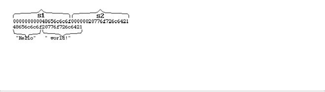
000000000048656c6c6f00000020776f726c6421
Since the string "Hello world!" contains no zero padding, the comparison fails, as shown below:
The above comparison yields a result of zero, which is equivalent to false.
Null string handling
The null string ( "" ) shall be considered equivalent to the ASCII value zero (0), which is different from a string "0" .

3.8 Memories
An array of registers can be used to model read-only memories (ROMs), random access memories (RAMs), and register files. Each register in the array is known as an element or word and is addressed by a single array index. There shall be no arrays with multiple dimensions.
Memories shall be declared in register declaration statements by specifying the element address range after the declared identifier. See 3.2.2. The expressions that specify the indices of the array shall be constant expressions. The value of the constant expression can be a positive integer, a negative integer, or zero.
One declaration statement can be used for declaring both registers and memories This makes it convenient to declare both a memory and some registers that will hold data to be read from and written to the memory in the same declaration statement.
An n-bit register can be assigned a value in a single assignment, but a complete memory cannot. To assign a value to a memory element, an index shall be specified. The index can be an expression. This option provides a mechanism to reference different memory elements, depending on the value of other registers and nets in the circuit. For example, a program counter register could be used to index into a RAM.
Examples:
1. Memory declaration:
reg [7:0] mema[0:255]; // declares a memory mema of 256 eight-bit
//registers. The indices are 0 to 255 parameter
//parameters are run-time constants - see 3.10 wordsize = 16,
memsize = 256;
//Declare 256 words of 16-bit memory plus two regs reg [wordsize-1:0] writereg, // equivalent to [15:0] readreg,
mem [memsize-1:0];// equivalent to [255:0]
2. A memory of n 1-bit registers is different from an n -bit vector register
reg [1:n] rega; // An n-bit register is not the same reg mema [1:n]; // as a memory of n 1-bit registers
3. Assignment to memory elements
rega = 0; // Legal Syntax mema = 0; // Illegal Syntax
mema[1] = 0; // Assigns 0 to the first element of mema
NOTE--Implementations may limit the maximum size of a register array, but will at least be 16777216 (224).
3.9 Integers, reals, times and realtimes
In addition to modeling hardware, there are other uses for registers in an HDL model. Although reg variables can be used for general purposes such as counting the number of times a particular net changes value, the integer and time register data types are provided for convenience and to make the description more self-documenting.
The syntax for declaring integer, time, real and realtime registers is as follows (from Syntax 3-2):
integer_declaration ::= integer list_of_register_identifiers ;
time_declaration ::= time list_of_register_identifiers ;
real_declaration ::= real real_identifier { , real_identifier } ;
realtime_declaration ::= realtime real_identifier { , real_identifier } ;
Syntax 3-3: Syntax for Integer, time, real and realtime declarations
The syntax for list of register variables is defined in section 3.2.2.
An integer is a general purpose register used for manipulating quantities that are not regarded as hardware registers.
A time register is used for storing and manipulating simulation time quantities in situations where timing checks are required and for diagnostics and debugging purposes. This data type is typically used in conjunction with the $time system function (see Section 14).
Arrays of integer and time registers shall be declared in the same manner as arrays of reg type (section 3.8).
The integer and time registers shall be assigned values in the same manner as reg. Procedural assignments shall be used to trigger their value changes.
The time registers shall behave the same as a register of at least 64 bits. They shall be unsigned quantities, and unsigned arithmetic shall be performed on them. In contrast, integer registers shall be treated as signed quantities. Arithmetic operations performed on integer registers shall produce 2's complement results.
The Verilog HDL supports real number constants and real register data type in addition to integer and time register data types. Except for the following restrictions, registers declared as real can be used in the same places that integers and time registers are used:
●Not all Verilog HDL operators can be used with real number values. See Table 4-3 in section 4.1 for lists of valid and invalid operators for real numbers and real registers.
●Real registers shall not use range in the declaration
●Real registers shall default to an initial value of zero.
The realtime declarations shall be treated synonymous with real declarations, and can be used interchangeably.
Examples:
integer a[1:64]; // an array of 64 integer values
time chng_hist[1:1000]; // an array of 1000 time values
real float ; // a register to store real value
realtime rtime ; // a register to store time as a real value
NOTE--Implementations may limit the maximum size of an integer variable, but shall at least be 32 bits.

Operators and real numbers
The result of using logical or relational operators on real numbers and real registers is a single-bit scalar value. Not all Verilog HDL operators can be used with expression involving real numbers and real registers. Table 4-3 in 4.1 lists the valid operators for use with real numbers and real registers. Real number constants and real registers are also prohibited in the following cases:
●edge descriptors (posedge, negedge) applied to real registers
●bit-select or part-select references of variables declared as real
●real number index expressions of bit-select or part-select references of vectors
●declaration of memories (arrays of real registers)
Conversion
Real numbers shall be converted to integers by rounding the real number to the nearest integer, rather than by truncating it. Implicit conversion shall take place when a real number is assigned to an integer. The ties shall be rounded away from zero.
Implicit conversion shall take place when a net or register is assigned to a real. Individual bits that are x or z in the net or the register shall be treated as zero upon conversion.
See Section 14 for a discussion of system tasks that perform explicit conversion.
3.7 Net types
There are several distinct types of nets as shown in Table 3-1.
Table 3-1: Net Types
Wire and tri nets
The wire and tri nets connect elements. The net types wire and tri shall be identical in their syntax and functions; two names are provided so that the name of a net can indicate the purpose of the net in that model. A wire net can be used for nets that are driven by a single gate or continuous assignment. The tri net type can be used where multiple drivers drive a net.
Logical conflicts from multiple sources on a wire or a tri net result in unknown values unless the net is controlled by logic strength.
Table 3-2 is a truth table for wire and tri nets. Note that it assumes equal strengths for both drivers. Please refer to 7.10 for a discussion of logic strength modeling.
Table 3-2: Truth table for wire and tri nets
Wired nets
Wired nets are of type wor , wand , trior , and triand , and are used to model wired logic configurations. Wired nets resolve the conflicts that result when multiple drivers drive the same net. The wor and trior nets shall create wired or configurations, such that when any of the drivers is 1 , the resulting value of the

net is 1 . The wand and triand nets shall create wired and configurations, such that if any driver is 0 , the value of the net is 0 .
The net types wor and trior shall be identical in their syntax and functionality. The net types wand and triand shall be identical in their syntax and functionality. Table 3-3 and Table 3-4 gives the truth tables for wired nets. Note that it assumes equal strengths for both drivers. See 7.10 for a discussion of logic strength modeling.
Table 3-3: Truth tables for wand and triand nets
Table 3-4: Truth tables for wor and trior nets
Trireg net
The trireg net stores a value and is used to model charge storage nodes. A trireg net can be in one of two states:
driven state When at least one driver of a trireg net has a value of 1 , 0 , or x , the resolved value propagates into the trireg net and is the trireg net's driven value.
capacitive state When all the drivers of a trireg net are at the high impedance value ( z ), the trireg net retains its last driven value; the high impedance value does not propagate from the driver to the trireg.
The strength of the value on the trireg net in the capacitive state can be small,

medium, or large, depending on the size specified in the declaration of the trireg net. The strength of a trireg net in the driven state can be supply, strong, pull, or weak depending on the strength of the driver.
Example:
Figure 3-1 shows a schematic that includes a trireg net whose size is medium, its driver, and the simulation results.
Figure 3-1: Simulation values of a trireg and its driver
a)At simulation time 0, wire a and wire b have a value of 1 . A value of 1 with a strong strength propagates from the and gate through the nmos switches connected to each other by wire c , into trireg net d .
b)At simulation time 10, wire a changes value to 0 , disconnecting wire c from the and gate. When wire c is no longer connected to the and gate, value of wire c changes to HiZ . The value of wire b remains 1 so wire c remains connected to trireg net d through the nmos2 switch. The HiZ value does not propagate from wire c into trireg net d . Instead, trireg net d enters the capacitive state, storing its last driven value of 1 . It stores the 1 with a medium strength.
Capacitive networks
A capacitive network is a connection between two or more trireg nets. In a capacitive network whose trireg nets are in the capacitive state, logic and strength values can propagate between trireg nets.
Examples:
Figure 3-2 shows a capacitive network in which the logic value of some trireg nets change the logic value of other trireg nets of equal or smaller size.

Figure 3-2: Simulation results of a capacitive network
In Figure 3-2, capacitive strength of trireg_la net is large , trireg_me1 and trireg_me2 are medium , and trireg_sm is small . Simulation reports the following sequence of events:
a)At simulation time 0, wire a and wire b have a value of 1 . The wire c drives a value of 1 into trireg_la and trireg_sm , wire d drives a value of 1 into trireg_me1 and trireg_me2 .
b)At simulation time 10, value of wire b changes to 0 , disconnecting trireg_sm and trireg_me2 from their drivers. These trireg nets enter the capacitive state and store the value 1 , their last driven value.
c)At simulation time 20, wire c drives a value of 0 into trireg_la .
d)At simulation time 30, wire d drives a value of 0 into trireg_me1 .
e)At simulation time 40, value of wire a changes to 0 , disconnecting trireg_la and trireg_me1 from their drivers. These trireg nets enter

the capacitive state and store the value 0 .
f) At simulation time 50, the value of wire b changes to 1 .
This change of value in wire b connects trireg_sm to trireg_la ; these trireg nets have different sizes and stored different values. This connection causes the smaller trireg net to store the larger trireg net's value and trireg_sm now stores a value of 0 .
This change of value in wire b also connects trireg_me1 to trireg_me2 ; these trireg nets have the same size and stored different values. The connection causes both trireg_me1 and trireg_me2 to change value to x .
In a capacitive network, charge strengths propagate from a larger trireg net to a smaller trireg net. Figure 3-3 shows a capacitive network and its simulation results.
Figure 3-3: Simulation results of charge sharing
In Figure 3-3, capacitive strength of trireg_la is large and capacitive strength of trireg_sm is small. Simulation reports the following results:
a) At simulation time 0, the value of wire a , wire b , and wire c is 1 and wire a drives a strong 1 into trireg_la and trireg_sm .


Supply nets
The supply0 and supply1 nets may be used to model the power supplies in a circuit. These nets shall have supply strengths.
5 Numbers
Constant numbers can be specified as integer constants or real constants.
number ::= decimal_number |
| |
octal_number| binary_number| hex_number| real_number |
decimal_number ::= [ sign |
] |
unsigned_number| [ size ] decimal_base unsigned_number |
binary_number ::= [ size ] binary_base binary_digit { _ | binary_digit }
octal_number ::= [ size ] octal_base octal_digit { _ | octal_digit }
hex_number ::= [ size ] hex_base hex_digit { _ | hex_digit }
real_number ::= |
[ sign ] |
unsigned_number . unsigned_number |
|
|
|
| |
[ sign ] unsigned_number [ . unsigned_number ] e [ sign ] |
unsigned_number |
|
|
|
|
|
| |
[ sign ] unsigned_number [ . unsigned_number ] E [ sign ] |
unsigned_number |
|
|
|
sign ::= + | - |
|
|
|
size ::= unsigned_number |
|
||
unsigned_number ::= |
decimal_digit { _ | decimal_digit } |
||
decimal_base ::= 'd |
| 'D |
|
|
binary_base ::= 'b |
| 'B |
|
|
octal_base ::= 'o |
|
| 'O |
|
hex_base ::= 'h |
| 'H |
|
|
decimal_digit ::= 0 | 1 | |
2 | 3 | 4 | 5 | 6 | 7 | 8 | 9 |
||
binary_digit ::= x | X | z | Z | 0 | 1 |
|||
octal_digit ::= x | X | z |
| Z | 0 | 1 | 2 | 3 | 4 | 5 | 6 | 7 |
||
hex_digit ::= x | X | z | |
Z | 0 | 1 | 2 | 3 | 4 | 5 | 6 | 7 | 8 | 9 | a | b | c | d | |
||
e | f | A | B | C | D | E | F
Syntax 2-1: Syntax for integer and real numbers
Integer constants
Integer constants can be specified in decimal, hexadecimal, octal, or binary format.
There are two forms to express integer constants. The first form is a simple decimal number which shall be specified as a sequence of digits 0 through 9 , optionally starting with a plus or minus unary operator. The second form specifies a sized constant , which shall be composed of up to three tokens - an optional size constant, a single quote followed by a base format character, and the digits representing the value of the number.
The first token, a size constant, shall specify the size of the constant in terms of its exact number of bits. It shall be specified as an unsigned decimal number. For example, the size specification for two hexadecimal digits is 8, because one hexadecimal digit requires four bits.
The second token, a base_format, shall consist of a letter specifying the base for the number, preceded by the single quote character ( ' ). Legal base specifications are d , D , h , H , o , O , b, or B , for the bases decimal, hexadecimal, octal, and binary respectively.
The use of x and z in defining the value of a number is case insensitive.
The single quote and the base format character shall not be separated by any white space.
The third token, an unsigned number, shall consist of digits that are legal for the specified base format. The unsigned number token shall immediately follow the base format, optionally preceded by white space. The hexadecimal digits a to f shall be case insensitive.
Simple decimal numbers without the size and the base format shall be treated as signed integers , whereas the numbers specified with the base format shall be treated as unsigned integers .
A plus or a minus operator preceding the size constant is a sign for the constant number; the size constant does not take a sign. A plus or minus operator between the base format and the number is an illegal syntax.
Negative numbers shall be represented in 2's complement form.
An x represents the unknown value in hexadecimal, octal, and binary constants . A z represents the high impedance value. See section 3.1 for a discussion of the Verilog HDL value set. An x shall set four bits to unknown in the hexadecimal base, three bits in the octal base, and one bit in the binary base. Similarly, a z shall set four, three, and one bit, respectively, to the high impedance value.
If the size of the unsigned number is smaller than the size specified for the constant, the unsigned number shall be padded to the left with zeros. If the left most bit in the unsigned number is an x or a z , then an x or a z shall be used to pad to the left respectively.
When used in a number, the question mark (?) character is a Verilog HDL alternative for the z character. It sets four bits to the high impedance value in hexadecimal numbers, three in octal, and one in binary. The question mark can be used to enhance readability in cases where the high impedance value is a don't-care condition. See the discussion of casez and casexin
section 9.5.1. The question mark character is also used in user defined primitive state table. See section 8.1.4.
The underscore character (_) shall be legal anywhere in a number except as the first or the last character. This feature can be used to break up long numbers for readability purposes.
Examples:
Unsized constant numbers
659 // is a decimal number
'h 837FF // is a hexadecimal number 'o7460 // is an octal number
4af // is illegal (hexadecimal format requires 'h)
Sized constant numbers
4'b1001 // is a 4-bit binary number 5 'D 3 // is a 5-bit decimal number
3'b01x // is a 3-bit number with the least // significant bit unknown
12'hx // is a 12-bit unknown number
16'hz // is a 16-bit high impedance number
Using sign with constant numbers
8 'd -6 // this is illegal syntax
-8 'd 6 // this defines the two's complement of 6, // held in 8 bits--equivalent to -(8'd 6)
Automatic left padding
reg [11:0] a, b, c, d; initial begin
a = 'h x; // yields xxx b = 'h 3x; // yields 03x c = 'h z3; // yields zz3
d = 'h 0z3; // yields 0z3 end
Using underscore character in numbers
27_195_000 16'b0011_0101_0001_1111 32 'h 12ab_f001
NOTES
1)--A sized negative number is not sign-extended when assigned to a register data type.
2)--Each of the three tokens for specifying a number may be macro substituted.
3)--The number of bits that make up an unsized number (which is a simple decimal number or a number without the size specification) shall be at least 32.
Real constants
The real constant numbers shall be represented as described by IEEE STD-754-1985, an IEEE standard for double precision floating point numbers.
Real numbers can be specified in either decimal notation (for example, 14.72) or in scientific notation (for example, 39e8, which indicates 39 multiplied by 10 to the 8th power). Real numbers expressed with a decimal point shall have at least one digit on each side of the decimal point.

Examples:
1.2 0.1 2394.26331 1.2E12 (the exponent symbol can be e or E) 1.30e-2 0.1e-0 23E10 29E-2 236.123_763_e-12 (underscores are ignored)
The following are invalid forms of real numbers because they do not have at least one digit on each side of the decimal point:
.12 9.4.E3 .2e-7
Conversion
Real numbers shall be converted to integers by rounding the real number to the nearest integer, rather than by truncating it. Implicit conversion shall take place when a real number is assigned to an integer. The ties shall be rounded away from zero.
Examples:
The real numbers 35.7 and 35.5 both become 36 when converted to an integer and 35.2 becomes 35.
Converting -1.5 to integer yields -2, converting 1.5 to integer yields 2.
3.10 Parameters
Verilog HDL parameters do not belong to either the register or the net group. Parameters are not variables, they are constants.
The syntax for parameter declarations is as follows:
parameter_declaration ::= parameter list_of_param_assignments ;
list_of_param_assignments ::= param_assignment { , param_assignment }
param_assignment ::= parameter_identifier = constant_expression
Syntax 3-4: Syntax for parameter_declaration
The list of param assignments shall be a comma-separated list of assignments, where the right-hand side of the assignment shall be a constant expression, that is, an expression containing only constant numbers and previously defined parameters.
Parameters represent constants, hence it is illegal to modify their value at runtime. However, parameters can be modified at compilation time to have values that are different from those specified in the declaration assignment. This allows customization of module instances. A parameter can be modified with the defparam statement, or in the module instance statement. Typical uses of parameters are to specify delays and width of variables. See Section 12, for details on parameter value assignment.
Examples:
parameter msb = 7; // defines msb as a constant value 7 parameter e = 25, f = 9; // defines two constant numbers parameter r = 5.7; // declares r as a real parameter parameter byte_size = 8, byte_mask = byte_size - 1; parameter average_delay = (r + f) / 2;

4.1 Operators
The symbols for the Verilog HDL operators are similar to those in the C programming language. Table 4-1 lists these operators.
Table 4-1: Operators in Verilog HDL
Operators with real operands
The operators shown in Table 4-2 shall be legal when applied to real operands. All other operators shall be considered illegal when used with real operands.
Table 4-2: Legal operators for use

in real expressions
The result of using logical or relational operators on real numbers is a single-bit scalar value.
Table 4-3 lists operators that shall not be used to operate on real numbers.
Table 4-3: Operators not allowed for real expressions
See section 3.9.1 for more information on use of real numbers.
Binary operator precedence
The precedence order of binary operators and the conditional operator ( ?: ) is shown below in Table 4-4. Verilog HDL has two equality operators. They are discussed in section 4.1.8.
Table 4-4: Precedence rules for operators

Operators shown on the same row in Table 4-4 shall have the same precedence. Rows are arranged in order of decreasing precedence for the operators. For example, *, /, and % all have the same precedence, which is higher than that of the binary + and - operators.
All operators shall associate left to right with the exception of the conditional operator which shall associate right to left. Associativity refers to the order in which the operators having the same precedence are evaluated. Thus, in the following example B is added to A and then C is subtracted from the result of A+B .
A + B - C
When operators differ in precedence, the operators with higher precedence shall associate first. In the following example, B is divided by C (division has higher precedence than addition) and then the result is added to A .
A + B / C
Parentheses can be used to change the operator precedence.
(A + B) / C // not the same as A + B / C
Using integer numbers in expressions
Integer numbers can be used as operands in expressions. An integer number can be expressed as
●an unsized, unbased integer (e.g. 12)
●an unsized, based integer (e.g. `d12)
●a sized, based integer (e.g. 16'd12)
A negative value for an integer with no base specifier shall be interpreted differently than for an integer with a base specifier. An integer with no base specifier shall be interpreted as a signed value in two's complement form. An integer with a base specifier shall be interpreted as an unsigned value in two's complement form.
This example shows two ways to write the expression "minus 12 divided by 3". Note that -12 and -'d12 both evaluate to the same two's complement bit pattern but in an expression, the -'d12 loses its identity as a signed negative number.
integer IntA;
IntA = -12 / 3; // The result is -4
IntA = -'d 12 / 3; // The result is 1431655761.
Expression evaluation order
The operators shall follow the associativity rules while evaluating an expression as described in section 4.1.2. However, if the final result of an expression can be determined early, the entire expression need not be evaluated. This is called short-circuiting an expression evaluation.
reg regA, regB, regC, result ; result = regA & (regB | regC) ;
If regA is known to be zero, the result of the expression can be determined as zero without evaluating the sub-expression regB | regC .

Arithmetic operators
The binary arithmetic operators are the following:
Table 4-5: Arithmetic
operators defined
The integer division shall truncate any fractional part. The modulus operator, for example y % z , gives the remainder when the first operand is divided by the second, and thus is zero when z divides y exactly. The result of a modulus operation shall take the sign of the first operand.
The unary arithmetic operators shall take precedence over the binary operators. The unary operators are the following:
Table 4-6: Unary operators defined
For the arithmetic operators, if any operand bit value is the unknown value x , or high impedance value z , then the entire result value shall be x .
Table 4-7 gives examples of modulus operations.
Table 4-7: Examples of modulus operations
Arithmetic expressions with registers and integers
An arithmetic operation on a reg type register shall be treated differently than an arithmetic operation on an integer data type. A reg data type shall be treated as an unsigned value and an integer data type shall be treated as a signed value. Thus, if a sized constant with a negative value is stored in a reg type register, a positive constant which is a two's complement of the sized constant shall be the value stored in the reg type register. When this register is used in an arithmetic expression, the positive constant shall be used as the value of the register. In contrast, if a sized constant with a negative value is stored in an integer type register and used in an arithmetic expression, the expression shall evaluate using signed arithmetic.

Table 4-8 lists how arithmetic operators interpret each data type
Table 4-8: Data type interpretation by arithmetic operators
The example below shows various ways to divide "minus twelve by three"--using integer and reg data types in expressions.
integer intA; reg [15:0] regA;
intA = -4'd12; |
|
|
regA = intA / 3; |
// expression |
result is -4, |
|
// intA is an |
integer data type |
regA = -4'd12; |
// regA is 65524 |
|
intA = regA / 3; |
// expression |
result is 21841, |
|
// regA is a reg data type. |
|
intA = -4'd12 / 3; // expression result is 1431655761.
// -4'd12 is effectively a reg data type
regA = -12 / 3; // expression result is -4, -12 is effectively // an integer data type. regA is 65532
Relational operators
Table 4-9 lists and defines the relational operators.
Table 4-9: The relational operators defined
An expression using these relational operators shall yield the scalar value 0 if the specified relation is false , or the value 1 if it is true . If, due to unknown or high impedance bits in the operands, the relation is ambiguous , then the result shall be one bit unknown value (x) .
When two operands of unequal bit-lengths are used, the smaller operand shall be zero filled on the most significant bit side to extend to the size of the larger operand.
All the relational operators shall have the same precedence. Relational operators shall have lower


clearly the precedence intended, as in the following rewrite of the above example:
(a < size-1) && (b != c) && (index != lastone)
3. A common use of ! is in constructions like the following:
if (!inword)
In some cases, the preceding construct makes more sense to someone reading the code than the equivalent construct shown below:
if (inword == 0)
Constructs like if ( ! inword ) read quite nicely (if not inword), but more complicated ones can be hard to understand.
Bit-wise operators
The bit-wise operators shall perform bit-wise manipulations on the operands--that is, the operator shall combine a bit in one operand with its corresponding bit in the other operand to calculate one bit for the result. The logic tables below show the results for each possible calculation.
Table 4-11:
Bit-wise binary and operator
Table 4-12:
Bit-wise binary exclusive or operator
Table 4-13:
Bit-wise binary exclusive or operator

Table 4-14: Bit-wise binary exclusive nor operator
Table 4-15: Bit-wise unary negation operator
When the operands are of unequal bit length, the shorter operand is zero-filled in the most significant bit positions.
Reduction operators
The unary reduction operators shall perform a bit-wise operation on a single operand to produce a single bit result. The first step of the operation shall apply the operator between the first bit of the operand and the second--using the logic tables shown below. The second and subsequent steps shall apply the operator between the one-bit result of the prior step and the next bit of the operand using the same logic table.
Table 4-16: Reduction unary and operator

Table 4-17:
Reduction
unary or
operator
Table 4-18: Reduction unary nand operator
Table 4-19: Reduction unary exclusive nor operator
Table 4-23 shows the results of applying reduction operators on different operands.
Table 4-23: Results of unary reduction operations
Shift operators
The shift operators , << and >>, shall perform left and right shifts of their left operand by the
number of bit positions given by the right operand. Both shift operators shall fill the vacated bit positions with zeroes. If the right operand has an unknown or high impedance value then the result shall be unknown. If the right operand is negative, the result shall remain the same as the left operand--that is, the left operand shall not be shifted.
module shift;
reg [3:0] start, result; initial begin
start = 1;
result = (start << 2);
end endmodule
In this example, the register result is assigned the binary value 0100 , which is 0001 shifted to the left two positions and zero filled.
Conditional operator
The conditional operator , also known as ternary operator , shall be right associative and shall be constructed using three operands separated by two operators in the following format:
conditional_expression ::= expression1 ? expression2 : expression3
Syntax 4-1: Syntax for conditional expression
The evaluation of a conditional expression shall begin with the evaluation of expression1. If expression1 evaluates to false (0), then expression3 shall be evaluated and used as the result of the conditional expression. If expression1 evaluates to true (known value other than 0), then expression2 is evaluated and used as the result. If expression1 evaluates to ambiguous value ( x or z ), then both expression2 and expression3 shall be evaluated and their results shall be combined, bit by bit, using Table 4-24 to calculate the final result. If the lengths of the operands are different, the shorter operand shall be lengthened to match the longer and zero filled from the left (the high-order end).
Table 4-24: Ambiguous condition results for conditional operator
The following example of a tri-state output bus illustrates a common use of the conditional operator.
wire [15:0] busa = drive_busa ? data : 16'bz;
The bus called data is driven onto busa when drive_busa is 1 . If drive_busa is unknown, then an unknown value is driven onto busa . Otherwise, busa is not driven.
Concatenations
A concatenation is the joining together of bits resulting from two or more expressions. The

concatenation shall be expressed using the brace characters { and }, with commas separating the expressions within.
Unsized constant numbers shall not be allowed in concatenations. This is because the size of each operand in the concatenation is needed to calculate the complete size of the concatenation.
The next example concatenates four expressions:
{a, b[3:0], w, 3'b101}
and it is equivalent to the following example:
{a, b[3], b[2], b[1], b[0], w, 1'b1, 1'b0, 1'b1}
Concatenations can be expressed using a repetition multiplier as shown in the next example.
{4{w}} // This is equivalent to {w, w, w, w}
If a repetition multiplier is used on a function call operand, the function need not be evaluated multiple times. For example,
result = {4{func(w)}}
may be computed as
result = {func(w), func(w), func(w), func(w)}
or
y = func(w) ;result = {y, y, y, y}
This is another form of expression evaluation short-circuiting.
The next example illustrates nested concatenations.
{b, {3{a, b}}} // This is equivalent to {b, a, b, a, b, a, b}
The repetition multiplier must be a constant expression.
2.6 Strings
A string is a sequence of characters enclosed by double quotes ( "" ) and contained on a single line. Strings used as operands in expressions and assignments shall be treated as unsigned integer constants represented by a sequence of eight-bit ASCII values, with one eight bit ASCII value representing one character.
String variable declaration
String variables are variables of register type (see section 3.2) with width equal to the number of characters in the string multiplied by 8.
Example:
To store the twelve characters string "Hello world!" requires a register 8*12, or 96 bits wide
reg [8*12:1] stringvar; initial begin
stringvar = "Hello world!"; end
String manipulation
Strings can be manipulated using the Verilog HDL operators. The value being manipulated by the operator is the sequence of 8-bit ASCII values.
Example:
module string_test;
reg [8*14:1] stringvar; initial
begin stringvar = "Hello world";
$display("%s is stored as %h", stringvar,stringvar); stringvar = {stringvar,"!!!"};
$display("%s is stored as %h", stringvar,stringvar);
end endmodule
The output is:
Hello world is stored as 00000048656c6c6f20776f726c64 Hello world!!! is stored as 48656c6c6f20776f726c64212121
NOTE--When a variable is larger than required to hold a value being assigned, the contents on the left are padded with zeros after the assignment. This is consistent with the padding that occurs during assignment of non-string values. If a string is larger than the destination string variable, the string is truncated to the left and the left most characters will be lost.

Special characters in strings
Certain characters can only be used in strings when preceded by an introductory character called an escape character. Table 2-1 lists these characters in the right-hand column with the escape sequence that represents the character in the left-hand column.
Table 2-1: Specifying special characters in string

4.3 Minimum, typical, maximum delay expressions
Verilog HDL delay expressions can be specified as three expressions separated by colons. This triple is intended to represent minimum, typical, and maximum values--in that order. The syntax is as follows:
mintypmax_expression ::= expression
| expression : expression : expression
Syntax 4-2: Syntax for mintypmax expression
Verilog HDL models typically specify three values for delay expressions. The three values allow a design to be tested with minimum, typical, or maximum delay values.
Values expressed in min:typ:max format can be used in expressions. The min:typ:max format can be used wherever expressions can appear.
1. This example shows an expression that defines a single triplet of delay values. The minimum value is the sum of a+d ; the typical value is b+e ; the maximum value is c+f , as follows:
(a:b:c) + (d:e:f)
3. The next example shows some typical expressions that are used to specify min:typ:max format values:
val - (32'd 50: 32'd 75: 32'd 100)
Last Edited by SP 14112004
LOGIC
SYNTHESIS
Logic synthesis provides a link between an HDL (Verilog or VHDL) and a netlist similarly to the way that a C compiler provides a link between C code and machine language. However, the parallel is not exact. C was developed for use with compilers, but HDLs were not developed for use with logic-synthesis tools. Verilog was designed as a simulation language and VHDL was designed as a documentation and description language. Both Verilog and VHDL were developed in the early 1980s, well before the introduction of commercial logic-synthesis software. Because these HDLs are now being used for purposes for which they were not intended, the state of the art in logic synthesis falls far short of that for computer-language compilers. Logic synthesis forces designers to use a subset of both Verilog and VHDL. This makes using logic synthesis more difficult rather than less difficult. The current state of synthesis software is rather like learning a foreign language, and then having to talk to a five-year-old. When talking to a logic-synthesis tool using an HDL, it is necessary to think like hardware, anticipating the netlist that logic synthesis will produce. This situation should improve in the next five years, as logic synthesizers mature.
Designers use graphic or text design entry to create an HDL behavioral model , which does not contain any references to logic cells. State diagrams, graphical datapath descriptions, truth tables, RAM/ROM templates, and gate-level schematics may be used together with an HDL description. Once a behavioral HDL model is complete, two items are required to proceed: a logic synthesizer (software and documentation) and a cell library (the logic cells NAND gates and such) that is called the target library . Most synthesis software companies produce only software. Most ASIC vendors produce only cell libraries. The behavioral model is simulated to check that the design meets the specifications and then the logic synthesizer is used to generate a netlist, a structural model , which contains only references to logic cells. There is no standard format for the netlists that logic synthesis produces, but EDIF is widely used. Some logic-synthesis tools can also create structural HDL (Verilog, VHDL, or both). Following logic synthesis the design is simulated again, and the results are compared with the earlier behavioral simulation. Layout for any type of ASIC may be generated from the structural model produced by logic synthesis.
12.1 A Logic-Synthesis
Example
As an example of logic synthesis, we will compare two implementations of the Viterbi decoder described in Chapter 11. Both versions used logic cells from a VLSI Technology cell library. The first ASIC was designed by hand using schematic entry and a data book. The second version of the ASIC (the one that was fabricated) used Verilog for design entry and a logic synthesizer. Table 12.1 compares the two versions. The synthesized ASIC is 16 percent smaller and 13 percent faster than the hand-designed version.
How does logic synthesis generate smaller and faster circuits? Figure 12.1 shows the schematic for a hand-designed comparator and MUX used in the Viterbi decoder ASIC, called here the comparator/MUX example. The Verilog code and the schematic in Figure 12.1 describe the same function. The comparison, in Table 12.2 , of the two design approaches shows that the synthesized version is smaller and faster than the hand design, even though the synthesized design uses more cells.
TABLE 12.1 A comparison of hand design with synthesis (using a 1.0 m m VLSI Technology cell library).
|
Path |
No. of |
|
Chip area/ |
|
delay/ |
No. of transistors |
||
|
standard cells |
mils 2 ( 2 ) |
||
|
ns ( 1 ) |
|||
|
|
|
|
|
Hand design |
41.6 |
1,359 |
16,545 |
21,877 |
Synthesized design |
36.3 |
1,493 |
11,946 |
18,322 |

|
|
|
// comp_mux.v |
|
|
|
|
module comp_mux(a, |
|
|
|
|
b, outp); |
|
|
|
|
input [2:0] a, b; |
|
|
|
|
output [2:0] outp; |
|
|
|
|
function [2:0] |
|
|
|
|
compare; |
|
|
|
|
input [2:0] ina, inb; |
|
|
|
|
begin |
|
|
|
|
if (ina <= inb) |
|
|
|
|
compare = ina; |
|
|
|
|
else compare = inb; |
|
|
|
|
end |
|
|
|
|
endfunction |
|
|
|
|
assign outp = |
|
|
|
|
compare(a, b); |
|
|
|
|
endmodule |
|
FIGURE 12.1 Schematic and HDL design entry. |
|
|
||
TABLE 12.2 Comparison of the comparator/MUX designs using a 1.0 m m |
||||
standard-cell library. |
|
|
|
|
|
Delay /ns |
No. of standard cells |
No. of |
Area |
|
transistors |
/mils 2 |
||
|
|
|
||
Hand design |
4.3 |
12 |
116 |
68.68 |
Synthesized |
2.9 |
15 |
66 |
46.43 |
1.These delays are under nominal operating conditions with no wiring capacitance. This is the only stage at which a comparison could be made because the hand design was not completed.
2.Both figures are initial layout estimates using default power-bus and signal routing widths.