

3.3 Logical Effort
In this section we explore a delay model based on logical effort, a term coined by Ivan Sutherland and Robert Sproull [1991], that has as its basis the time-constant analysis of Carver Mead, Chuck Seitz, and others.
We add a catch all nonideal component of delay, tq , to Eq. 3.2 that includes:
(1) delay due to internal parasitic capacitance; (2) the time for the input to reach the switching threshold of the cell; and (3) the dependence of the delay on the slew rate of the input waveform. With these assumptions we can express the delay as follows:
t PD = R ( C out + C p ) + t q . (3.10)
(The input capacitance of the logic cell is C , but we do not need it yet.)
We will use a standard-cell library for a 3.3 V, 0.5 m m (0.6 m m drawn) technology (from Compass) to illustrate our model. We call this technology C5 ; it is almost identical to the G5 process from Section 2.1 (the Compass library uses a more accurate and more complicated SPICE model than the generic process). The equation for the delay of a 1X drive, two-input NAND cell is in the form of Eq. 3.10 ( C out is in pF):
t PD = (0.07 + 1.46 C out + 0.15) ns . (3.11)
The delay due to the intrinsic output capacitance (0.07 ns, equal to RC p ) and the nonideal delay ( t q = 0.15 ns) are specified separately. The nonideal delay is a considerable fraction of the total delay, so we may hardly ignore it. If data books do not specify these components of delay separately, we have to estimate the fractions of the constant part of a delay equation to assign to RC p and t q (here the ratio RC p / t q is approximately 2).
The data book tells us the input trip point is 0.5 and the output trip points are 0.35 and 0.65. We can use Eq. 3.11 to estimate the pull resistance for this cell as R ª
1.46 nspF 1 or about 1.5 k W . Equation 3.11 is for the falling delay; the data
book equation for the rising delay gives slightly different values (but within 10 percent of the falling delay values).
We can scale any logic cell by a scaling factor s (transistor gates become s times wider, but the gate lengths stay the same), and as a result the pull resistance R will decrease to R / s and the parasitic capacitance C p will increase to sC p .
Since t q is nonideal, by definition it is hard to predict how it will scale. We shall assume that t q scales linearly with s for all cells. The total cell delay then scales as follows:
t PD = ( R / s )·( C out + sC p ) + st q . (3.12)
For example, the delay equation for a 2X drive ( s = 2), two-input NAND cell is
t PD = (0.03 + 0.75 C out + 0.51) ns . (3.13)
Compared to the 1X version (Eq. 3.11 ), the output parasitic delay has decreased
to 0.03 ns (from 0.07 ns), whereas we predicted it would remain constant (the difference is because of the layout); the pull resistance has decreased by a factor of 2 from 1.5 k W to 0.75 k W , as we would expect; and the nonideal delay has increased to 0.51 ns (from 0.15 ns). The differences between our predictions and the actual values give us a measure of the model accuracy.
We rewrite Eq. 3.12 using the input capacitance of the scaled logic cell, C in = s C ,
C out
t PD = RC + RC p + st q . (3.14)
C in
Finally we normalize the delay using the time constant formed from the pull resistance R inv and the input capacitance C inv of a minimum-size inverter:
( RC ) ( C out / C in ) + RC p + st q
d = |
= f + p + q . (3.15) |
t |
|
The time constant tau , |
|
t = R inv C inv , (3.16) |
|
is a basic property of any CMOS technology. We shall measure delays in terms of t .
The delay equation for a 1X (minimum-size) inverter in the C5 library is
t PDf = R pd ( C out + C p ) ln (1/0.35) ª R pd ( C out + C p ) . (3.17)
Thus tq inv = 0.1 ns and R inv = 1.60 k W . The input capacitance of the 1X inverter (the standard load for this library) is specified in the data book as C inv =
0.036 pF; thus t = (0.036 pF)(1.60 k W ) = 0.06 ns for the C5 technology.
The use of logical effort consists of rearranging and understanding the meaning of the various terms in Eq. 3.15 . The delay equation is the sum of three terms,
d = f + p + q . (3.18)
We give these terms special names as follows:
delay = effort delay + parasitic delay + nonideal delay . (3.19)
The effort delay f we write as a product of logical effort, g , and electrical effort, h:
f = gh . (3.20)
So we can further partition delay into the following terms:
delay = logical effort ¥ electrical effort + parasitic delay + nonideal delay . (3.21)
The logical effort g is a function of the type of logic cell,
g = RC/ t . (3.22)
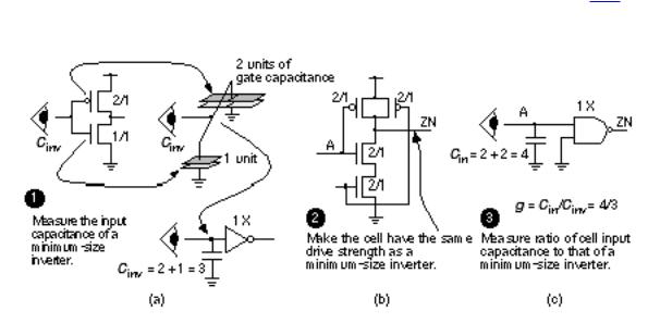
What size of logic cell do the R and C refer to? It does not matter because the R and C will change as we scale a logic cell, but the RC product stays the same the logical effort is independent of the size of a logic cell. We can find the logical effort by scaling down the logic cell so that it has the same drive capability as the 1X minimum-size inverter. Then the logical effort, g , is the ratio of the input capacitance, C in , of the 1X version of the logic cell to C inv (see Figure 3.8 ).
FIGURE 3.8 Logical effort. (a) The input capacitance, C inv , looking into the input of a minimum-size inverter in terms of the gate capacitance of a minimum-size device. (b) Sizing a logic cell to have the same drive strength as a minimum-size inverter (assuming a logic ratio of 2). The input capacitance looking into one of the logic-cell terminals is then C in . (c) The logical effort of a cell is C in / C inv . For a two-input NAND cell, the logical effort, g = 4/3.
The electrical effort h depends only on the load capacitance C out connected to the output of the logic cell and the input capacitance of the logic cell, C in ; thus

h = C out / C in . (3.23)
The parasitic delay p depends on the intrinsic parasitic capacitance C p of the logic cell, so that
p = RC p / t . (3.24)
Table 3.2 shows the logical efforts for single-stage logic cells. Suppose the
minimum-size inverter has an n -channel transistor with W/L = 1 and a p -channel transistor with W/L = 2 (logic ratio, r , of 2). Then each two-input NAND logic cell input is connected to an n -channel transistor with W/L = 2 and a p -channel transistor with W/L = 2. The input capacitance of the two-input NAND logic cell divided by that of the inverter is thus 4/3. This is the logical effort of a two-input NAND when r = 2. Logical effort depends on the ratio of the logic. For an n -input NAND cell with ratio r , the p -channel transistors are W/L = r /1, and the n -channel transistors are W/L = n /1. For a NOR cell the n -channel transistors are 1/1 and the p -channel transistors are nr /1.
TABLE 3.2 Cell effort, parasitic delay, and nonideal delay (in units of t ) for single-stage CMOS cells.
Cell |
Cell effort |
Cell effort |
|
|
Nonideal delay/ |
|
(logic ratio = 2) |
(logic ratio = r) |
Parasitic delay/ t t |
||||
|
|
|
|
|||
|
|
|
p inv (by |
q inv (by |
||
inverter |
1 (by definition) 1 (by definition) definition) 1 |
definition) 1 |
||||
n -input |
( n + 2)/3 |
( n + r )/( r + 1) |
n p inv |
|
n q inv |
|
NAND |
||||||
|
|
|
|
|
||
n -input |
(2 n + 1)/3 |
( nr + 1)/( r + 1) |
n p inv |
n q inv |
||
NOR |
||||||
|
|
|
|
|
||
The parasitic delay arises from parasitic capacitance at the output node of a single-stage logic cell and most (but not all) of this is due to the source and drain capacitance. The parasitic delay of a minimum-size inverter is
p inv = C p / C inv . (3.25)
The parasitic delay is a constant, for any technology. For our C5 technology we know RC p = 0.06 ns and, using Eq. 3.17 for a minimum-size inverter, we can calculate p inv = RC p / t = 0.06/0.06 = 1 (this is purely a coincidence). Thus C p is about equal to C inv and is approximately 0.036 pF. There is a large error in calculating p inv from extracted delay values that are so small. Often we can calculate p inv more accurately from estimating the parasitic capacitance from layout.
Because RC p is constant, the parasitic delay is equal to the ratio of parasitic capacitance of a logic cell to the parasitic capacitance of a minimum-size
inverter. In practice this ratio is very difficult to calculate it depends on the layout. We can approximate the parasitic delay by assuming it is proportional to the sum of the widths of the n -channel and p -channel transistors connected to the output. Table 3.2 shows the parasitic delay for different cells in terms of p inv
.
The nonideal delay q is hard to predict and depends mainly on the physical size of the logic cell (proportional to the cell area in general, or width in the case of a standard cell or a gate-array macro),
q = st q / t . (3.26)
We define q inv in the same way we defined p inv . An n -input cell is approximately n times larger than an inverter, giving the values for nonideal delay shown in Table 3.2 . For our C5 technology, from Eq. 3.17 , q inv = t q inv / t = 0.1 ns/0.06 ns = 1.7.
3.3.1 Predicting Delay
As an example, let us predict the delay of a three-input NOR logic cell with 2X drive, driving a net with a fanout of four, with a total load capacitance (comprising the input capacitance of the four cells we are driving plus the interconnect) of 0.3 pF.
From Table 3.2 we see p = 3 p inv and q = 3 q inv for this cell. We can calculate C in from the fact that the input gate capacitance of a 1X drive, three-input NOR
logic cell is equal to gC inv , and for a 2X logic cell, C in = 2 gC inv . Thus,
C out g ·(0.3 pF) (0.3 pF)
gh = g = = . (3.27)
C in 2 g C inv |
(2)·(0.036 pF) |
(Notice that g cancels out in this equation, we shall discuss this in the next section.)
The delay of the NOR logic cell, in units of t , is thus
0.3 ¥ 10 12
d = gh + p + q = + (3)·(1) + (3)·(1.7) (2)·(0.036 ¥ 10 12 )
= 4.1666667 + 3 + 5.1 |
|
= 12.266667 t . |
(3.28) |
equivalent to an absolute delay, t PD ª 12.3 ¥ 0.06 ns = 0.74 ns.
The delay for a 2X drive, three-input NOR logic cell in the C5 library is
t PD = (0.03 + 0.72 C out + 0.60) ns . (3.29)
With C out = 0.3 pF,
t PD = 0.03 + (0.72)·(0.3) + 0.60 = 0.846 ns . (3.30)
compared to our prediction of 0.74 ns. Almost all of the error here comes from the inaccuracy in predicting the nonideal delay. Logical effort gives us a method to examine relative delays and not accurately calculate absolute delays. More important is that logical effort gives us an insight into why logic has the delay it does.
3.3.2 Logical Area and Logical Efficiency
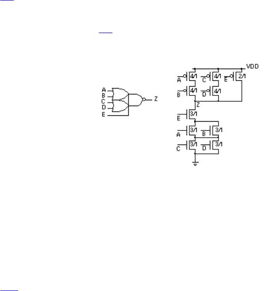
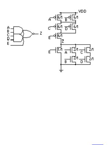
Figure 3.9 shows a single-stage OR-AND-INVERT cell that has different logical
efforts at each input. The logical effort for the OAI221 is the logical-effort vector g = (7/3, 7/3, 5/3). For example, the first element of this vector, 7/3, is the logical effort of inputs A and B in Figure 3.9 .
FIGURE 3.9 An OAI221 logic cell with different logical efforts at each input. In this case g = (7/3, 7/3, 5/3). The logical effort for inputs A and B is 7/3, the logical effort for inputs C and D is also 7/3, and for input E the logical effort is 5/3. The logical area is the sum of the transistor areas, 33 logical squares.
We can calculate the area of the transistors in a logic cell (ignoring the routing area, drain area, and source area) in units of a minimum-size n -channel transistorwe call these units logical squares . We call the transistor area the logical area . For example, the logical area of a 1X drive cell, OAI221X1, is calculated as follows:
●n -channel transistor sizes: 3/1 + 4 ¥ (3/1)
●p -channel transistor sizes: 2/1 + 4 ¥ (4/1)
●total logical area = 2 + (4 ¥ 4) + (5 ¥ 3) = 33 logical squares
Figure 3.10 shows a single-stage AOI221 cell, with g = (8/3, 8/3, 6/3). The calculation of the logical area (for a AOI221X1) is as follows:
● n -channel transistor sizes: 1/1 + 4 ¥ (2/1)
●p -channel transistor sizes: 6/1 + 4 ¥ (6/1)
●logical area = 1 + (4 ¥ 2) + (5 ¥ 6) = 39 logical squares
FIGURE 3.10 An AND-OR-INVERT cell, an AOI221, with logical-effort vector, g = (8/3, 8/3, 7/3). The logical area is 39 logical squares.
These calculations show us that the single-stage AOI221, with an area of 33 logical squares and logical effort of (7/3, 7/3, 5/3), is more logically efficient than the single-stage OAI221 logic cell with a larger area of 39 logical squares and larger logical effort of (8/3, 8/3, 6/3).
3.3.3 Logical Paths
When we calculated the delay of the NOR logic cell in Section 3.3.1, the answer did not depend on the logical effort of the cell, g (it cancelled out in Eqs. 3.27
and 3.28 ). This is because g is a measure of the input capacitance of a 1X drive logic cell. Since we were not driving the NOR logic cell with another logic cell, the input capacitance of the NOR logic cell had no effect on the delay. This is what we do in a data book we measure logic-cell delay using an ideal input waveform that is the same no matter what the input capacitance of the cell. Instead let us calculate the delay of a logic cell when it is driven by a minimum-size inverter. To do this we need to extend the notion of logical effort.
So far we have only considered a single-stage logic cell, but we can extend the idea of logical effort to a chain of logic cells or logical path . Consider the logic path when we use a minimum-size inverter ( g 0 = 1, p 0 = 1, q 0 = 1.7) to drive one input of a 2X drive, three-input NOR logic cell with g 1 = ( nr + 1)/( r + 1), p 1 = 3, q 1 =3, and a load equal to four standard loads. If the logic ratio is r = 1.5, then g 1 = 5.5/2.5 = 2.2.
The delay of the inverter is
d = g 0 h 0 + p 0 + q 0 = (1) · (2g 1 ) · (C inv /C inv ) +1 + 1.7 (3.31)
=(1)(2)(2.2) + 1 + 1.7
=7.1 .
Of this 7.1 t delay we can attribute 4.4 t to the loading of the NOR logic cell input capacitance, which is 2 g 1 C inv . The delay of the NOR logic cell is, as before, d 1 = g 1 h 1 + p 1 + q 1 = 12.3, making the total delay 7.1 + 12.3 = 19.4, so the absolute delay is (19.4)(0.06 ns) = 1.164 ns, or about 1.2 ns.
We can see that the path delay D is the sum of the logical effort, parasitic delay, and nonideal delay at each stage. In general, we can write the path delay as
D = |
g i h i + |
( p i + q i ) . (3.32) |
i path |
i path |
|
3.3.4 Multistage Cells
Consider the following function (a multistage AOI221 logic cell):
ZN(A1, A2, B1, B2, C)
=NOT(NAND(NAND(A1, A2), AOI21(B1, B2, C)))
=(((A1·A2)' · (B1·B2 + C)')')'
=(A1·A2 + B1·B2 + C)'
= AOI221(A1, A2, B1, B2, C) . |
(3.33) |
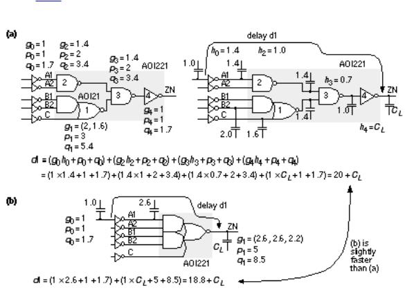
Figure 3.11 (a) shows this implementation with each input driven by a
minimum-size inverter so we can measure the effect of the cell input capacitance.
FIGURE 3.11 Logical paths. (a) An AOI221 logic cell constructed as a multistage cell from smaller cells. (b) A single-stage AOI221 logic cell.
The logical efforts of each of the logic cells in Figure 3.11 (a) are as follows:
g 0 = g 4 = g (NOT) = 1 ,
g 1 = g (AOI21) = (2, (2 r + 1)/( r + 1)) = (2, 4/2.5) = (2, 1.6) ,
g 2 = g 3 = g (NAND2) = ( r + 2)/( r + 1) = (3.5)/(2.5) = 1.4 . (3.34)
Each of the logic cells in Figure 3.11 has a 1X drive strength. This means that
the input capacitance of each logic cell is given, as shown in the figure, by gC inv
.
Using Eq. 3.32 we can calculate the delay from the input of the inverter driving
A1 to the output ZN as
d 1 = (1)·(1.4) + 1 + 1.7 + (1.4)·(1) + 2 + 3.4
+ (1.4)·(0.7) + 2 + 3.4 + (1)· C L + 1 + 1.7
= (20 + C L ) . |
(3.35) |
In Eq. 3.35 we have normalized the output load, C L , by dividing it by a standard load (equal to C inv ). We can calculate the delays of the other paths similarly.
More interesting is to compare the multistage implementation with the single-stage version. In our C5 technology, with a logic ratio, r = 1.5, we can calculate the logical effort for a single-stage AOI221 logic cell as
g (AOI221) = ((3 r + 2)/( r + 1), (3 r + 2)/( r + 1), (3 r + 1)/( r + 1))
= (6.5/2.5, 6.5/2.5, 5.5/2.5) |
|
= (2.6, 2.6, 2.2) . |
(3.36) |
This gives the delay from an inverter driving the A input to the output ZN of the single-stage logic cell as
d1 = ((1)·(2.6) + 1 + 1.7 + (1)· C L + 5 + 8.5 )
= 18.8 + C L . |
(3.37) |
The single-stage delay is very close to the delay for the multistage version of this logic cell. In some ASIC libraries the AOI221 is implemented as a multistage logic cell instead of using a single stage. It raises the question: Can we make the multistage logic cell any faster by adjusting the scale of the intermediate logic cells?
3.3.5 Optimum Delay
Before we can attack the question of how to optimize delay in a logic path, we shall need some more definitions. The path logical effort G is the product of logical efforts on a path:

G = |
g i . (3.38) |
i path |
|
The path electrical effort H is the product of the electrical efforts on the path, |
|
|
C out |
H = |
h i , (3.39) |
i path |
C in |
where C out is the last output capacitance on the path (the load) and C in is the first input capacitance on the path.
The path effort F is the product of the path electrical effort and logical efforts,
F = GH . (3.40)
The optimum effort delay for each stage is found by minimizing the path delay D by varying the electrical efforts of each stage h i , while keeping H , the path electrical effort fixed. The optimum effort delay is achieved when each stage operates with equal effort,
f^ i = g i h i = F 1/ N . (3.41)
This a useful result. The optimum path delay is then
D^ = NF 1/ N = N ( GH ) 1/ N + P + Q , (3.42)
where P + Q is the sum of path parasitic delay and nonideal delay,
P + Q = |
p i + h i . (3.43) |
i path |
|
We can use these results to improve the AOI221 multistage implementation of Figure 3.11 (a). Assume that we need a 1X cell, so the output inverter (cell 4) must have 1X drive strength. This fixes the capacitance we must drive as C out = C inv (the capacitance at the input of this inverter). The input inverters are included to measure the effect of the cell input capacitance, so we cannot cheat by altering these. This fixes the input capacitance as C in = C inv . In this case H = 1.
The logic cells that we can scale on the path from the A input to the output are NAND logic cells labeled as 2 and 3. In this case
G = g 0 ¥ g 2 ¥ g 3 = 1 ¥ 1.4 ¥ 1.4 = 1.95 . (3.44)
Thus F = GH = 1.95 and the optimum stage effort is 1.95 (1/3) = 1.25, so that the optimum delay NF 1/ N = 3.75. From Figure 3.11 (a) we see that

g 0 h 0 + g 2 h 2 + g 3 h 3 = 1.4 + 1.3 + 1 = 3.8 . (3.45)
This means that even if we scale the sizes of the cells to their optimum values, we only save a fraction of a t (3.8 3.75 = 0.05). This is a useful result (and one that is true in general) the delay is not very sensitive to the scale of the cells. In this case it means that we can reduce the size of the two NAND cells in the multicell implementation of an AOI221 without sacrificing speed. We can use logical effort to predict what the change in delay will be for any given cell sizes.
We can use logical effort in the design of logic cells and in the design of logic that uses logic cells. If we do have the flexibility to continuously size each logic cell (which in ASIC design we normally do not, we usually have to choose from 1X, 2X, 4X drive strengths), each logic stage can be sized using the equation for the individual stage electrical efforts,
F 1/ N
h^ i = . (3.46) g i
For example, even though we know that it will not improve the delay by much, let us size the cells in Figure 3.11 (a). We shall work backward starting at the
fixed load capacitance at the input of the last inverter.
For NAND cell 3, gh = 1.25; thus (since g = 1.4), h = C out / C in = 0.893. The output capacitance, C out , for this NAND cell is the input capacitance of the
inverter fixed as 1 standard load, C inv . This fixes the input capacitance, C in , of NAND cell 3 at 1/0.893 = 1.12 standard loads. Thus, the scale of NAND cell 3 is 1.12/1.4 or 0.8X.
Now for NAND cell 2, gh = 1.25; C out for NAND cell 2 is the C in of NAND cell 3. Thus C in for NAND cell 2 is 1.12/0.893 = 1.254 standard loads. This
means the scale of NAND cell 2 is 1.254/1.4 or 0.9X.
The optimum sizes of the NAND cells are not very different from 1X in this case because H = 1 and we are only driving a load no bigger than the input capacitance. This raises the question: What is the optimum stage effort if we have to drive a large load, H >> 1? Notice that, so far, we have only calculated the optimum stage effort when we have a fixed number of stages, N . We have said nothing about the situation in which we are free to choose, N , the number of stages.
3.3.6 Optimum Number of Stages
Suppose we have a chain of N inverters each with equal stage effort, f = gh . Neglecting parasitic and nonideal delay, the total path delay is Nf = Ngh = Nh , since g = 1 for an inverter. Suppose we need to drive a path electrical effort H ;
then h N = H , or N ln h = ln H . Thus the delay, Nh = h ln H /ln h . Since ln H is fixed, we can only vary h /ln ( h ). Figure 3.12 shows that this is a very shallow
function with a minimum at h = e ª 2.718. At this point ln h = 1 and the total delay is N e = e ln H . This result is particularly useful in driving large loads either on-chip (the clock, for example) or off-chip (I/O pad drivers, for example).
FIGURE 3.12 Stage effort.
h |
h/(ln h) |
1.53.7
2 2.9
2.72.7
32.7
42.9
53.1
104.3
Figure 3.12 shows us how to minimize delay regardless of area or power and
neglecting parasitic and nonideal delays. More complicated equations can be derived, including nonideal effects, when we wish to trade off delay for smaller area or reduced power.
1. For the Compass 0.5 m m technology (C5): p inv = 1.0, q inv = 1.7, R inv = 1.5 k W , C inv = 0.036 pF.