


3.9 Summary
In this chapter we covered ASIC libraries: cell design, layout, and characterization. The most important concepts that we covered in this chapter were
●Tau, logical effort, and the prediction of delay
●Sizes of cells, and their drive strengths
●Cell importance
●The difference between gate-array macros, standard cells, and datapath cells

3.10 Problems
* = difficult, ** = very difficult, *** = extremely difficult
3.1(Pull resistance, 10 min.)
●a. Show that, for small V DS , an n -channel transistor looks like a resistor, R = 1/( b n ( V DD Vt n )).
●b. If V GS = V DD , V DS = 0, and k ' n = 200 m AV 2 (equal to the n -channel transistor SPICE parameter KP in Table 2.1), find the pull resistance, R , for a 6/0.6 transistor in the linear region.
Answer: (b) 213 W .
3.2 (Inversion layer depth, 15 min.) In the absence of surface charge, Gauss s law demands continuity of the electric displacement vector, D = e E , at the silicon surface, so that e ox E ox = e Si E Si , where e ox = 3.9, e Si = 11.7.
●a. Assuming the potential at the surface is V GS Vt = 2.5 V, calculate E ox and E Si if T ox = 100 Å.
●b. Assume that carrier density exp ( q f /kT), where f is the potential; calculate the distance below the surface at which the inversion charge density falls to 10 percent of its value at the surface.
●c. Comment on the accuracy of your answers.
Answer: (a) 2.5 ¥ 10 8 Vm 1 , 0.833 ¥ 10 8 Vm 1 . (b) 7.16 Å.
3.3 (Depletion layer depth, 15 min.) The depth of the depletion region under the gate is given by x d = ÷[ (2 e Si f s )/(qN A )], where f s = 2V T ln(N A /n i ) is the surface potential at strong inversion. Calculate f s and x d assuming: e Si =1.0359 ¥ 10 10 Fm 1
, the substrate doping, N A = 1.4 ¥ 10 17 cm 3 , the intrinsic carrier concentration n i = 1.45 ¥ 10 10 cm 3 (at room temperature), and the thermal voltage V T = kT/q = 25.9 mV.
Answer: 0.833 V, 900 Å.
3.4(Logical effort, 45 min.) Calculate the logical effort at each input of an AOI122 cell. Find an expression that allows you to calculate the logical effort for each input of an AOI nnnn cell for n = 1, 2, 3.
3.5(Gate-array macro design, 120 min.) Draw a 1X drive, two-input NAND cell using the gate-array base cells shown in Figures 3.14 (a) 3.16 (lay a piece of thin paper over
the figures and draw the contacts and metal personalization only). Label the inputs and outputs. Lay out a 1X drive, four-input NAND cell using the same base array cells.
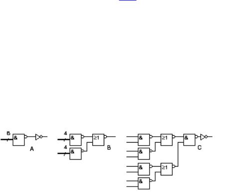
Now lay out a 2X drive, four-input NAND cell (think about this one). Make sure that you size your transistors properly to balance rise times and fall times.
3.6(Flip-flop library, 20 min.) Suppose we wish to build a library of flip-flops. We want to have flops with: positive-edge and negative-edge triggering: clear, preset (either, both, or neither); synchronous or asynchronous reset and preset controls if present (but not mixed on the same flip-flop); all flip-flops with or without scan as an option; flip-flops with Q and Qbar (either or both). How many flip-flops is that? (***) How would you attempt to prioritize which flip-flops to include in a library?
3.7(AOI and OAI cell ratios, 30 min.) In Figure 2.13(c) we adjusted the sizes of the transistors assuming that there was only one path through the n -channel and p -channel stacks. Suppose that p -channel transistors A, B, C, and D are all on and p -channel transistor E turns on. What is the equivalent resistance of the p -channel stack in this case?
3.8(**Eight-input AND, 60 min.) This question is an example in the paper by Sutherland and Sproull [1991] on logical effort. Figure 3.24 shows three different
ways to design an eight-input AND cell, using NAND and NOR cells.
●a. Find the logical effort at each input for A, B, C. Assume a logic ratio of 2.
●b. Find the parasitic delay for A, B, C. Assume the parasitic delay of an inverter is 0.6.
●c. Show that the path delays are given by the following equations where H is the path electrical effort, if we ignore the nonideal delays:
●(i) 2 (3.33 H ) 0.5 + 5.4 (alternative A)
●(ii) 2 (3.33 H ) 0.5 + 3.6 (alternative B)
●(iii) 4 (2.96 H ) 0.25 + 4.2 (alternative C)
●d. Use these equations to determine the best alternative for H = 2 and H = 32.
FIGURE 3.24 An eight-input AND cell (Problem 3.8 ).
3.9 (Special logic cells, 30 min.) Many ASIC cell libraries contain special logic cells. For example the Compass libraries contain a two-input NAND cell with an inverted input, FN01 = (A + B'). This saves routing area, is faster than using two separate cells, and is useful because the combination of a two-input NAND gate with one inverted input is heavily used by synthesis tools. Other special cells include:
●FN02 = MAJ3 = (A·B + A·C + B·C)'
●FN03 = AOI2-2 = ((A'·B') + (C·D))' = (A + B)(C' + D') = OA2-2
●FN04 = OAI2-2
●FN05 = A·B' = (A' + B)'
●a. Draw schematics for these cells.
●b. Calculate the logical effort and logical area for each cell.
●c. Can you explain where and why these cells might be useful?
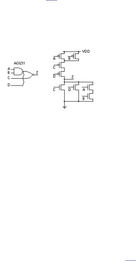
3.10(Euler paths, 60 min.) There are several ways to arrange the stacks in the AOI211 cell shown in Figure 3.25 . For example, the n -channel transistor A can be below B
without altering the function. Which arrangement would you predict gives a faster delay from A to Z and why? The p -channel transistors A and B can be above or below transistors C and D. How many distinct ways of arranging the transistors are there for this cell? What effect do the different arrangements have on layout? What effects do these different arrangements have on the cell performance?
FIGURE 3.25 There are several ways to arrange the transistors in this AOI211 cell (Problem 3.10 ).
3.11 (*AOI and OAI cell efficiency, 60 min.) A standard-cell library data book contains the following data:
●AOI221: t R = 1.06 1.15 ns; t F = 1.09 1.55 ns; C in = 0.21 0.28 pF; W C = 28.8 m m
●OAI221: t R = 0.77 1.05 ns; t F = 0.81 0.96 ns; C in = 0.25 0.39 pF; W C = 22.4 m m
( W C is the cell width, the cell height is 25.6 m m.) Calculate the (a) logical effort and
(b) logical area for the AOI221 and OAI221 cells.
The implementation of the OAI221 in this library uses a single stage,
OAI221 = OAI221(a1, a2, b1, b2, c),
whereas the AOI221 uses the following multistage implementation:
AOI221 = NOT(NAND(NAND(a1, a2), AOI21(b1, b2, c))).
(c) What are the alternative implementations for these two cells? (d) From your answers attempt to explain the implementations chosen.
3.12 (**Logical efficiency, 60 min.) Extending Problem 3.11 , let us compare an AOI33 with an OAI33 cell. (a) Calculate the logical effort and (b) logical areas for these cells.

The AOI33 uses a single-stage implementation as follows:
AOI33 = aoi33(a1, a2, a3, b1, b2, b3).
The OAI33 uses the following multistage implementation:
OAI33 = not[nor[nor(a1, a2, a3), nor(b1, b2, b3)]].
(c) Calculate the path delay, D , as a function of path electrical effort, H , for both of these implementations ignoring parasitic and nonideal delays. (d) Use Eq. 3.42 to
calculate the optimum path delay for these cells. (e) Compare and explain the differences between your answers to parts d and e for H = 1, 2, 4, and 8.
The timing data from the data book is as follows (the cell height is 25.6 m m):
●AOI33: t R = 0.70 1.06 ns; t F = 0.72 1.15 ns; C in = 0.21 0.28 pF; W C = 35.2 m m
●OAI33: t R = 1.06 1.70 ns; t F = 1.42 1.98 ns; C in = 0.31 0.36 pF; W C = 48 m m
(f)How does this data compare with your theoretical analysis?
3.13(EXOR cells and logical effort, 60 min.) Show how to implement a two-input EXOR cell using an AOI22 and two inverters. Using logical effort, compare this with an implementation using an AOI21 cell and a NOR cell.
3.14(***XNOR cells, 60 min.) Table 3.3 shows the implementation of XNOR cells in a standard-cell library. Analyze this data using the concept of logical effort.
TABLE 3.3
Cell
Library 1:
XNOR2D1
Library 2:
XNOR2D1
Library 1:
XNOR2D2
Library 2:
XNOR2D2
Library 1:
XNOR3D1
Library 1:
XNOR3D2
Implementations of XNOR cells in CMOS (Problem 3.14 ).
Implementation
nand[or(a1,a2),nand(a1,a2)]
NOT[NOT[MUX[a1, NOT(a1),a2)]]
NOT[NOT[MUX(a1,NOT(a1),a2)]]
nand[or(a1,a2),nand(a1,a2)]
NOT[NOT[MUX(a1, NOT(a1), NOT(MUX(a3, NOT(a3),a2)))]]
NOT[NOT[MUX(a1, NOT(a1), NOT(MUX(a3, NOT(a3),a2)))]]
3.15 (***Extensions to logical effort, 60 min.) The path branching effort B is the product of branching efforts:
B = |
b i . (3.47) |
i path
The branching effort is the ratio of the on-path plus off-path capacitance to the on-path capacitance. The path effort F becomes the product of the path electrical effort, path branching effort, and path logical effort:
F = GBH . (3.48)
Show that the path delay D is
D = |
g i b i h i + |
p i . (3.49) |
i path |
i path |
|
(***) Show that the optimum path delay is then
D^ = NF 1/ N = N ( GBH ) 1/ N + P . (3.50)
3.16 (*Circuits from layout, 120 min.) Figure 3.26 shows a D flip-flop with clear
from a 1.0 m m standard-cell library. Figure 3.27 shows two layout views of this D
flip-flop. Construct the circuit diagram for this flip-flop, labeling the nodes and transistors as shown. Include the transistor sizes use estimates for transistors with 45° gates you only need W/L values, you can assume the gate lengths are all L = 2 l , equal to the minimum feature size. Label the inputs and outputs to the cell and identify their functions.
FIGURE 3.26 A D flip-flop from a 1.0 m m standard-cell library (Problem 3.16 ).
3.17 (Flip-flop circuits, 30 min.) Draw the circuit schematic for a positive-edgetriggered D flip-flop with active-high set and reset (base your schematic on
Figure 2.18a, a negative-edge triggered D flip-flop). Describe the problem when both SET and RESET are high.

FIGURE 3.27 (Top) A standard cell showing the diffusion ( n -diffusion and p -diffusion), poly, and contact layers (the n -well and p -well are not shown). (Bottom) Shows the m1, contact, m2, and via layers. Problem 3.16 traces this circuit for this cell.
If we want an active-high set or reset we can: (1) use an inverter on the set or reset signal or (2) we can substitute NOR cells. Since NOR cells are slower than NAND cells, which we do depends on whether we want to optimize for speed or area.
Thus, the largest flip-flop would be one with both Q and QN outputs, active high set and reset requiring four TX gates, three inverters (four of the seven we normally need are replaced with NAND cells), four NAND cells, and two inverters to invert the set and reset, making a total of 34 transistors, or 8.5 gates.
3.18(Set and reset, 10 min.) Show how to add a synchronous set or a synchronous reset to the flip-flop of Figure 2.18(a) using a two-input MUX.
3.19(Clocked inverters, 45 min.) Using PSpice compare the delay of an inverter with transmission gate with that of a clocked inverter using the G5 process SPICE parameters from Table 2.1.

3.20 (S-R, T, J-K flip-flops, 30 min.) The characteristic equation for a D flip-flop is Q t+1 = D. The characteristic equation for a J-K flip-flop is Q t+1 = J(Q t )' + K'Q t .
●a. Show how you can build a J-K flip-flop using a D flip-flop.
●b. The characteristic equation for a T flip-flop (toggle flip-flop) is Q t+1 = (Q t )' . Show how to build a T flip-flop using a D flip-flop.
●c. The characteristic equation does not show the timing behavior of a sequential element the characteristic equation for a D latch is the same as that for a D flip-flop. The characteristic equation for an S-R latch and an S-R flip-flop is Q t+1 = S + R'Q t . An S-R flip-flop is sometimes called a pulse-triggered flip-flop.
Find out the behavior of an S-R latch and an S-R flip-flop and describe the differences between these elements and a D latch and a D flip-flop.
●d. Explain why it is probably not a good idea to use an S-R flip-flop in an ASIC design.
3.21(**Optimum logic, 60 min.) Suppose we have a fixed logic path of length n 1 .
We want to know how many (if any) buffer stages we should add at the output of this path to optimize the total path delay given the output load capacitance.
●a. If the total number of stages is N (logic path of length n 1 plus N n 1 inverters), show that the total path delay is
n 1
D^ = NF 1/ N + ( p i + q i ) + ( N n 1 )( p inv + q inv ) . (3.51) i = 1
The optimum number of stages is given by the solution to the following equation:
D^/ N= / N ( NF 1/ N + ( N n 1 )( p inv + q inv ) ) = 0 . (3.52)
●b. Show that the solutions to this equation can be written in terms of F 1/ N^ (the optimum stage effort) where N^ is the optimum number of stages:
F 1/ N^ (1 ln F 1/ N^ ) + ( p inv + q inv ) = 0 . (3.53)
3.22 (XOR and XNOR cells, 60 min.) Table 3.4 shows the implementations of two-
and three-input XOR cells in an ASIC standard-cell library (D1 are the 1X drive cells, and D2 are the 2X drive versions). Can you explain the choices for the two-input XOR cell and complete the table for the three-input XOR cell?
TABLE 3.4 Implementations of XOR cells (Problem 3.22 ).
Cell |
Actual implementation 1 |
Alternative implementation(s) |
XOR2D1 AOI21[a1, a2, NOR(a1,a2)] |
not[mux(a1, not(a1), a2)] |
|
|
|
aoi22(a1, a2, not(a1), not(a2)) |
XOR2D2 NOT[MUX(a1, not(a1), a2)] |
aoi21[a1, a2, nor(a1, a2)] |
|
|
|
aoi22(a1, a2, not(a1), not(a2)) |
XOR3D1 NOT[MUX[a1,a2))]] not(a1), not(mux(a3, not(a3), ?
XOR3D2 NOT[MUX[a1,a2))]] not(a1), not(mux(a3, not(a3), ?
3.23 (Library density, 10 min.) Derive an upper limit on cell density as follows: Assume a chip consists only of two-input NAND cells with no routing channels between rows (often achievable in a 3LM process with over-the-cell routing).
●a. Explain how many vertical tracks you need to connect to a two-input NAND cell, assuming each connection requires a separate track.
●b. If the NAND cell is 64 l high with a vertical track width of 8 l , calculate the NAND cell area, carefully explaining any assumptions.
●c. Calculate the cell density (in gate/mil 2 ) for a 0.35 m m process, l = 0.175 m m.
Answer: 3 tracks, 47 m m 2 , 13.7 gates/mil 2 or 21 ¥ 103 gates/mm 2 .
3.24(Gate-array density, 20 min.) The LSI Logic 10k and 100k gate arrays use a four-transistor base cell, equivalent to 1 gate, that is 12 tracks high and 3 tracks wide.
●a. If a metal track is 8l, where l = 0.75 m m for a 1.5 m m technology, calculate the area of the LSI Logic base cell A L in mil 2 .
●b. If we could use every base cell in the gate array, the cell density would be D G = 1/ A L . Assume that, because of routing area and inefficiency of the gate array, we can use only 50 percent of the base cells for logic. What is D G for the LSI Logic 1.5 m m array?
●c. Chip cell density D G is about 1.0 gate/mil 2 for a 1 m m technology (a two-input NAND cell occupies an area 25 m m on a side in a technology whose transistors are 1 m m long). This can change by a factor of 2 or more for a gate-array/standard-cell ASIC or high-density/high-performance library. Assume that cell density D G scales ideally with technology. If the minimum feature size of a technology is 2l, then D G 1/ l 2 . Thus, for example, a 1.5 m m technology should have a cell density of roughly (1/1.5) 2 gates/mil 2 . How does this agree with your estimate for the LSI Logic array?
3.25(SiArc RAM, 10 min.) Suppose we need 16 k-bit of SRAM and 20 k-gate of random logic on a channelless gate array. Assume a base cell with four transistors and that we can build a RAM cell using two of these base cells. The RAM bits will require 32k base cells and the random logic will require 20k base cells. Suppose the base cell area is 12 tracks high, 3 tracks wide, and the horizontal and vertical track spacing is equal at 8 l .
●a. Calculate the total area of the base cells we need. Now suppose we redesign the gate-array base cell so that we can build a RAM bit cell using a single base cell that is 20 tracks high, 3 tracks wide, and has 4 logic cell transistors and 4 RAM cell transistors. Assume that since the base cell now contains 8 transistors we only need 12 k base cells to implement 20 k-gate of random logic (the new base cell is less efficient than the old cell for implementing random logic).
●b. Calculate the base cell area using the new base cell design.
●c. Comment.
Answer: 1.2 ¥ 108 l 2 , 1.1 ¥ 108 l 2 .
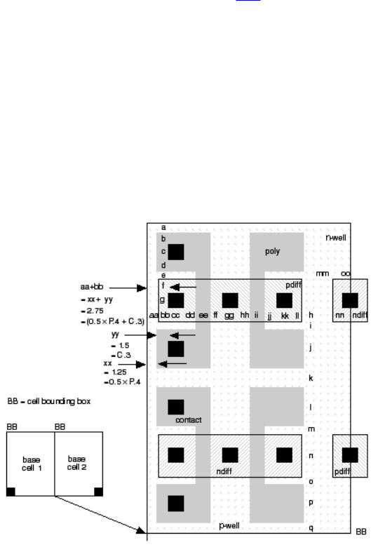
3.26 (***Gate-array base cell, 60 min.) Figure 3.28 shows a simple gate-array base
cell. Use the design rules shown in Table 2.16 (Problem 2.33) to calculate the minimum size of this base cell. Do this by determining which design rules apply to the labels shown adjacent to each space or width in the figure. In most cases each of the spaces is determined by a single rule related to the region labeled, for example, the contact width labeled 'cc' is 2 l determined by rule C.1, the exact contact size. There is one exception, shown in the figure. Space 'aa' (bounding box, BB, to edge of pdiff) and width 'bb' (edge of pdiff to edge of contact) are determined by the minimum space labeled 'xx' (bounding box, BB, to poly edge) and width 'yy' (edge of poly to edge of contact). Space 'xx' is one half of the poly to poly spacing over field (rule P.4) because two base cells abut as shown in the figure. Width 'yy' is equal to the minimum poly overlap of contact (rule C.3). The distance 'aa + bb' is thus determined by the minimum distance 'xx + yy', as shown. The other distances are more straightforward to determine.
Answer: 40 l high by 26.25 l wide.
FIGURE 3.28 A simple gate-array base cell (Problem 3.26 ).
3.27 (CIF, 15 min.) Here is the part of the CIF for a standard cell that describes the n -well (CWN) and p -well (CWP) structure. The statement B length height xCenter,

yCenter is CIF for a box (CIF dimensions are in centimicrons, 0.01 m m):
DS1;LCWN;B6000
1560 13600,3660;B2480 60 11840,2850;B2320 60 15440,2850;LCWP;B680 60
13740,2730;B6000 1380 13600,2010;
●a. Draw the wells and BB. Label the dimensions in microns and l (l = 0.4 m m ) .
●b. This is a double-entry cell with m2 connectors at top and bottom. For this cell library the cell AB is 3 l (120 centimicrons, determined by the well rules) inside the cell BB on all sides. What is the size of the cell AB in microns and l ?
●c. The vertical (m2) routing pitch (the distance between centers of adjacent vertical m2 interconnect lines) is equal to the vertical track spacing and is 8 l (320 centimicrons). How many vertical tracks are there in this cell?
3.28(CIF, 60 min.) Figure 3.29 shows an example of CIF that describes a single rectangle (box) of m1 with an accompanying label.
(CIF written by the Tanner Research layout editor: L-Edit); (TECHNOLOGY: VLSIcmn6);
(DATE: Thu, Jun 27, 1996); (FABCELL: NONE);
(SCALING: 1 CIF Unit = 1/120 Lambda, 1 Lambda = 3/10 Microns);
DS1 2 8;
9 Cell0;
94 LabelText 60 180 CM; LCM;
B 240 120 120 300; DF;
E
FIGURE 3.29 A simple CIF example (Problem 3.28 ).
The CIF code has the following meaning:
●Lines 1 5 are CIF comments.
●Line 6 is a definition start for symbol 1 and marks the beginning of a symbol definition (a symbol is a piece of layout, symbol numbers are unique identifiers). The integers 2 and 8 define a scaling factor 2/8 (= 0.25) to be applied to distance measurements (the CIF unit, after scaling, is a centimicron or 0.01 m m).
●Line 7 is a user extension or expansion (all extensions begin with a digit). L-Edit uses user extension 9 for cell names ( Cell0 in this case).
●Line 8 is a user extension for a cell label located on layer CM (first-level metal in this technology) located at x = 60 units, y = 180 units (60, 180). Applying the scaling factor of 0.25, this translates to (15, 45) in centimicrons or (0.5, 1.5) in lambda.
●Line 9 is a layer specification or command (begins with L ).
●Line 10 is a box command and describes a box with (in order) length, L , of 240 units; width, W , of 120 units; and center at x = 120 units and y = 300 units.

Applying the DS scaling factor of 0.25 gives L = 60, W = 30, center = (30, 75)(centimicrons) or L = 2, W = 1, center = (1, 2.5) in lambda.
●Line 11 is the definition finish ( DS and DF must be paired).
●Line 12 is the end command .
You receive a CIF file whose mask-layer names are different from those in the technology file that you are using. The mapping between layer names is shown in Table 3.5 .
●a. Write an awk or sed script (or use another automated editing technique) to change the layer names. At this point you realize that there are several layer names ( LTRAN , LESD ) in the input file that are not required (or recognized) by your layout software (these particular examples are for software to recognize unused transistors in a gate array, and for an ESD implant in I/O devices).
●b. (**) Enhance your script to completely remove an unwanted layer from the CIF file. There are some comments and CIF constructs that are not supported by your editor. Here is one example:
(BB: 39.2,82.6 72.8,122.5 in lambda);
Comments in this format specify the AB and BB for the cell. Other CIF user extensions, not recognized by your software, are used for labels for power supplies and connectors:
4A 1680 3360 2800 4844;
4M a 1 2292 4028 2356 4092 CM2;
4M z 4 2639 4090 2703 4154 CM2;
4X vdd 2 2800 4774 180 * * metal;
● c. (**) Add code to remove all these constructs from the CIF file.
TABLE 3.5 Mapping CIF layer names (Problem 3.28 ). 2
Input mask |
MOSIS mask Input mask |
MOSIS mask Input mask MOSIS mask |
||||||||
label |
label |
label |
label |
label |
label |
|||||
LCNW |
CWN |
LCND 3 |
CSN |
LCM2 |
CMS |
|||||
|
|
|
|
|
|
|
|
|
|
|
LCPW |
CWP |
LCPD 2 |
CSP |
LCC2 |
CVS |
|||||
none 4 |
CAA |
LCC 5 |
CCA |
LCM3 |
CMT |
|||||
|
|
|
|
|
|
|
|
|
|
|
LCP |
|
|
CPG |
LCM |
CMF |
none |
COG |
|||
1.MUX(a, b, c) = a·c + b·c'
2.This mapping is for input to a layout editor; the CIF may have to be modified again when written out from the layout editor.
3.Map the input diffusion layers to the implant select layers. On output from the layout editor these layers should be sized up to generate the real implant select layers.
4.There is no active layer in the input. Instead use the diffusion layers.
5.There is only one contact layer in the input; map all contacts to CAA.There is no easy way to generate the MOSIS CCP layer. This prevents handling of poly and