

7.1 Actel ACT
The Actel ACT family interconnect scheme shown in Figure 7.1 is similar to a channeled gate array. The channel routing uses dedicated rectangular areas of fixed size within the chip called wiring channels (or just channels ). The horizontal channels run across the chip in the horizontal direction. In the vertical direction there are similar vertical channels that run over the top of the basic logic cells, the Logic Modules. Within the horizontal or vertical channels wires run horizontally or vertically, respectively, within tracks . Each track holds one wire. The capacity of a fixed wiring channel is equal to the number of tracks it contains. Figure 7.2 shows a detailed view of the channel and the connections to each Logic Module the input stubs and output stubs .
FIGURE 7.1 The interconnect architecture used in an Actel ACT family FPGA. ( Source: Actel.)

FIGURE 7.2 ACT 1 horizontal and vertical channel architecture. (Source: Actel.)
In a channeled gate array the designer decides the location and length of the interconnect within a channel. In an FPGA the interconnect is fixed at the time of manufacture. To allow programming of the interconnect, Actel divides the fixed interconnect wires within each channel into various lengths or wire segments. We call this segmented channel routing, a variation on channel routing. Antifuses join the wire segments. The designer then programs the interconnections by blowing antifuses and making connections between wire segments; unwanted connections are left unprogrammed. A statistical analysis of many different layouts determines the optimum number and the lengths of the wire segments.
7.1.1 Routing Resources
The ACT 1 interconnection architecture uses 22 horizontal tracks per channel for signal routing with three tracks dedicated to VDD, GND, and the global clock (GCLK), making a total of 25 tracks per channel. Horizontal segments vary in length from four columns of Logic Modules to the entire row of modules (Actel calls these long segments long lines ).
Four Logic Module inputs are available to the channel below the Logic Module and four inputs to the channel above the Logic Module. Thus eight vertical tracks per Logic Module are available for inputs (four from the Logic Module above the channel and four from the Logic Module below). These connections are the input
stubs.
The single Logic Module output connects to a vertical track that extends across the two channels above the module and across the two channels below the module. This is the output stub. Thus module outputs use four vertical tracks per module (counting two tracks from the modules below, and two tracks from the modules above each channel). One vertical track per column is a long vertical track ( LVT ) that spans the entire height of the chip (the 1020 contains some segmented LVTs). There are thus a total of 13 vertical tracks per column in the ACT 1 architecture (eight for inputs, four for outputs, and one for an LVT).
Table 7.1 shows the routing resources for both the ACT 1 and ACT 2 families. The last two columns show the total number of antifuses (including antifuses in the I/O cells) on each chip and the total number of antifuses assuming the wiring channels are fully populated with antifuses (an antifuse at every horizontal and vertical interconnect intersection). The ACT 1 devices are very nearly fully populated.
TABLE 7.1 Actel FPGA routing resources.
|
|
Total |
Horizontal |
Vertical |
Rows, R Columns, C antifuses |
tracks per |
tracks per |
|
channel, H |
column, V |
on each |
|
|
chip |
H ¥ V ¥ R ¥ C
A1010 |
22 |
13 |
8 |
44 |
112,000 |
100,672 |
A1020 |
22 |
13 |
14 |
44 |
186,000 |
176,176 |
A1225A 36 |
15 |
13 |
46 |
250,000 |
322,920 |
|
A1240A 36 |
15 |
14 |
62 |
400,000 |
468,720 |
|
A1280A 36 |
15 |
18 |
82 |
750,000 |
797,040 |
|
If the Logic Module at the end of a net is less than two rows away from the driver module, a connection requires two antifuses, a vertical track, and two horizontal segments. If the modules are more than two rows apart, a connection between them will require a long vertical track together with another vertical track (the output stub) and two horizontal tracks. To connect these tracks will require a total of four antifuses in series and this will add delay due to the resistance of the antifuses. To examine the extent of this delay problem we need some help from the analysis of RC networks.
7.1.2 Elmore s Constant
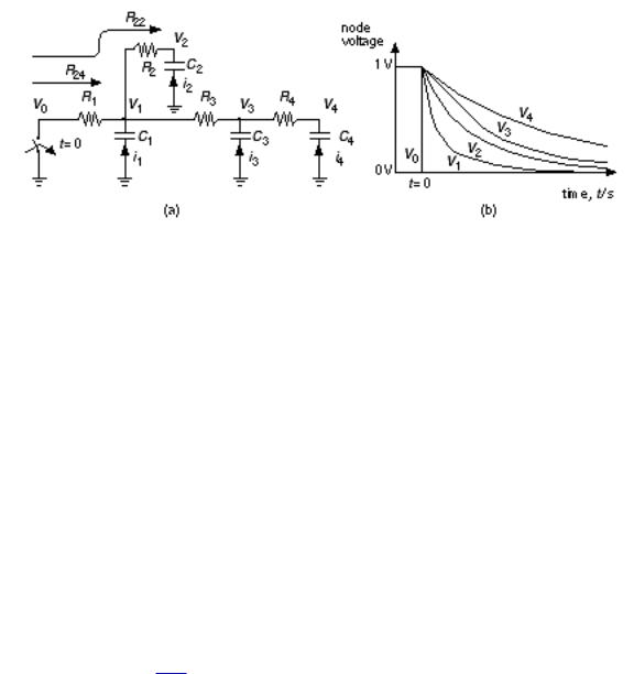
Figure 7.3 shows an RC tree representing a net with a fanout of two. We shall assume that all nodes are initially charged to V DD = 1 V, and that we short node 0 to ground, so V 0 = 0 V, at time t = 0 sec. We need to find the node voltages, V 1 to V 4 , as a function of time. A similar problem arose in the design of
wideband vacuum tube distributed amplifiers in the 1940s. Elmore found a measure of delay that we can use today [ Rubenstein, Penfield, and Horowitz, 1983].
FIGURE 7.3 Measuring the delay of a net. (a) An RC tree. (b) The waveforms as a result of closing the switch at t = 0.
The current in branch k of the network is
d V k
i k = C k . (7.1) d t
The linear superposition of the branch currents gives the voltage at node i as
n |
d V k |
V i = S |
R ki C k , (7.2) |
k = 1 |
d t |
where R ki is the resistance of the path to V 0 (ground in this case) shared by node k and node i . So, for example, R 24 = R 1 , R 22 = R 1 + R 2 , and R 31 = R 1 .
Unfortunately, Eq. 7.2 is a complicated set of coupled equations that we cannot
easily solve. We know the node voltages have different values at each point in time, but, since the waveforms are similar, let us assume the slopes (the time derivatives) of the waveforms are related to each other. Suppose we express the slope of node voltage V k as a constant, a k , times the slope of V i ,
d V k |
d V i |
|
= a k . (7.3) |
d t |
d t |
Consider the following measure of the error, E , of our approximation:
n

E = S R ki C k . (7.4) k = 1
The error, E , is a minimum when a k = 1 since initially V i ( t = 0) = V k ( t = 0) = 1 V (we normalized the voltages) and V i ( t = " ) = V k ( t = " ) = 0.
Now we can rewrite Eq. 7.2 , setting a k = 1, as follows:
n |
d V i |
V i = S |
R ki C k , (7.5) |
k = 1 |
d t |
This is a linear first-order differential equation with the following solution:
n |
|
V i ( t ) = exp ( t / t Di ) ; t Di = S |
R ki C k . (7.6) |
k = 1
The time constant t D i is often called the Elmore delay and is different for each node. We shall refer to t D i as the Elmore time constant to remind us that, if we approximate V i by an exponential waveform, the delay of the RC tree using 0.35/0.65 trip points is approximately t Di seconds.
7.1.3 RC Delay in Antifuse Connections
Suppose a single antifuse, with resistance R 1 , connects to a wire segment with parasitic capacitance C 1 . Then a connection employing a single antifuse will delay the signal passing along that connection by approximately one time constant, or R 1 C 1 seconds. If we have more than one antifuse, we need to use the Elmore time constant to estimate the interconnect delay.
FIGURE 7.4 Actel routing model. (a) A four-antifuse connection. L0 is an output stub, L1 and L3 are horizontal tracks, L2 is a long vertical track (LVT), and L4 is an input stub. (b) An RC-tree model. Each antifuse is modeled by a resistance and each interconnect segment is modeled by a capacitance.

For example, suppose we have the four-antifuse connection shown in Figure 7.4 . Then, from Eq. 7.6 ,
t D 4 = R 14 C 1 + R 24 C 2 + R 14 C 1 + R 44 C 4
(R 1 + R 2 + R 3 + R 4 ) C 4 + (R 1 + R 2 + R 3 ) C 3 + (R 1 + R 2 ) C 2 + = R 1 C 1
If all the antifuse resistances are approximately equal (a reasonably good assumption) and the antifuse resistance is much larger than the resistance of any of the metal lines, L1 L5, shown in Figure 7.4 (a very good assumption) then R 1 = R 2 = R 3 = R 4 = R , and the Elmore time constant is
t D 4 = 4 RC 4 + 3 RC 3 + 2 RC 2 + RC 1 (7.7)
Suppose now that the capacitance of each interconnect segment (including all the antifuses and programming transistors that may be attached) is approximately constant, and equal to C . A connection with two antifuses will generate a 3 RC time constant, a connection with three antifuses a 6 RC time constant, and a connection with four antifuses gives a 10 RC time constant. This analysis is disturbing it says that the interconnect delay grows quadratically ( n2 ) as we increase the interconnect length and the number of antifuses, n . The situation is worse when the intermediate wire segments have larger capacitance than that of the short input stubs and output stubs. Unfortunately, this is the situation in an Actel FPGA where the horizontal and vertical segments in a connection may be quite long.
7.1.4 Antifuse Parasitic Capacitance
We can determine the number of antifuses connected to the horizontal and vertical lines for the Actel architecture. Each column contains 13 vertical signal tracks and each channel contains 25 horizontal tracks (22 of these are used for signals). Thus, assuming the channels are fully populated with antifuses,
●An input stub (1 channel) connects to 25 antifuses.
●An output stub (4 channels) connects to 100 (25 ¥ 4) antifuses.
●An LVT (1010, 8 channels) connects to 200 (25 ¥ 8) antifuses.
●An LVT (1020, 14 channels) connects to 350 (25 ¥ 14) antifuses.
●A four-column horizontal track connects to 52 (13 ¥ 4) antifuses.
●A 44-column horizontal track connects to 572 (13 ¥ 44) antifuses.
A connection to the diffusion of an Actel antifuse has a parasitic capacitance due to the diffusion junction. The polysilicon of the antifuse has a parasitic capacitance due to the thin oxide. These capacitances are approximately equal. For a 2 m m CMOS process the capacitance to ground of the diffusion is 200 to 300 aF m m 2 (area component) and 400 to 550 aF m m 1 (perimeter
component). Thus, including both area and perimeter effects, a 16 m m 2 diffusion contact (consisting of a 2 m m by 2 m m opening plus the required overlap) has a parasitic capacitance of 10 14 f F. If we assume an antifuse has a parasitic capacitance of approximately 10 fF in a 1.0 or 1.2 m m process, we can calculate the parasitic capacitances shown in Table 7.2 .
TABLE 7.2 Actel interconnect parameters. |
|
||
Parameter |
A1010/A1020 |
A1010B/A1020B |
|
Technology |
2.0 m m, l = 1.0 m m |
1.2 m m, l = 0.6 m m |
|
Die height (A1010) |
240 mil |
144 mil |
|
Die width (A1010) |
360 mil |
216 mil |
|
Die area (A1010) |
86,400 mil 2 = 56 M l 2 |
31,104 mil 2 = 56 M l 2 |
|
Logic Module (LM) |
180 m m = 180 l |
108 m m = 180 l |
|
height (Y1) |
|||
|
|
||
LM width (X) |
150 m m = 150 l |
90 m m = 150 l |
|
LM area (X ¥ Y1) |
27,000 m m 2 = 27 k l 2 |
9,720 m m 2 = 27 k l 2 |
|
Channel height (Y2) |
25 tracks = 287 m m |
25 tracks = 170 m m |
|
Channel area per LM |
43,050 m m 2 = 43 k l 2 |
15,300 m m 2 = 43 k l 2 |
|
(X ¥ Y2) |
|
|
|
LM and routing area |
70,000 m m 2 = 70 k l 2 |
25,000 m m 2 = 70 k l 2 |
|
(X ¥ Y1 + X ¥ Y2) |
|
|
|
Antifuse capacitance |
|
10 fF |
|
Metal capacitance |
0.2 pFmm 1 |
0.2 pFmm 1 |
|
Output stub length |
|
|
|
(spans 3 LMs + 4 |
4 channels = 1688 m m |
4 channels = 1012 m m |
|
|
|
||
channels) |
|
|
|
Output stub metal |
0.34 pF |
0.20 pF |
|
capacitance |
|||
|
|
||
Output stub antifuse |
100 |
100 |
|
connections |
|||
|
|
||
Output stub antifuse |
|
1.0 pF |
|
capacitance |
|||
|
|
||
Horiz. track length |
4 44 cols. = 600 6600 m |
4 44 cols. = 360 3960 m m |
|
|
m |
|
|
Horiz. track metal |
0.1 1.3 pF |
0.07 0.8 pF |
|
capacitance |
|||
|
|
||
Horiz. track antifuse |
52 572 antifuses |
52 572 antifuses |
|
connections |
|
|
|
Horiz. track antifuse |
|
0.52 5.72 pF |
|
capacitance |
|
|
|

Long vertical track |
8 14 channels = 3760 |
8 14 channels = 2240 3920 m m |
|
(LVT) |
6580 m m |
||
|
|||
LVT metal |
0.08 0.13 pF |
0.45 0.8 pF |
|
capacitance |
|||
|
|
||
LVT track antifuse |
200 350 antifuses |
200 350 antifuses |
|
connections |
|||
|
|
||
LVT track antifuse |
|
2 3.5 pF |
|
capacitance |
|
||
|
|
||
Antifuse resistance |
|
0.5 k W (typ.), 0.7 k W (max.) |
|
(ACT 1) |
|
||
|
|
We can use the figures from Table 7.2 to estimate the interconnect delays. First we calculate the following resistance and capacitance values:
1.The antifuse resistance is assumed to be R = 0.5 k W .
2.C 0 = 1.2 pF is the sum of the gate output capacitance (which we shall neglect) and the output stub capacitance (1.0 pF due to antifuses, 0.2 pF due to metal). The contribution from this term is zero in our calculation because we have neglected the pull resistance of the driving gate.
3.C 1 = C 3 = 0.59 pF (0.52 pF due to antifuses, 0.07 pF due to metal) corresponding to a minimum-length horizontal track.
4.C 2 = 4.3 pF (3.5 pF due to antifuses, 0.8 pF due to metal) corresponding to a LVT in a 1020B.
5.The estimated input capacitance of a gate is C 4 = 0.02 pF (the exact value will depend on which input of a Logic Module we connect to).
From Eq. 7.7 , the Elmore time constant for a four-antifuse connection is
tD 4 = 4(0.5)(0.02) + 3(0.5)(0.59) + 2(0.5)(4.3) + (0.5)(0.59) (7.8)
=5.52 ns .
This matches delays obtained from the Actel delay calculator. For example, an LVT adds between 5 10 ns delay in an ACT 1 FPGA (6 12 ns for ACT 2, and 414 ns for ACT 3). The LVT connection is about the slowest connection that we can make in an ACT array. Normally less than 10 percent of all connections need to use an LVT and we see why Actel takes great care to make sure that this is the case.
7.1.5 ACT 2 and ACT 3 Interconnect
The ACT 1 architecture uses two antifuses for routing nearby modules, three antifuses to join horizontal segments, and four antifuses to use a horizontal or vertical long track. The ACT 2 and ACT 3 architectures use increased interconnect resources over the ACT 1 device that we have described. This

reduces further the number of connections that need more than two antifuses. Delay is also reduced by decreasing the population of antifuses in the channels, and by decreasing the antifuse resistance of certain critical antifuses (by increasing the programming current).
The channel density is the absolute minimum number of tracks needed in a channel to make a given set of connections (see Section 17.2.2, Measurement of Channel Density ). Software to route connections using channeled routing is so efficient that, given complete freedom in location of wires, a channel router can usually complete the connections with the number of tracks equal or close to the theoretical minimum, the channel density. Actel s studies on segmented channel routing have shown that increasing the number of horizontal tracks slightly (by approximately 10 percent) above density can lead to very high routing completion rates.
The ACT 2 devices have 36 horizontal tracks per channel rather than the 22 available in the ACT 1 architecture. Horizontal track segments in an ACT 3 device range from a module pair to the full channel length. Vertical tracks are: input (with a two channel span: one up, one down); output (with a four-channel span: two up, two down); and long (LVT). Four LVTs are shared by each column pair. The ACT 2/3 Logic Modules can accept five inputs, rather than four inputs for the ACT 1 modules, and thus the ACT 2/3 Logic Modules need an extra two vertical tracks per channel. The number of tracks per column thus increases from 13 to 15 in the ACT 2/3 architecture.
The greatest challenge facing the Actel FPGA architects is the resistance of the polysilicon-diffusion antifuse. The nominal antifuse resistance in the ACT 1 2 1 2 m m processes (with a 5 mA programming current) is approximately 500 W and, in the worst case, may be as high as 700 W . The high resistance severely limits the number of antifuses in a connection. The ACT 2/3 devices assign a special antifuse to each output allowing a direct connection to an LVT. This reduces the number of antifuses in a connection using an LVT to three. This type of antifuse (a fast fuse) is blown at a higher current than the other antifuses to give them about half the nominal resistance (about 0.25 k W for AC T 2) of a normal antifuse. The nominal antifuse resistance is reduced further in the ACT 3 (using a 0.8 m m process) to 200 W (Actel does not state whether this value is for a normal or fast fuse). However, it is the worst-case antifuse resistance that will determine the worst-case performance.