- •INTRODUCTION TO ASICs
- •1.1 Types of ASICs
- •1.2 Design Flow
- •1.3 Case Study
- •1.4 Economics of ASICs
- •1.5 ASIC Cell Libraries
- •1.6 Summary
- •1.7 Problems
- •1.8 Bibliography
- •1.9 References
- •CMOS LOGIC
- •2.12 References
- •2.1 CMOS Transistors
- •2.2 The CMOS Process
- •2.3 CMOS Design Rules
- •2.4 Combinational Logic Cells
- •2.5 Sequential Logic Cells
- •2.6 Datapath Logic Cells
- •2.7 I/O Cells
- •2.8 Cell Compilers
- •2.9 Summary
- •2.10 Problems
- •2.11 Bibliography
- •ASIC LIBRARY DESIGN
- •3.1 Transistors as Resistors
- •3.3 Logical Effort
- •3.4 Library-Cell Design
- •3.5 Library Architecture
- •3.6 Gate-Array Design
- •3.7 Standard-Cell Design
- •3.8 Datapath-Cell Design
- •3.9 Summary
- •3.10 Problems
- •3.11 Bibliography
- •3.12 References
- •PROGRAMMABLE ASICs
- •4.1 The Antifuse
- •4.2 Static RAM
- •4.4 Practical Issues
- •4.5 Specifications
- •4.6 PREP Benchmarks
- •4.7 FPGA Economics
- •4.8 Summary
- •4.9 Problems
- •4.10 Bibliography
- •4.11 References
- •5.1 Actel ACT
- •5.2 Xilinx LCA
- •5.3 Altera FLEX
- •5.4 Altera MAX
- •5.5 Summary
- •5.6 Problems
- •5.7 Bibliography
- •5.8 References
- •6.1 DC Output
- •6.2 AC Output
- •6.3 DC Input
- •6.4 AC Input
- •6.5 Clock Input
- •6.6 Power Input
- •6.7 Xilinx I/O Block
- •6.8 Other I/O Cells
- •6.9 Summary
- •6.10 Problems
- •6.11 Bibliography
- •6.12 References
- •7.1 Actel ACT
- •7.2 Xilinx LCA
- •7.3 Xilinx EPLD
- •7.4 Altera MAX 5000 and 7000
- •7.5 Altera MAX 9000
- •7.6 Altera FLEX
- •7.7 Summary
- •7.8 Problems
- •7.9 Bibliography
- •7.10 References
- •8.1 Design Systems
- •8.2 Logic Synthesis
- •8.3 The Halfgate ASIC
- •8.3.4 Comparison
- •8.4 Summary
- •8.5 Problems
- •8.6 Bibliography
- •8.7 References
- •9.1 Schematic Entry
- •9.3 PLA Tools
- •9.4 EDIF
- •9.5 CFI Design Representation
- •9.6 Summary
- •9.7 Problems
- •9.8 Bibliography
- •9.9 References
- •VHDL
- •10.1 A Counter
- •10.2 A 4-bit Multiplier
- •10.3 Syntax and Semantics of VHDL
- •10.5 Entities and Architectures
- •10.6 Packages and Libraries
- •10.7 Interface Declarations
- •10.8 Type Declarations
- •10.9 Other Declarations
- •10.10 Sequential Statements
- •10.11 Operators
- •10.12 Arithmetic
- •10.13 Concurrent Statements
- •10.14 Execution
- •10.15 Configurations and Specifications
- •10.16 An Engine Controller
- •10.17 Summary
- •10.18 Problems
- •10.19 Bibliography
- •10.20 References
- •IEEE Language Reference Manual project
- •VERILOG HDL
- •11.1 A Counter
- •11.2 Basics of the Verilog Language
- •11.3 Operators
- •11.4 Hierarchy
- •11.5 Procedures and Assignments
- •11.6 Timing Controls and Delay
- •11.7 Tasks and Functions
- •11.8 Control Statements
- •11.9 Logic-Gate Modeling
- •11.10 Modeling Delay
- •11.11 Altering Parameters
- •11.12 A Viterbi Decoder
- •11.13 Other Verilog Features
- •11.14 Summary
- •11.15 Problems
- •11.16 Bibliography
- •11.17 References
- •12.2 A Comparator/MUX
- •12.3 Inside a Logic Synthesizer
- •12.6 VHDL and Logic Synthesis
- •12.8 Memory Synthesis
- •12.9 The Multiplier
- •12.10 The Engine Controller
- •12.13 Summary
- •12.14 Problems
- •12.15 Bibliography
- •12.16 References
- •SIMULATION
- •13.1 Types of Simulation
- •13.3 Logic Systems
- •13.4 How Logic Simulation
- •13.5 Cell Models
- •13.6 Delay Models
- •13.7 Static Timing Analysis
- •13.8 Formal Verification
- •13.9 Switch-Level Simulation
- •13.11 Summary
- •13.12 Problems
- •13.13 Bibliography
- •13.14 References
- •TEST
- •14.1 The Importance of Test
- •14.2 Boundary-Scan Test
- •14.3 Faults
- •14.4 Fault Simulation
- •14.6 Scan Test
- •14.7 Built-in Self-test
- •14.8 A Simple Test Example
- •14.10 Summary
- •14.11 Problems
- •14.12 Bibliography
- •14.13 References
- •15.1 Physical Design
- •15.3 System Partitioning
- •15.4 Estimating ASIC Size
- •15.5 Power Dissipation
- •15.6 FPGA Partitioning
- •15.7 Partitioning Methods
- •15.8 Summary
- •15.9 Problems
- •15.10 Bibliography
- •15.11 References
- •16.1 Floorplanning
- •16.2 Placement
- •16.3 Physical Design Flow
- •16.4 Information Formats
- •16.5 Summary
- •16.6 Problems
- •16.7 Bibliography
- •16.8 References
- •ROUTING
- •17.1 Global Routing
- •17.2 Detailed Routing
- •17.3 Special Routing
- •17.5 Summary
- •17.6 Problems
- •17.7 Bibliography
- •17.8 References
- •A.2 VHDL Syntax
- •A.3 BNF Index
- •A.5 References
- •B.2 Verilog HDL Syntax
- •B.3 BNF Index
- •B.4 Verilog HDL LRM
- •B.5 Bibliography
- •B.6 References
15.3 System Partitioning
Microelectronic systems typically consist of many functional blocks. If a functional block is too large to fit in one ASIC, we may have to split, or partition, the function into pieces using goals and objectives that we need to specify. For example, we might want to minimize the number of pins for each ASIC to minimize package cost. We can use CAD tools to help us with this type of system partitioning.
Figure 15.2 shows the system diagram of the Sun Microsystems SPARCstation 1. The system is partitioned as follows; the numbers refer to the labels in
Figure 15.2 . (See Section 1.3, Case Study for the sources of infomation in this section.)
●Nine custom ASICs (1 9)
●Memory subsystems (SIMMs, single-in-line memory modules): CPU cache (10), RAM (11), memory cache (12, 13)
●Six ASSPs (application-specific standard products) for I/O (14 19)
●An ASSP for time of day (20)
●An EPROM (21)
●Video memory subsystem (22)
●One analog/digital ASSP DAC (digital-to-analog converter) (23)
Table 15.1 shows the details of the nine custom ASICs used in the SPARCstation 1. Some of the partitioning of the system shown in Figure 15.2 is determined by whether to use ASSPs or custom ASICs. Some of these design
decisions are based on intangible issues: time to market, previous experience with a technology, the ability to reuse part of a design from a previous product. No CAD tools can help with such decisions. The goals and objectives are too poorly defined and finding a way to measure these factors is very difficult. CAD tools cannot answer a question such as: What is the cheapest way to build my system? but can help the designer answer the question: How do I split this circuit into pieces that will fit on a chip? Table 15.2 shows the partitioning of the SPARCstation 10 so you can compare it to the SPARCstation 1. Notice that the gate counts of nearly all of the SPARCstation 10 ASICs have increased by a factor of 10, but the pin counts have increased by a smaller factor.
FIGURE 15.2 The Sun Microsystems SPARCstation 1 system block diagram. The acronyms for the various ASICs are listed in Table 15.1 .
TABLE 15.1 System partitioning for the Sun Microsystems SPARCstation 1.
SPARCstation 1 ASIC |
Gates |
|
Package |
Type |
|
/k-gate |
Pins |
||||
|
|
|
|||
1 SPARC IU (integer unit) |
20 |
179 |
PGA |
CBIC |
|
2 SPARC FPU (floating-point unit) |
50 |
144 |
PGA |
FC |
|
3 Cache controller |
9 |
160 |
PQFP |
GA |
|
4 MMU (memory-management unit) |
5 |
120 |
PQFP |
GA |
|
5 Data buffer |
3 |
120 |
PQFP |
GA |
|
6 DMA (direct memory access) |
9 |
120 |
PQFP |
GA |
|
controller |
|
|
|
|
|
7 Video controller/data buffer |
4 |
120 |
PQFP |
GA |
|
8 RAM controller |
1 |
100 |
PQFP |
GA |
|
9 Clock generator |
1 |
44 |
PLCC |
GA |
|
Abbreviations: |
|
|
|
|
|
PGA = pin-grid array |
CBIC = LSI Logic cell-based ASIC |
||||
PQFP = plastic quad flat pack |
GA = LSI Logic channelless gate array |
||||
PLCC = plastic leaded chip carrier |
FC = full custom |
|
|
15.4 Estimating ASIC Size
Table 15.3 shows some useful numbers for estimating ASIC die size. Suppose we wish to estimate the die size of a 40 k-gate ASIC in a 0.35 m m gate array, three-level metal process with 166 I/O pads. For this ASIC the minimum feature size is 0.35 m m. Thus l (one-half the minimum feature size) = 0.35 m m/2 = 0.175 m m. Using our data and Table 15.3 , we can derive the following information. We know that 0.35 m m standard-cell density is roughly 5 ¥ 10 4 gate/ l 2 . From this we can calculate the gate density for a 0.35 m m gate array:
gate density = 0.35 m m standard-cell density ¥ (0.8 to 0.9) |
|
= 4 ¥ 10 4 to 4.5 ¥ 10 4 gate/ l 2 . |
(15.1) |
This gives the core size (logic and routing only) as |
|
||
(4 ¥ 10 4 gates/gate density) ¥ routing factor ¥ (1/gate-array utilization) |
|
||
= |
4 ¥ 10 4 |
/(4 ¥ 10 4 to 4.5 ¥ 10 4 ) ¥ (1 to 2) ¥ 1/(0.8 to 0.9) = 10 8 to 2.5 |
|
¥ 10 8 l |
2 |
|
|
|
|
||
= 4840 to 11,900 mil 2 . |
(15.2) |
TABLE 15.2 System partitioning for the Sun Microsystems SPARCstation 10.
SPARCstation 10 ASIC |
Gates |
Pins Package Type |
||
1 SuperSPARC Superscalar SPARC |
3 M-transistors |
293 |
PGA |
FC |
2 SuperCache cache controller |
2 M-transistors |
369 |
PGA |
FC |
3 EMC memory control |
40 k-gate |
299 |
PGA |
GA |
4 MSI MBus SBus interface |
40 k-gate |
223 |
PGA |
GA |
5 DMA2 Ethernet, SCSI, parallel port |
30 k-gate |
160 |
PQFP |
GA |
6 SEC SBus to 8-bit bus |
20 k-gate |
160 |
PQFP |
GA |
7 DBRI dual ISDN interface |
72 k-gate |
132 |
PQFP |
GA |
8 MMCodec stereo codec |
32 k-gate |
44 |
PLCC |
FC |
Abbreviations: |
|
|
|
|
PGA = pin-grid array |
GA = channelless gate array |
|
||
PQFP = plastic quad flat pack |
FC = full custom |
|
|
|
PLCC = plastic leaded chip carrier |
|
|
|
|
We shall need to add (0.175/0.5) ¥ 2 ¥ (15 to 20) = 10.5 to 21 mil (per side) for the pad heights (we included the effects of scaling in this calculation). With a pad pitch of 5 mil and roughly 166/4 = 42 I/Os per side (not counting any power
pads), we need a die at least 5 ¥ 42 = 210 mil on a side for the I/Os. Thus the die size must be at least 210 ¥ 210 = 4.4 ¥ 10 4 mil 2 to fit 166 I/Os. Of this die area only 1.19 ¥ 10 4 /(4.4 ¥ 10 4 ) = 27 % (at most) is used by the core logic. This is a severely pad-limited design and we need to rethink the partitioning of this system.
Table 15.4 shows some typical areas for datapath elements. You would use many of these datapath elements in floating-point arithmetic (these elements are largeyou should not use floating-point arithmetic unless you have to):
●A leading-one detector with barrel shifter normalizes a mantissa.
●A priority encoder corrects exponents due to mantissa normalization.
●A denormalizing barrel shifter aligns mantissas.
●A normalizing barrel shifter with a leading-one detector normalizes mantissa subtraction.
TABLE 15.3 Some useful numbers for ASIC estimates, normalized to a 1 m m technology unless noted.
Parameter |
Typical value |
0.5 m m = 0.5 Lambda, l (minimum
feature size)
1 micron = 10 6
m = 1 m m
CAD pitch
= minimum feature size
Effective gate length 0.25 to 1.0 m m
Comment 1
In a 1 m m technology, l ª 0.5 m m.
Not to be confused with minimum CAD grid size (which is usually less than 0.01 m m).
Less than drawn gate length, usually by about 10 percent.
Scaling
NA
l
l
I/O-pad width (pitch)
I/O-pad height
Large die
Small die
5 to 10 mil
= 125 to 250 m m
15 to 20 mil
= 375 to 500 m m
1000 mil/side, 10
6 mil 2
100 mil/side, 10 4 mil 2
For a 1 m m technology, 2LM ( l = 0.5 m m). Scales less than linearly with l .
For a 1 m m technology, 2LM ( l = 0.5 m m). Scales approximately linearly with l .
Approximately constant
l
l
1
1
Standard-cell density
Gate-array utilization
Gate-array density
Standard-cell routing factor = (cell area + route area)/cell area
Package cost
Wafer cost
1.5 ¥ 10 3 gate/ m m 2
= 1.0 gate/mil 2
8 ¥ 10 3 gate/ m m 2
= 5.0 gate/mil 2
60 to 80 %
80 to 90 %
(0.8 to 0.9) ¥ standard cell density
1.5 to 2.5 (2LM)
1.0 to 2.0 (3LM)
For 1 m m, 2LM, library
= 4 ¥ 10 4 gate /l 2 (independent of scaling).
For 0.5 m m, 3LM, library
= 5 ¥ 10 4 gate/ l 2 (independent of scaling). For 2LM, approximately constant
For 3LM, approximately constant
For the same process as standard cells
Approximately constant
1/ l 2
1/ l 2
1
1
1
1
|
Varies widely, figure is |
|
|
$0.01/pin, penny for low-cost plastic |
1 |
||
per pin |
package, approximately |
||
|
|
constant |
|
|
$1 k to $5 k |
Varies widely, figure is |
|
|
for a mature, 2LM |
1 |
||
|
|||
average $2 k |
CMOS process, |
||
|
|||
approximately constant |
|
||
|
|
TABLE 15.4 Area estimates for datapath functions. 2
Datapath function
High-speed comparator (4 32 bit) High-speed comparator (32 128 bit) Leading-one detector ( n -bit)
All-ones detector ( n -bit)
Priority encoder ( n -bit)
Zero detector ( n -bit)
Area per |
Area/ l 2 |
Area/ l 2 |
|
bit/ l 2 |
(32-bit) |
(64-bit) |
|
24,000 |
7.7E |
+ 05 |
1.5E + 06 |
28,800 |
9.2E |
+ 05 |
1.8E + 06 |
7200 log 2 n 1.2E + 06 |
2.8E + 06 |
||
6000 + 800 |
3.2E + 05 |
6.9E + 05 |
|
log 2 n |
|
|
|
19,000 + |
|
|
|
1400 log 2 ( |
8.4E + 05 |
1.8E + 06 |
|
n 2) |
|
|
|
5500 + 800 |
3.0E + 05 |
6.6E + 05 |
|
log 2 n |
|
|
|
19,000 + |
|
Barrel shifter/rotator ( n- by m -bit) 1000 n + |
3.4E + 06 1.2E + 07 |
1600 m |
|
Carry-save adder
Digital delay line ( n delay stages, t output taps)
Synchronous FIFO ( n -bit)
Multiplier-accumulator ( n -bit)
Unsigned multiplier ( n- by m -bit)
24,000 |
|
7.7E + 05 |
1.5E + 06 |
|
12,000 |
+ |
|
|
|
6000 n + 1.5E + 07 |
6.0E + 07 |
|||
8400 t |
|
|
|
|
34,000 |
+ |
1.1E + 07 |
4.1E + 07 |
|
9600 n |
|
|||
|
|
|
||
190,000 + |
2.4E + 07 |
8.5E + 07 |
||
18,000 n |
||||
|
|
|||
54,000 |
+ |
|
|
|
18,000 |
( n 1.9E + 07 |
7.4E + 07 |
||
2) |
|
|
|
2:1 MUX |
7200 |
2.3E + 05 |
4.6E + 05 |
|
8:1 MUX |
29,000 |
9.2E + 05 |
1.8E + 06 |
|
Low-speed adder |
28,000 |
8.8E + 05 |
1.8E + 06 |
|
2901 ALU |
41,000 |
1.3E + 06 |
2.6E + 06 |
|
Low-speed adder/subtracter |
30,000 |
9.6E + 05 |
1.9E + 06 |
|
Sync. up down counter with sync. |
43,000 |
1.4E + 06 |
2.8E + 06 |
|
load and clear |
||||
|
|
|
||
Low-speed decrementer |
14,000 |
4.6E + 05 |
9.2E + 05 |
|
Low-speed incrementer |
14,000 |
4.6E + 05 |
9.2E + 05 |
|
Low-speed incrementer/decrementer |
20,000 |
6.5E + 05 |
1.3E + 06 |
Most datapath elements have an area per bit that depends on the number of bits in the datapath (the datapath width). Sometimes this dependency is linear (for the multipliers and the barrel shifter, for example); in other elements it depends on the logarithm (to base 2) of the datapath width (the leading one, all ones, and zero detectors, for example). In some elements you might expect there to be a dependency on datapath width, but it is small (the comparators are an example).
The area estimates given in Table 15.4 can be misleading. The exact size of an adder, for example, depends on the architecture: carry-save, carry-select, carry-lookahead, or ripple-carry (which depends on the speed you require). These area figures also exclude the routing between datapath elements, which is difficult to predict it will depend on the number and size of the datapath elements, their type, and how much logic is random and how much is datapath.
Figure 15.3 (a) shows the typical size of SRAM constructed on an ASIC. These figures are based on the use of a RAM compiler (as opposed to building memory from flip-flops or latches) using a standard CMOS ASIC process, typically using a six-transistor cell. The actual size of a memory will depend on (1) the required access time, (2) the use of synchronous or asynchronous read or write, (3) the
number and type of ports (read write), (4) the use of special design rules, (5) the number of interconnect layers available, (6) the RAM architecture (number of devices in RAM cell), and (7) the process technology (active pull-up devices or pull-up resistors).
(a) (b)
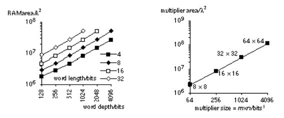
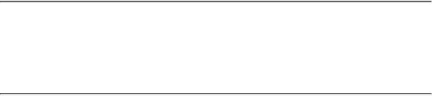
FIGURE 15.3 (a) ASIC memory size. These figures are for static RAM constructed using compilers in a 2LM ASIC process, but with no special memory design rules. The actual area of a RAM will depend on the speed and number of read write ports. (b) Multiplier size for a 2LM process. The actual area will depend on the multiplier architecture and speed.
The maximum size of SRAM in Figure 15.3 (a) is 32 k-bit, which occupies approximately 6.0 ¥ 10 7 l 2 . In a 0.5 m m process (with l = 0.25 m m), the area of a 32 k-bit SRAM is 6.0 ¥ 10 7 ¥ 0.25 ¥ 0.25 = 3.75 ¥ 10 6 m m 2 (or about 2 mm on a side a large piece of silicon). If you need an SRAM that is larger than this, you probably need to consult with your ASIC vendor to determine the best way to implement a large on-chip memory. Figure 15.3 (b) shows the typical sizes for multipliers. Again the actual multiplier size will depend on the architecture (Booth encoding, Wallace tree, and so on), the process technology, and design rules. Table 15.5 shows some estimated gate counts for medium-size functions corresponding to some popular ASSP devices.
TABLE 15.5 |
Gate size estimates for popular ASSP functions. |
|
|
ASSP |
Function |
Gate estimate |
|
device |
|||
|
|
||
8251A |
Universal synchronous/asynchronous |
2900 |
|
receiver/transmitter (USART) |
|||
|
|
||
8253 |
Programmable interval timer |
5680 |
|
8255A |
Programmable peripheral interface |
784 1403 |
|
8259 |
Programmable interrupt controller |
2205 |
|
8237 |
Programmable DMA controller |
5100 |
|
8284 |
Clock generator/driver |
99 |
|
8288 |
Bus controller |
250 |
8254 |
Programmable interval timer |
3500 |
6845 |
CRT controller |
2843 |
87030 |
SCSI controller |
3600 |
87012 |
Ethernet controller |
3900 |
2901 |
4 bit ALU |
917 |
2902 |
Carry-lookahead ALU |
33 |
2904 |
Status and shift control |
500 |
2910 |
12bit microprogram controller |
1100 |
Source: Fujitsu channelless gate-array data book, AU and CG21 series.
1.2LM = two-level metal; 3LM = three-level metal.
2.Area estimates are for a two-level metal (2 LM) process. Areas for a three-level metal (3LM) process are approximately 0.75 to 1.0 times these figures.