

6.5 Clock Input
When we bring the clock signal onto a chip, we may need to adjust the logic level (clock signals are often driven by TTL drivers with a high current output capability) and then we need to distribute the clock signal around the chip as it is needed. FPGAs normally provide special clock buffers and clock networks. We need to minimize the clock delay (or latency), but we also need to minimize the clock skew.
6.5.1 Registered Inputs
Some FPGAs provide a flip-flop or latch that you can use as part of the I/O circuit (registered I/O). For other FPGAs you have to use a flip-flop or latch using the basic logic cell in the core. In either case the important parameter is the input setup time. We can measure the setup with respect to the clock signal at the flip-flop or the clock signal at the clock input pad. The difference between these two parameters is the clock delay.
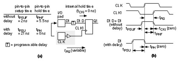
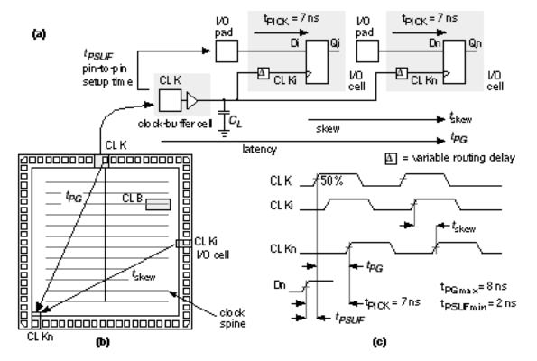
FIGURE 6.18 Clock input. (a) Timing model with values for a Xilinx XC4005-6. (b) A simplified view of clock distribution. (c) Timing diagram. Xilinx eliminates the variable internal delay t PG , by specifying a pin-to-pin setup time, t PSUFmin = 2 ns.
Figure 6.18 shows part of the I/O timing model for a Xilinx XC40005-6. 1
●t PICK is the fixed setup time for a flip-flop relative to the flip-flop clock.
●t skew is the variable clock skew , the signed delay between two clock edges.
●t PG is the variable clock delay or latency .
To calculate the flip-flop setup time ( t PSUFmin ) relative to the clock pad (which is the parameter system designers need to know), we subtract the clock delay, so that
t PSUF = t PICK t PG . (6.6)
The problem is that we cannot easily calculate t PG , since it depends on the clock distribution scheme and where the flip-flop is on the chip. Instead Xilinx specifies t PSUFmin directly, measured from the data pad to the clock pad; this time is called a pin-to-pin timing parameter . Notice t PSUF min = 2 ns ` t PICK t PG max = 1 ns.
Figure 6.19 shows that the hold time for a XC4005-6 flip-flop ( t CKI ) with respect to the flip-flop clock is zero. However, the pin-to-pin hold time including the clock delay is t PHF = 5.5 ns. We can remove this inconvenient hold-time restriction by delaying the input signal. Including a programmable delay allows Xilinx to guarantee the pin-to-pin hold time ( t PH ) as zero. The penalty is an
increase in the pin-to-pin setup time ( t PSU ) to 21 ns (from 2 ns) for the XC4005-6, for example.
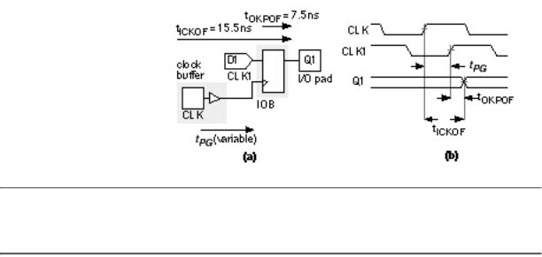
FIGURE 6.19 Programmable input delay. (a) Pin-to-pin timing model with values from an XC4005-6. (b) Timing diagrams with and without programmable delay.
We also have to account for clock delay when we register an output. Figure 6.20 shows the timing model diagram for the clock-to-output delay.
FIGURE 6.20
Registered output.
(a)Timing model with values for an XC4005-6 programmed with the fast slew-rate option.
(b)Timing diagram.
1.The Xilinx XC4005-6 timing parameters are from the 1994 data book p. 2-50 to p. 2-53.
6.6 Power Input
The last item that we need to bring onto an FPGA is the power. We may need multiple VDD and GND power pads to reduce supply bounce or separate VDD pads for mixed-voltage supplies. We may also need to provide power for on-chip programming (in the case of antifuse or EPROM programming technology). The package type and number of pins will determine the number of power pins, which, in turn, affects the number of SSOs you can have in a design.
6.6.1 Power Dissipation
As a general rule a plastic package can dissipate about 1 W, and more expensive ceramic packages can dissipate up to about 2 W. Table 6.3 shows the thermal characteristics of common packages. In a high-speed (high-power) design the ASIC power consumption may dictate your choice of packages. Actel provides a formula for calculating typical dynamic chip power consumption of their FPGAs. The formula for the ACT 2 and ACT 3 FPGAs are complex; therefore we shall use the simpler formula for the ACT 1 FPGAs as an example 1 :
TABLE 6.3 Thermal characteristics of ASIC packages.
q JA /°CW 1 q JA /°CW 1
Package 2 Pin count Max. power P max /W
|
|
|
(still air) 3 , |
4 |
(still air) 5 |
|
|
|
|
||
CPGA |
84 |
|
33 |
|
32 38 |
CPGA |
100 |
|
35 |
|
|
CPGA |
132 |
|
30 |
|
|
CPGA |
175 |
|
25 |
16 |
|
CPGA |
207 |
|
22 |
|
|
CPGA |
257 |
|
15 |
|
|
CQFP |
84 |
|
40 |
|
|
CQFP |
172 |
|
25 |
|
|
PQFP |
100 |
1.0 |
55 |
|
56 75 |
PQFP |
160 |
1.75 |
33 |
|
30 33 |
PQFP |
208 |
2.0 |
33 |
27-32 |
|
VQFP |
80 |
|
68 |
|
|
PLCC |
44 |
|
52 |
44 |
|
PLCC |
68 |
|
45 |
|
28 35 |

PLCC |
84 |
1.5 |
44 |
PPGA |
132 |
|
33 34 |
Total chip power = 0.2 (N ¥ F1) + 0.085 (M ¥ F2) + 0.8 ( P ¥ F3) mW (6.7)
where
F1 = average logic module switching rate in MHz
F2 = average clock pin switching rate in MHz
F3 = average I/O switching rate in MHz
M = number of logic modules connected to the clock pin
N = number of logic modules used on the chip
P = number of I/O pairs used (input + output), with 50 pF load
As an example of a power-dissipation calculation, consider an Actel 1020B-2 with a 20 MHz clock. We shall initially assume 100 percent utilization of the 547 Logic Modules and assume that each switches at an average speed of 5 MHz. We shall also initially assume that we use all of the 69 I/O Modules and that each switches at an average speed of 5 MHz. Using Eq. 6.7 , the Logic Modules dissipate
P LM = (0.2)(547)(5) = 547 mW , (6.8)
and the I/O Module dissipation is
P IO = (0.8)(69)(5) = 276 mW . (6.9)
If we assume the clock buffer drives 20 percent of the Logic Modules, then the additional power dissipation due to the clock buffer is
P CLK = (0.085)(547)(0.2)(5) = 46.495 mW . (6.10)
The total power dissipation is thus
P D = (547 + 276 + 46.5) = 869.5 mW , (6.11)
or about 900 mW (with an accuracy of certainly no better than ± 100 mW).
Suppose we intend to use a very thin quad flatpack ( VQFP ) with no cooling (because we are trying to save area and board height). From Table 6.3 the thermal
resistance, q JA , is approximately 68 °CW 1 for an 80-pin VQFP. Thus the maximum junction temperature under industrial worst-case conditions (T A = 85 °C) will be
T J = (85 + (0.87)(68)) = 144.16 °C , (6.12)

(with an accuracy of no better than 10 °C). Actel specifies the maximum junction temperature for its devices as T Jmax = 150 °C (T Jmax for Altera is also 150 °C, for Xilinx T Jmax = 125°C). Our calculated value is much too close to the rated maximum for comfort; therefore we need to go back and check our assumptions for power dissipation. At or near 100 percent module utilization is not unreasonable for an Actel device, but more questionable is that all nodes and I/Os switch at 5 MHz.
Our real mistake is trying to use a VQFP package with a high q JA for a high-speed design. Suppose we use an 84-pin PLCC package instead. From Table 6.3 the thermal resistance, q JA , for this alternative package is
approximately 44 °CW 1 . Now the worst-case junction temperature will be a more reasonable
T J = (85 + (0.87)(44)) = 123.28 °C , (6.13)
It is possible to estimate the power dissipation of the Actel architecture because the routing is regular and the interconnect capacitance is well controlled (it has to be since we must minimize the number of series antifuses we use). For most other architectures it is much more difficult to estimate power dissipation. The exception, as we saw in Section 5.4 Altera MAX, are the programmable ASICs based on programmable logic arrays with passive pull-ups where a substantial part of the power dissipation is static.
6.6.2 Power-On Reset
Each FPGA has its own power-on reset sequence. For example, a Xilinx FPGA configures all flip-flops (in either the CLBs or IOBs) as either SET or RESET. After chip programming is complete, the global SET/RESET signal forces all flip-flops on the chip to a known state. This is important since it may determine the initial state of a state machine, for example.
1.1994 data book, p.1-9
2.CPGA = ceramic pin-grid array; CQFP = ceramic quad flatpack; PQFP = plastic quad flatpack; VQFP = very thin quad flatpack; PLCC = plastic leaded chip carrier; PPGA = plastic pin-grid array.
3.q JA varies with die size.
4.Data from Actel 1994 data book p. 1-9, p. 1-45, and p. 1-94.
5.Data from Xilinx 1994 data book p. 4-26 and p. 4-27.