

8.2 Logic Synthesis
Designers are increasingly using logic synthesis as a replacement for schematic entry. As microelectronic systems and their ASICs become more complex, the use of schematics becomes less practical. For example, a complex ASIC that contains over 10,000 gates might require hundreds of pages of schematics at the gate level. As another example, it is easier to write A = B + C than to draw a schematic for a 32-bit adder at the gate level.
The term logic synthesis is used to cover a broad range of software and software capabilities. Many logic synthesizers are based on logic minimization. Logic minimization is usually performed in one of two ways, either using a set of rules or using algorithms. Early logic-minimization software was designed using algorithms for two-level logic minimization and developed into multilevel logic-optimization software. Two-level and multilevel logic minimization is well suited to random logic that is to be implemented using a CBIC, MGA, or PLD. In these technologies, two-level logic can be implemented very efficiently. Logic minimization for FPGAs, including complex PLDs, is more difficult than other types of ASICs, because of the complex basic logic cells in FPGAs.
There are two ways to use logic synthesis in the design of FPGAs. The first and simplest method takes a hardware description, optimizes the logic, and then produces a netlist. The netlist is then passed to software that maps the netlist to an FPGA architecture. The disadvantage of this method is the inefficiency of decoupling the logic optimization from the mapping step. The second, more complicated, but more efficient method, takes the hardware description and directly optimizes the logic for a specific FPGA architecture.
Some logic synthesizers produce files in PALASM, ABEL, or CUPL formats. Software provided by the FPGA vendor then take these files and maps the logic to the FPGA architecture. The FPGA mapping software requires detailed knowledge of the FPGA architecture. This makes it difficult for third-party companies to create logic synthesis software that can map directly to the FPGA.
A problem with design-entry systems is the difficulty of moving netlists between different FPGA vendors. Once you have completed a design using an FPGA cell library, for example, you are committed to using that type of FPGA unless you repeat design entry using a different cell library. ASIC designers do not like this approach since it exposes them to the mercy of a single ASIC vendor. Logic synthesizers offer a degree of independence from FPGA vendors (universally referred to vendor independence, but this should, perhaps, be designer
independence) by delaying the point in the design cycle at which designers need to make a decision on which FPGA to use. Of course, now designers become dependent on the synthesis software company.
8.2.1 FPGA Synthesis
For low-level logic synthesis, PALASM is a de facto standard as the lowest-common-denominator interchange format. Most FPGA design systems are capable of converting their own native formats into a PALASM file. The most common programmable logic design systems are ABEL from Data I/O, CUPL from P-CAD, LOG/iC from IsData, PALASM2 from AMD, and PGA-Designer from Minc. At a higher level, CAD companies (Cadence, Compass, Mentor, and Synopsys are examples) support most FPGA cell libraries. This allows you to map from a VHDL or Verilog description to an EDIF netlist that is compatible with FPGA design software. Sometimes you have to buy the cell library from the software company, sometimes from the FPGA vendor.
TABLE 8.3 The VHDL code for the sequence detector of Table 8.2 .
entity detector is port (X, CLK: in BIT; Z : out BIT); end;
architecture behave of SEQDET is
type STATES is (S1, S2, S3, S4);
signal current, next: STATES;
begin
combinational: process begin
case current is
when S1 =>
if X = '1' then Z <= '0'; next <= S3; else Z <= '0'; next <= S1; end if;
when S2 =>
if X = '1' then Z <= '0'; next <= S2; else Z <= '0'; next <= S1; end if;
when S3 =>
if X = '1' then Z <= '0'; next <= S2; else Z <= '0'; next <= S1; end if;
when S4 =>
if X = '1' then Z <= '1'; next <= S4; else Z <= '0'; next <= S1; end if
end case;
end process

sequential: process begin
wait until CLK'event and CLK = '1'; current <= next ;
end process;
end behave;
As an example, Table 8.3 shows a VHDL model for a pattern detector to check for a sequence of three '1's (excluding the code for the I/O pads). Table 8.4 shows a script or command file that runs the Synopsys software to generate an EDIF netlist from this VHDL that targets the TI version of the Actel FPGA parts. A script is a recipe that tells the software what to do. If we wanted to retarget this design to another type of FPGA or an MGA or CBIC ASIC, for example, we may only need a new set of cell libraries and to change the script (if we are lucky). In practice, we shall probably find we need to make a few changes in the VHDL code (in the areas of I/O pads, for example, that are different for each kind of ASIC). We now have a portable design and a measure of vendor independence. We have also introduced some dependence on the Synopsys software since the code in Table 8.3 might be portable, but the script (which is just as important a part of the design) in Table 8.4 may only be used with the Synopsys software. Nevertheless, using logic synthesis results in a more portable design than using schematic entry.
TABLE 8.4 The Synopsys script for the VHDL code of Table 8.3 .
/design checking/ |
report_design > detector.rpt |
search_path = . |
/optimize for area/ |
/use the TI cell libraries/ |
max_area 0.0 |
link_library = tpc10.db |
compile |
target_library = tpc10.db |
write -h -f db -o detector_opt.db |
symbol_library = tpc10.sdb |
report -area -cell -timing > detector.rpt |
read -f vhdl detector.vhd |
free -all |
current_design = detector |
/write EDIF netlist/ |
write -n -f db -hierarchy -0 detector.db write -h -f edif -0 |
|
check_design > detector.rpt |
exit |
8.3 The Halfgate ASIC
This section illustrates FPGA design using a very simple ASIC a single inverter. The hidden details of the design and construction of this halfgate FPGA are quite complicated. Fortunately, most of the inner workings of the design software are normally hidden from the designer. However, when software breaks, as it sometimes does, it is important to know how things work in order to fix the problem. The formats, filenames, and flow will change, but the information needed at each stage and the order in which it is conveyed will stay much the same.
8.3.1 Xilinx
Table 8.5 shows an FPGA design flow using Compass and Xilinx software. On the left of Table 8.5 is a script for the Compass programs scripts for Cadence, Mentor, and Synopsys software are similar, but not all design software has the capability to be run on autopilot using scripts and a command language. The diagrams in Table 8.5 illustrate what is happening at each of the design steps. The following numbered comments, corresponding to the labels in Table 8.5 , highlight the important steps:
TABLE 8.5 Design flow for the Xilinx implementation of the halfgate ASIC.
Script |
Design flow |
#
halfgate.xilinx.inp
shell setdef
path working xc4000d xblox cmosch000x
quit
asic
open [v]halfgate
synthesize
save [nls]halfgate_p
quit
fpga
set tag xc4000
set opt area
optimize [nls]halfgate_p
quit
qtv
open [nls]halfgate_p
trace critical
print trace [txt]halfgate_p
quit

shell vuterm
exec xnfmerge -p 4003PC84 halfgate_p > /dev/null
exec xnfprep halfgate_p > /dev/null
exec ppr halfgate_p > /dev/null
exec makebits -w halfgate_p > /dev/null
exec lca2xnf -g -v halfgate_p halfgate_b > /dev/null
quit
manager notice
utility netlist
open [xnf]halfgate_b
save [nls]halfgate_b
save [edf]halfgate_b
quit
qtv
open [nls]halfgate_b
trace critical
print trace [txt]halfgate_b
quit
TABLE 8.6 The Xilinx files for the halfgate ASIC. Verilog file (halfgate.v)

Preroute XNF file (halfgate_p.xnf)
LCA file (halfgate_p.lca)
Postroute XNF file (halfgate_b.xnf)
1.The Verilog code, in halfgate.v , describes a single inverter.
2.The script runs the logic synthesizer that converts the Verilog description to an inverter (using elements from the Xilinx XC4000 library) and saves the result in a netlist, halfgate_p.nls (a Compass internal format).
3.The script next runs the logic optimizer for FPGAs. This program also adds the I/O pads. In this case, logic optimization implements the inverter by using an inverting output pad. The software writes out the netlist as halfgate_p.xnf .
4.A timing simulation is run on the netlist halfgate_p.nls (the Compass format netlist). This netlist uses the default delays every gate has a delay of 1 ns.
5.At this point the script has run all of the Xilinx programs required to complete the place-and-route step. The Xilinx programs have created several files, the most important of which is halfgate_p.lca , which describes the FPGA layout. This postroute netlist is converted to halfgate_b.nls (the added suffix 'b' stands for back-annotation). Next a timing simulation is performed on the postroute netlist, which now includes delays, to find the delay from the input ( myInput ) to the output ( myOutput ). This is the critical and onlypath. The simulation (not shown) reveals that the delay is 2.8 ns (for the input buffer) plus 11.6 ns (for the output buffer), for a total delay of 14.4 ns (this is for a XC4003 in a PC84 package, and default speed grade '4').
Table 8.6 shows the key Xilinx files that are created. The preroute file, halfgate_p.xnf , describes the IBUF and OBUF library cells but does not contain any delays. The LCA file, halfgate_p.lca , contains all the physical design information, including the locations of the pads and I/O cells on the FPGA ( PAD61 for myInput and PAD1 for myOutput ), as well as the details of the programmable connections between these I/O Cells. The postroute file, halfgate_b.xnf , is similar to the preroute version except that now the delays are included. Xilinx assigns delays to a pin (connector or terminal of a cell). In this case 2.8 ns is assigned to the output of the input buffer, 8.6 ns is assigned to the input of the output buffer, and finally 3.0 ns is assigned to the output of the output buffer.
8.3.2 Actel
The key Actel files for the halfgate design are the netlist file, halfgate_io.adl, and the STF delay file for back-annotation, halfgate_io.stf. Both of these files are shown in Table 8.7 (the STF file is large and only the last few lines, which contain the delay information, are shown in the table).
TABLE 8.7 The Actel files for the halfgate ASIC.
ADL file |
STF file |
;HEADER
;FILEID STF ./halfgate_io.stf c96ef4d8
... lines omitted ... (126 lines total)
;HEADER
;FILEID ADL ./halfgate_io.adl 85e8053b
DEF halfgate_io.
; CHECKSUM 85e8053b
USE ; INBUF_2/U0;
; PROGRAM certify
TPADH:'11:26:37',
; VERSION 23/1
TPADL:'13:30:41',
; ALSMAJORREV 2
TPADE:'12:29:41',
; ALSMINORREV 3
TPADD:'20:48:70',
; ALSPATCHREV .1
TYH:'8:20:27',
; NODEID 72705192
TYL:'12:28:39'.
; VAR FAMILY 1400
PIN u2:A;
; ENDHEADER
RDEL:'13:31:42',
DEF halfgate_io; myInput, myOutput.
FDEL:'11:26:37'.
USE ADLIB:INBUF; INBUF_2.
USE ; OUTBUF_3/U0;
USE ADLIB:OUTBUF; OUTBUF_3.
TPADH:'11:26:37',
USE ADLIB:INV; u2.
TPADL:'13:30:41',
NET DEF_NET_8; u2:A, INBUF_2:Y.
TPADE:'12:29:41',
NET DEF_NET_9; myInput, INBUF_2:PAD.
TPADD:'20:48:70',
NET DEF_NET_11; OUTBUF_3:D, u2:Y.
TYH:'8:20:27',
NET DEF_NET_12; myOutput, OUTBUF_3:PAD.
TYL:'12:28:39'.
END.
PIN OUTBUF_3/U0:D;
RDEL:'14:32:45',
FDEL:'11:26:37'.
END.
8.3.3 Altera
Because Altera complex PLDs use a deterministic routing structure, they can be designed more easily using a self-contained software package an all-in-one software package using a single interface. We shall assume that we can generate a netlist that the Altera software can accept using Cadence, Mentor, or Compass software with an Altera design kit (the most convenient format is EDIF).
Table 8.8 shows the EDIF preroute netlist in a format that the Altera software can accept. This netlist file describes a single inverter (the line 'cellRef not'). The majority of the EDIF code in Table 8.8 is a standard template to pass information about how the VDD and VSS nodes are named, which libraries are used, the name of the design, and so on. We shall cover EDIF in Chapter 9 .
TABLE 8.8 EDIF netlist in Altera format for the halfgate ASIC.
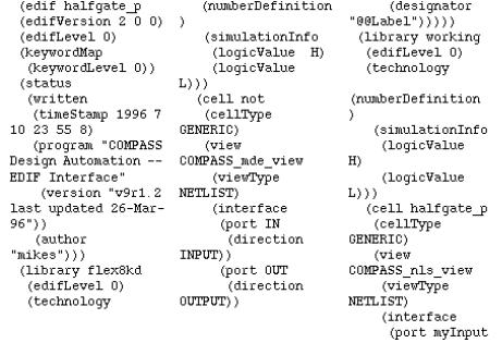
Table 8.9 shows a small part of the reports generated by the Altera software after completion of the place-and-route step. This report tells us how the software has used the basic logic cells, interconnect, and I/O cells to implement our design. With practice it is possible to read the information from reports such as Table 8.9 directly, but it is a little easier if we also look at the netlist. The EDIF version of postroute netlist for this example is large. Fortunately, the Altera software can also generate a Verilog version of the postroute netlist. Here is the generated Verilog postroute netlist, halfgate_p.vo (not '.v' ), for the halfgate design:
TABLE 8.9 Report for the halfgate ASIC fitted to an Altera MAX 7000 complex PLD. ** INPUTS **
Shareable
Expanders Fan-In Fan-Out
Pin LC LAB Primitive Code Total Shared n/a INP FBK OUT FBK Name
43 - - INPUT 0 0 0 0 0 0 1 myInput ** OUTPUTS **
Shareable
Expanders Fan-In Fan-Out
Pin LC LAB Primitive Code Total Shared n/a INP FBK OUT FBK Name
41 17 B OUTPUT t 0 0 0 1 0 0 0 myOutput ** LOGIC CELL INTERCONNECTIONS **
Logic Array Block 'B':
+- LC17 myOutput
|
LC | | A B | Name
Pin
43 -> * | - * | myInput
* = The logic cell or pin is an input to the logic cell (or LAB) through the PIA.
- = The logic cell or pin is not an input to the logic cell (or LAB).
//halfgate_p (EPM7032LC44) MAX+plus II Version 5.1 RC6 10/03/94
//Wed Jul 17 04:07:10 1996
`timescale 100 ps / 100 ps
module TRI_halfgate_p( IN, OE, OUT ); input IN; input OE; output OUT;
bufif1 ( OUT, IN, OE );
specify
specparam TTRI = 40; specparam TTXZ = 60; specparam TTZX = 60;
(IN => OUT) = (TTRI,TTRI);
(OE => OUT) = (0,0, TTXZ, TTZX, TTXZ, TTZX);
endspecify
endmodule
module halfgate_p (myInput, myOutput);
input myInput; output myOutput; supply0 gnd; supply1 vcc;
wire B1_i1, myInput, myOutput, N_8, N_10, N_11, N_12, N_14;
TRI_halfgate_p tri_2 ( .OUT(myOutput), .IN(N_8), .OE(vcc) );
TRANSPORT transport_3 ( N_8, N_8_A );
defparam transport_3.DELAY = 10;
and delay_3 ( N_8_A, B1_i1 );
xor xor2_4 ( B1_i1, N_10, N_14 );
or or1_5 ( N_10, N_11 );
TRANSPORT transport_6 ( N_11, N_11_A );
defparam transport_6.DELAY = 60;
and and1_6 ( N_11_A, N_12 );
TRANSPORT transport_7 ( N_12, N_12_A );
defparam transport_7.DELAY = 40;
not not_7 ( N_12_A, myInput );
TRANSPORT transport_8 ( N_14, N_14_A );
defparam transport_8.DELAY = 60;
and and1_8 ( N_14_A, gnd );
endmodule
The Verilog model for our ASIC, halfgate_p , is written in terms of other models: and , xor , or , not , TRI_halfgate_p , TRANSPORT . The first four of these are primitive models for basic logic cells and are built into the Verilog simulator. The model for TRI_halfgate_p is generated together with the rest of the code. We also need the following model for TRANSPORT, which contains the delay information for the Altera MAX complex PLD. This code is part of a file ( alt_max2.vo ) that is generated automatically.
// MAX+plus II Version 5.1 RC6 10/03/94 Wed Jul 17 04:07:10 1996
`timescale 100 ps / 100 ps
module TRANSPORT( OUT, IN ); input IN; output OUT; reg OUTR;
wire OUT = OUTR; parameter DELAY = 0;
`ifdef ZeroDelaySim
always @IN OUTR <= IN;
`else
always @IN OUTR <= #DELAY IN;
`endif
`ifdef Silos
initial #0 OUTR = IN;
`endif
endmodule
The Altera software can also write the following VHDL postroute netlist:
--halfgate_p (EPM7032LC44) MAX+plus II Version 5.1 RC6 10/03/94
--Wed Jul 17 04:07:10 1996
LIBRARY IEEE; USE IEEE.std_logic_1164.all;
ENTITY n_tri_halfgate_p IS
GENERIC (ttri: TIME := 1 ns; ttxz: TIME := 1 ns; ttzx: TIME := 1 ns); PORT (in0 : IN X01Z; oe : IN X01Z; out0: OUT X01Z);
END n_tri_halfgate_p;
ARCHITECTURE behavior OF n_tri_halfgate_p IS
BEGIN
PROCESS (in0, oe) BEGIN
IF oe'EVENT THEN
IF oe = '0' THEN out0 <= TRANSPORT 'Z' AFTER ttxz; ELSIF oe = '1' THEN out0 <= TRANSPORT in0 AFTER ttzx; END IF;
ELSIF oe = '1' THEN out0 <= TRANSPORT in0 AFTER ttri; END IF;
END PROCESS;
END behavior;
LIBRARY IEEE; USE IEEE.std_logic_1164.all; USE work.n_tri_halfgate_p; ENTITY n_halfgate_p IS
PORT ( myInput : IN X01Z; myOutput : OUT X01Z);
END n_halfgate_p;
ARCHITECTURE EPM7032LC44 OF n_halfgate_p IS
SIGNAL gnd : X01Z := '0'; SIGNAL vcc : X01Z := '1';
SIGNAL n_8, B1_i1, n_10, n_11, n_12, n_14 : X01Z;
COMPONENT n_tri_halfgate_p
GENERIC (ttri, ttxz, ttzx: TIME);
PORT (in0, oe : IN X01Z; out0 : OUT X01Z);
END COMPONENT;
BEGIN

PROCESS(myInput) BEGIN ASSERT myInput /= 'X' OR Now = 0 ns
REPORT "Unknown value on myInput" SEVERITY Warning;
END PROCESS;
n_tri_2: n_tri_halfgate_p
GENERIC MAP (ttri => 4 ns, ttxz => 6 ns, ttzx => 6 ns)
PORT MAP (in0 => n_8, oe => vcc, out0 => myOutput);
n_delay_3: n_8 <= TRANSPORT B1_i1 AFTER 1 ns;
n_xor_4: B1_i1 <= n_10 XOR n_14;
n_or_5: n_10 <= n_11;
n_and_6: n_11 <= TRANSPORT n_12 AFTER 6 ns;
n_not_7: n_12 <= TRANSPORT NOT myInput AFTER 4 ns;
n_and_8: n_14 <= TRANSPORT gnd AFTER 6 ns;
END EPM7032LC44;
LIBRARY IEEE; USE IEEE.std_logic_1164.all; USE work.n_halfgate_p;
ENTITY halfgate_p IS
PORT ( myInput : IN std_logic; myOutput : OUT std_logic);
END halfgate_p;
ARCHITECTURE EPM7032LC44 OF halfgate_p IS
COMPONENT n_halfgate_p PORT (myInput : IN X01Z; myOutput : OUT X01Z);
END COMPONENT;
BEGIN
n_0: n_halfgate_p
PORT MAP ( myInput => TO_X01Z(myInput), myOutput => myOutput);
END EPM7032LC44;
The VHDL is a little harder to decipher than the Verilog, so the schematic for the VHDL postroute netlist is shown in Figure 8.2 . This VHDL netlist is identical in function to the Verilog netlist, but the net names and component names are different. Compare Figure 8.2 with Figure 5.15 (c) in Section 5.4 , Altera MAX , which shows the Altera basic logic cell and Figure 6.23 in Section 6.8, Other I/O Cells, which describes the Altera I/O cell. The software has fixed the inputs to the various elements in the Altera MAX device to implement a single inverter.
FIGURE 8.2 The VHDL version of the postroute Altera MAX 7000 schematic for the halfgate ASIC. Compare this with Figure 5.15(c) and Figure 6.23.