


15.8 Summary
The construction or physical design of ASICs in a microelectronics system is a very large and complex problem. To solve the problem we divide it into several steps: system partitioning, floorplanning, placement, and routing. To solve each of these smaller problems we need goals and objectives, measurement metrics, as well as algorithms and methods.
System partitioning is the first step in ASIC assembly. An example of the SPARCstation 1 illustrated the various issues involved in partitioning. Presently commercial CAD tools are able to automatically partition systems and chips only at a low level, at the level of a network or netlist. Partitioning for FPGAs is currently the most advanced. Next we discussed the methods to use for system partitioning. We saw how to represent networks as graphs, containing nets and edges, and how the mathematics of graph theory is useful in system partitioning and the other steps of ASIC assembly. We covered methods and algorithms for partitioning and explained that most are based on the Kernighan Lin min-cut algorithm.
The important points in this chapter are
●The goals and objectives of partitioning
●Partitioning as an art not a science
●The simple nature of the algorithms necessary for VLSI-sized problems
●The random nature of the algorithms we use
●The controls for the algorithms used in ASIC design
15.10 Bibliography
Many of the references in the bibliography in Chapter 1 are also sources for information on the physical design of ASICs. The European Conference on Design Automation is known as EuroDAC (TK7867.E93, ISBN and cataloging varies with year). Another European conference, EuroASIC, was absorbed by EuroDAC (TK7874.6.E88, ISSN 1066-1409 and ISSN 1064-5322, cataloging varies).
Preas and Lorenzetti s book [ 1988] contains an overview chapter on partitioning and placement. To dig a little deeper see the review article by Goto and Matsud [1986]. If you want to explore further the detailed workings of partitioning algorithms, Sherwani s book [ 1993] catalogs physical design algorithms, including those for partitioning. To learn more about simulated annealing see Sechen s book [ 1988]. Partitioning is an important part of high-level synthesis, and the book by Gajski et al. [ 1992] contains a chapter on partitioning for allocation and scheduling as well as system partitioning including a description of clustering methods, which are not well covered elsewhere.This book describes SpecSyn, a tool that allows you to enter a design using a behavioral description with a graphical tool. SpecSyn can then partition the design given area, timing, and cost specifications. System partitioning at the behavioral level ( architectural partitioning) is an area of current research (see [ Lagnese and Thomas, 1991] for a description of the APARTY system). This means we partition a design based on a hardware design language rather than a schematic or other physical description. Papers published in the Proceedings of the Design Automation Conference (DAC) and articles in the IEEE Transactions on Computer-Aided Design of Integrated Circuits and Systems form a point at which to start working back through the recent research literature on system partitioning, an example is [ Kucukcakar and Parker, 1991].
The Proceedings of the 32nd Design Automation Conference (1995) describe a special session on the design of the Sun Microsystems UltraSPARC-I (albeit from more of a systems perspective), which forms an interesting comparison to the SPARCstation 1 and SPARCstation 10 designs.
15.11 References
Page numbers in brackets after the reference indicate the location in the chapter body.
Cheng, C.-K., and Y.-C. A. Wei. 1991. An improved two-way partitioning algorithm with stable performance. IEEE Transactions on Computer-Aided Design of Integrated Circuits and Systems, Vol. 10, no. 12, pp. 1502 1511.
Describes the ratio-cut algorithm. [ reference location ]
Fiduccia, C. M., and R. M. Mattheyses. 1982. A linear-time heuristic for improving network partitions. In Proceedings of the 19th Design Automation Conference, pp. 175 181. Describes modification to Kernighan-Lin algorithm to reduce computation time. [ reference location ]
Gajski, D. D., N. D. Dutt, A. C.-H. Wu, and S. Y.-L. Lin. 1992. High-Level Synthesis: Introduction to Chip and System Design. Norwell, MA: Kluwer. ISBN 0-7923-9194-2. TK7874.H52422. Chapter 6, Partitioning, is an introduction to system-level partitioning algorithms. It also includes a description of the system partitioning features of SpecSyn, a research tool developed at UC-Irvine. [ reference location ]
Goto, S., and T. Matsud. 1986. Partitioning, assignment and placement. In Layout Design and Verification. Vol. 4 of Advances in CAD for VLSI (T. Ohtsuki, Ed.) pp. 55 97, New York: Elsevier. [ reference location ]
Kernighan, B. W., and S. Lin. 1970. An efficient heuristic procedure for partitioning graphs. Bell Systems Technical Journal, Vol. 49, no. 2, February, pp. 291 307. The original description of the Kernighan Lin partitioning algorithm. [ reference location ]
Kirkpatrick, S., et al. 1983. Optimization by simulated annealing. Science, Vol. 220, no. 4598, pp. 671 680. [ reference location ]
Kucukcakar, K., and A. C. Parker, 1991. CHOP: A constraint-driven system-level partitioner. In Proceedings of the 28th Design Automation Conference, pp. 514 519. [ reference location ]
Lagnese, E., and D. Thomas. 1991. Architectural partitioning for system level synthesis of integrated circuits. IEEE Transactions on Computer-Aided Design of Integrated Circuits and Systems, Vol. 10, no. 7, pp. 847 860. [ reference location ]

Najm, F. N. 1994. A survey of power estimation techniques in VLSI circuits. IEEE Transactions on Very Large Scale Integration (VLSI) Systems, Vol. 2, no. 4, pp. 446 455. 43 refs. [ reference location ]
Preas, B. T., and P. G. Karger, 1988. Placement, assignment and floorplanning. In Physical Design Automation of VLSI Systems (B. T. Preas and M. J. Lorenzetti, Eds.), pp. 87 155. Menlo Park, CA: Benjamin-Cummings. ISBN 0-8053-0412-9. TK7874.P47. [ reference location ]
Rose, J., W. Klebsch, and J. Wolf, 1990. Temperature measurement and equilibrium dynamics of simulated annealing placements. IEEE Transactions on Computer-Aided Design of Integrated Circuits and Systems, Vol. 9, no. 3, pp. 253 259. Discusses ways to speed up simulated annealing. [ reference location ]
Schweikert, D. G., and B. W. Kernighan. 1979. A proper model for the partitioning of electrical circuits. In Proceedings of the 9th Design Automation Workshop. Points out the difference between nets and edges. [ reference location , reference location ]
Sechen, C. 1988. VLSI Placement and Global Routing Using Simulated Annealing. New York: Kluwer. Introduction; The Simulated Annealing Algorithm; Placement and Global Routing of Standard Cell Integrated Circuits; Macro/Custom Cell Chip-Planning, Placement, and Global Routing; Average Interconnection Length Estimation; Interconnect-Area Estimation for Macro Cell Placements; An Edge-Based Channel Definition Algorithm for Rectilinear Cells; A Graph-Based Global Router Algorithm; Conclusion; Island-Style Gate Array Placement. [ reference location ]
Sedgewick, R. 1988. Algorithms. Reading, MA: Addison-Wesley. ISBN 0-201-06673-4. QA76.6.S435. Reference for basic sorting and graph-searching algorithms. [ reference location ]
Sherwani, N. A. 1993. Algorithms for VLSI Physical Design Automation. Norwell, MA: Kluwer. ISBN 0-7923-9294-9. TK874.S455. [ reference location ]
Smailagic, A., et al. 1995. Benchmarking an interdisciplinary concurrent design methodology for electronic/mechanical systems. In Proceedings of the 32nd Design Automation Conference. San Francisco. Describes the evolution of the VuMan wearable computer. Includes some interesting measures of the complexity of system design. [ reference location ]
Veendrick, H. J. M. 1984. Short-circuit dissipation of static CMOS circuitry and its impact on the design of buffer circuits. IEEE Journal of Solid-State Circuits, Vol. SC-19, no. 4, pp. 468 473. [ reference location , reference location ]
Last Edited by SP 14112004
FLOORPLANNING
AND
PLACEMENT
The input to the floorplanning step is the output of system partitioning and design entry a netlist. Floorplanning precedes placement, but we shall cover them together. The output of the placement step is a set of directions for the routing tools.
At the start of floorplanning we have a netlist describing circuit blocks, the logic cells within the blocks, and their connections. For example, Figure 16.1 shows the Viterbi decoder example as a collection of standard cells with no room set aside yet for routing. We can think of the standard cells as a hod of bricks to be made into a wall. What we have to do now is set aside spaces (we call these spaces the channels ) for interconnect, the mortar, and arrange the cells.
Figure 16.2 shows a finished wall after floorplanning and placement steps are complete. We still have not completed any routing at this point that comes laterall we have done is placed the logic cells in a fashion that we hope will minimize the total interconnect length, for example.

FIGURE 16.1 The starting point for the floorplanning and placement steps for the Viterbi decoder (containing only standard cells). This is the initial display of the floorplanning and placement tool. The small boxes that look like bricks are the outlines of the standard cells. The largest standard cells, at the bottom of the display (labeled dfctnb) are 188 D flip-flops. The '+' symbols represent the drawing origins of the standard cells for the D flip-flops they are shifted to the left and below the logic cell bottom left-hand corner. The large box surrounding all the logic cells represents the estimated chip size. (This is a screen shot from Cadence Cell Ensemble.)
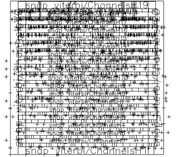
FIGURE 16.2 The Viterbi Decoder (from Figure 16.1 ) after floorplanning and placement. There are 18 rows of standard cells separated by 17 horizontal channels (labeled 2 18). The channels are routed as numbered. In this example, the I/O pads are omitted to show the cell placement more clearly. Figure 17.1 shows the same placement without the channel labels. (A screen shot from Cadence Cell Ensemble.)