

3.7 Standard-Cell Design
Figure 3.19 shows the components of the standard cell from Figure 1.3. Each
standard cell in a library is rectangular with the same height but different widths. The bounding box ( BB ) of a logic cell is the smallest rectangle that encloses all of the geometry of the cell. The cell BB is normally determined by the well layers. Cell connectors or terminals (the logical connectors ) must be placed on the cell abutment box ( AB ). The physical connector (the piece of metal to which we connect wires) must normally overlap the abutment box slightly, usually by at least 1 l , to assure connection without leaving a tiny space between the ends of two wires. The standard cells are constructed so they can all be placed next to each other horizontally with the cell ABs touching (we abut two cells).
(a) |
(b) |
(c) |
(d) |
|
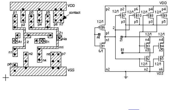
FIGURE 3.19 (a) The standard cell shown in Figure 1.3. (b) Diffusion, poly, and contact layers. (c) m1 and contact layers. (d) The equivalent schematic.
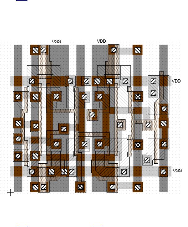
A standard cell (a D flip-flop with clear) is shown in Figure 3.20 and illustrates the following features of standard-cell layout:
●Layout using 45° angles. This can save 10% 20% in area compared to a cell that uses only Manhattan or 90° geometry. Some ASIC vendors do not allow transistors with 45° angles; others do not allow 45° angles at all.
●Connectors are at the top and bottom of the cell on m2 on a routing grid equal to the vertical (m2) track spacing. This is a double-entry cell intended for a two-level metal process. A standard cell designed for a three-level metal process has connectors in the center of the cell.
●Transistor sizes vary to optimize the area and performance but maintain a fixed ratio to balance rise times and fall times.
●The cell height is 64 l (all cells in the library are the same height) with a horizontal (m1) track spacing of 8 l . This is close to the minimum height that can accommodate the most complex cells in a library.
●The power rails are placed at the top and bottom, maintaining a certain width inside the cell and abut with the power rails in adjacent cells.
●The well contacts (substrate connections) are placed inside the cell at regular intervals. Additional well contacts may be placed in spacers between cells.
●In this case both wells are drawn. Some libraries minimize the well or moat area to reduce leakage and parasitic capacitance.
●Most commercial standard cells use m1 for the power rails, m1 for internal connections, and avoid using m2 where possible except for cell connectors.
FIGURE 3.20 A D flip-flop standard cell. The wide power buses and transistors show this is a performance-optimized cell. This double-entry cell is intended for a two-level metal process and channel routing. The five connectors run vertically through the cell on m2 (the extra short vertical metal line is an internal crossover).
When a library developer creates a gate-array, standard-cell, or datapath library, there is a trade-off between using wide, high-drive transistors that result in large cells with high-speed performance and using smaller transistors that result in smaller cells that consume less power. A performance-optimized library with large cells might be used for ASICs in a high-performance workstation, for example. An area-optimized library might be used in an ASIC for a battery-powered portable computer.
3.8 Datapath-Cell Design
Figure 3.21 shows a datapath flip-flop. The primary, thicker, power buses run
vertically on m2 with thinner, internal power running horizontally on m1. The control signals (clock in this case) run vertically through the cell on m2. The control signals that are common to the cells above and below are connected directly in m2. The other signals (data, q, and qbar in this example) are brought out to the wiring channel between the rows of datapath cells.
FIGURE 3.21 A datapath D flip-flop cell.
Figure 3.22 is the schematic for Figure 3.21 . This flip-flop uses a pair of
cross-coupled inverters for storage in both the master and slave latches. This leads to a smaller and potentially faster layout than the flip-flop circuits that we
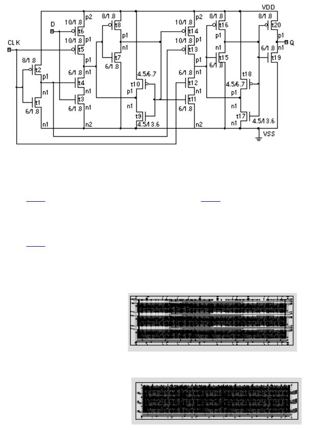
use in gate-array and standard-cell ASIC libraries. The device sizes of the inverters in the data-path flip-flops are adjusted so that the state of the latches may be changed. Normally using this type of circuit is dangerous in an uncontrolled environment. However, because the datapath structure is regular and known, the parasitic capacitances that affect the operation of the logic cell are also known. This is another advantage of the datapath structure.
FIGURE 3.22 The schematic of the datapath D flip-flop cell shown in Figure 3.21 .
Figure 3.23 shows an example of a datapath. Figure 3.23 (a) depicts a two-level
metal version showing the space between rows or slices of the datapath. In this case there are many connections to be brought out to the right of the datapath, and this causes the routing channel to be larger than normal and thus easily seen. Figure 3.23 (b) shows a three-level metal version of the same datapath. In this
case more of the routing is completed over the top of the datapath slices, reducing the size of the routing channel.
FIGURE 3.23 A datapath. (a) Implemented in a two-level metal process. (b) Implemented in a three-level metal process.
(a)
(b)