

5.2 Xilinx LCA
Xilinx LCA (a trademark, denoting logic cell array) basic logic cells, configurable logic blocks or CLBs , are bigger and more complex than the Actel or QuickLogic cells. The Xilinx LCA basic logic cell is an example of a coarse-grain architecture . The Xilinx CLBs contain both combinational logic and flip-flops.
5.2.1 XC3000 CLB
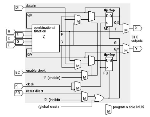
The XC3000 CLB, shown in Figure 5.6 , has five logic inputs (A E), a common clock input (K), an asynchronous direct-reset input (RD), and an enable (EC). Using programmable MUXes connected to the SRAM programming cells, you can independently connect each of the two CLB outputs (X and Y) to the output of the flip-flops (QX and QY) or to the output of the combinational logic (F and G).
FIGURE 5.6 The Xilinx XC3000 CLB (configurable logic block). (Source: Xilinx.)
A 32-bit look-up table ( LUT ), stored in 32 bits of SRAM, provides the ability to implement combinational logic. Suppose you need to implement the function F = A · B · C · D · E (a five-input AND). You set the contents of LUT cell number 31 (with address '11111') in the 32-bit SRAM to a '1'; all the other SRAM cells are set to '0'. When you apply the input variables as an address to the 32-bit SRAM, only when ABCDE = '11111' will the output F be a '1'. This means that the CLB propagation delay is fixed, equal to the LUT access time, and independent of the logic function you implement.
There are seven inputs for the combinational logic in the XC3000 CLB: the five CLB inputs (A E), and the flip-flop outputs (QX and QY). There are two outputs from the LUT (F and G). Since a 32-bit LUT requires only five variables to form a unique address (32 = 2 5 ), there are several ways to use the LUT:
●You can use five of the seven possible inputs (A E, QX, QY) with the entire 32-bit LUT. The CLB outputs (F and G) are then identical.
●You can split the 32-bit LUT in half to implement two functions of four variables each. You can choose four input variables from the seven inputs (A E, QX, QY). You have to choose two of the inputs from the five CLB inputs (A E); then one function output connects to F and the other output connects to G.
●You can split the 32-bit LUT in half, using one of the seven input variables as a select input to a 2:1 MUX that switches between F and G. This allows you to implement some functions of six and seven variables.
5.2.2 XC4000 Logic Block
Figure 5.7 shows the CLB used in the XC4000 series of Xilinx FPGAs. This is a fairly complicated basic logic cell containing 2 four-input LUTs that feed a three-input LUT. The XC4000 CLB also has special fast carry logic hard-wired between CLBs. MUX control logic maps four control inputs (C1 C4) into the four inputs: LUT input H1, direct in (DIN), enable clock (EC), and a set / reset control (S/R) for the flip-flops. The control inputs (C1 C4) can also be used to control the use of the F' and G' LUTs as 32 bits of SRAM.
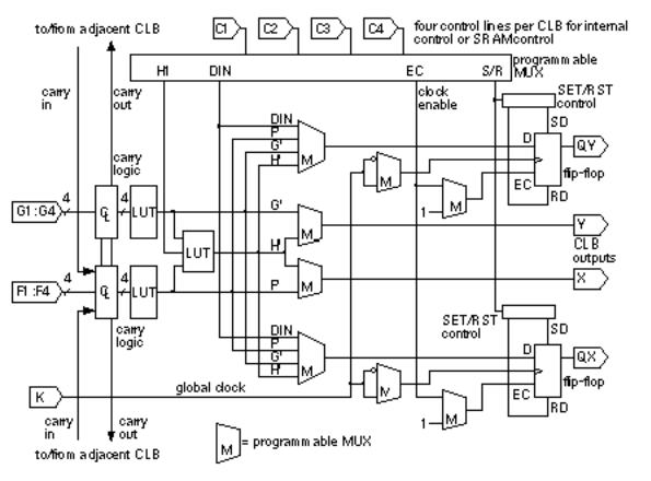
FIGURE 5.7 The Xilinx XC4000 family CLB (configurable logic block). ( Source: Xilinx.)
5.2.3 XC5200 Logic Block
Figure 5.8 shows the basic logic cell, a Logic Cell or LC, used in the XC5200
family of Xilinx LCA FPGAs. 1 The LC is similar to the CLBs in the XC2000/3000/4000 CLBs, but simpler. Xilinx retained the term CLB in the XC5200 to mean a group of four LCs (LC0 LC3).
The XC5200 LC contains a four-input LUT, a flip-flop, and MUXes to handle signal switching. The arithmetic carry logic is separate from the LUTs. A limited capability to cascade functions is provided (using the MUX labeled F5_MUX in logic cells LC0 and LC2 in Figure 5.8 ) to gang two LCs in parallel to provide the equivalent of a five-input LUT.
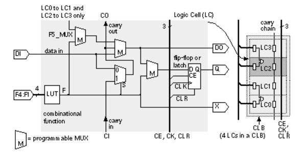
FIGURE 5.8 The Xilinx XC5200 family LC (Logic Cell) and CLB (configurable logic block). (Source: Xilinx.)
5.2.4 Xilinx CLB Analysis
The use of a LUT in a Xilinx CLB to implement combinational logic is both an advantage and a disadvantage. It means, for example, that an inverter is as slow as a five-input NAND. On the other hand a LUT simplifies timing of synchronous logic, simplifies the basic logic cell, and matches the Xilinx SRAM programming technology well. A LUT also provides the possibility, used in the XC4000, of using the LUT directly as SRAM. You can configure the XC4000 CLB as a memory either two 16 ¥ 1 SRAMs or a 32 ¥ 1 SRAM, but this is expensive RAM.
Figure 5.9 shows the timing model for Xilinx LCA FPGAs. 2 Xilinx uses two speed-grade systems. The first uses the maximum guaranteed toggle rate of a CLB flip-flop measured in MHz as a suffix so higher is faster. For example a Xilinx XC3020-125 has a toggle frequency of 125 MHz. The other Xilinx naming system (which supersedes the old scheme, since toggle frequency is rather meaningless) uses the approximate delay time of the combinational logic in a CLB in nanoseconds so lower is faster in this case. Thus, for example, an XC4010-6 has t ILO = 6.0 ns (the correspondence between speed grade and t ILO is fairly accurate for the XC2000, XC4000, and XC5200 but is less accurate for the XC3000).
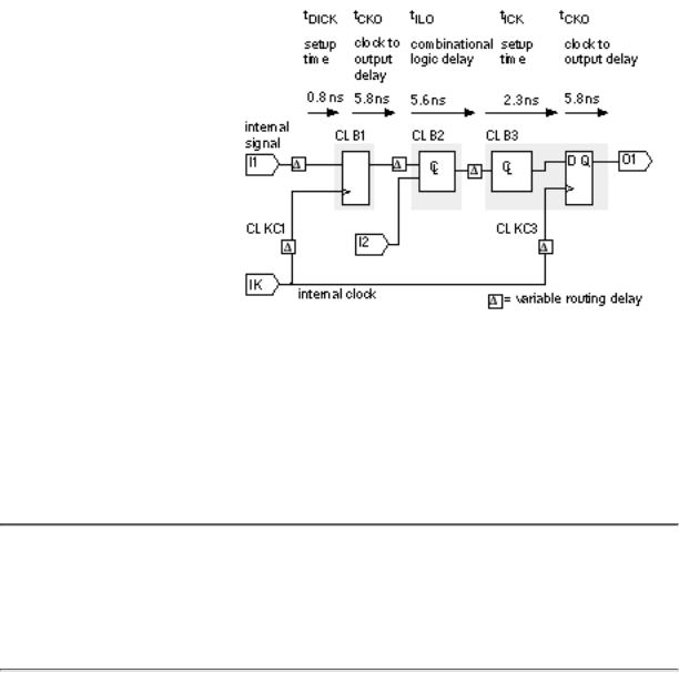
FIGURE 5.9 The Xilinx LCA timing model. The paths show different uses of CLBs (configurable logic blocks). The parameters shown are for an XC5210-6. ( Source: Xilinx.)
The inclusion of flip-flops and combinational logic inside the basic logic cell leads to efficient implementation of state machines, for example. The coarse-grain architecture of the Xilinx CLBs maximizes performance given the size of the SRAM programming technology element. As a result of the increased complexity of the basic logic cell we shall see (in Section 7.2, Xilinx LCA ) that the routing between cells is more complex than other FPGAs that use a simpler basic logic cell.
1.Xilinx decided to use Logic Cell as a trademark in 1995 rather as if IBM were to use Computer as a trademark today. Thus we should now only talk of a Xilinx Logic Cell (with capital letters) and not Xilinx logic cells.
2.October 1995 (Version 3.0) data sheet.