


7.3 Xilinx EPLD
The Xilinx EPLD family uses an interconnect bus known as Universal Interconnection Module ( UIM ) to distribute signals within the FPGA. The UIM, shown in Figure 7.7 , is a programmable AND array with constant delay from any input to any output. In Figure 7.7 :
●C G is the fixed gate capacitance of the EPROM device.
●C D is the fixed drain parasitic capacitance of the EPROM device.
●C B is the variable horizontal bus ( bit line) capacitance.
●C W is the variable vertical bus ( word line) capacitance.
Figure 7.7 shows the UIM has 21 output connections to each FB. 1 Thus the
XC7272 UIM (with a 4 ¥ 2 array of eight FBs as shown in Figure 7.7 ) has 168 (8 ¥ 21) output connections. Most (but not all) of the nine I/O cells attached to each FB have two input connections to the UIM, one from a chip input and one feedback from the macrocell output. For example, the XC7272 has 18 I/O cells that are outputs only and thus have only one connection to the UIM, so n = (18 ¥ 8) 18 = 126 input connections. Now we can calculate the number of tracks in the UIM: the XC7272, for example, has H = 126 tracks and V = 168/2 = 84 tracks. The actual physical height, V , of the UIM is determined by the size of the FBs, and is close to the die height.
The UIM ranges in size with the number of FBs. For the smallest XC7236 (with a 2 ¥ 2 array of four FBs), the UIM has n = 68 inputs and 84 outputs. For the XC73108 (with a 6 ¥ 2 array of 12 FBs), the UIM has n = 198 inputs. The UIM is a large array with large parasitic capacitance; it employs a highly optimized structure that uses EPROM devices and a sense amplifier at each output. The signal swing on the UIM uses less than the full V DD = 5 V to reduce the interconnect delay.
1. 1994 data book p. 3-62 and p. 3-78.
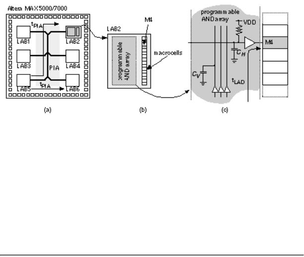
7.4 Altera MAX 5000 and 7000
Altera MAX 5000 devices (except the EPM5032, which has only one LAB) and all MAX 7000 devices use a Programmable Interconnect Array ( PIA ), shown in Figure 7.8 . The PIA is a cross-point switch for logic signals traveling between LABs. The advantages of this architecture (which uses a fixed number of connections) over programmable interconnection schemes (which use a variable number of connections) is the fixed routing delay. An additional benefit of the simpler nature of a large regular interconnect structure is the simplification and improved speed of the placement and routing software.
FIGURE 7.8 A simplified block diagram of the Altera MAX interconnect scheme. (a) The PIA (Programmable Interconnect Array) is deterministic delay is independent of the path length. (b) Each LAB (Logic Array Block) contains a programmable AND array. (c) Interconnect timing within a LAB is also fixed.
Figure 7.8 (a) illustrates that the delay between any two LABs, t PIA , is fixed. The delay between LAB1 and LAB2 (which are adjacent) is the same as the delay between LAB1 and LAB6 (on opposite corners of the die). It may seem rather strange to slow down all connections to the speed of the longest possible connection a large penalty to pay to achieve a deterministic architecture. However, it gives Altera the opportunity to highly optimize all of the connections since they are completely fixed.
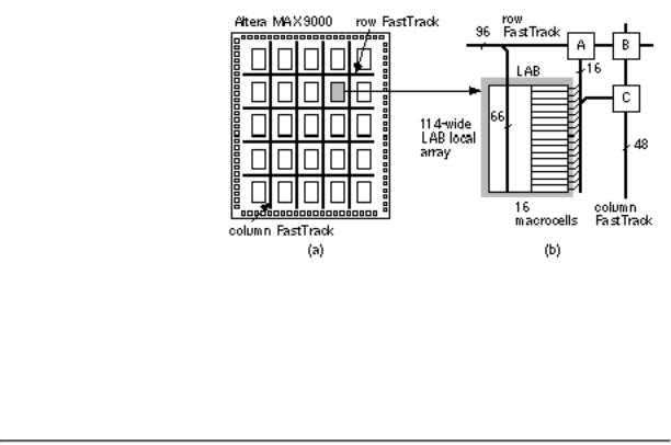
7.5 Altera MAX 9000
Figure 7.9 shows the Altera MAX 9000 interconnect architecture. The size of the MAX 9000 LAB arrays varies between 4 ¥ 5 (rows ¥ columns) for the EPM9320 and 7 ¥ 5 for the EPM9560. The MAX 9000 is an extremely coarse-grained architecture, typical of complex PLDs, but the LABs themselves have a finer structure. Sometimes we say that complex PLDs with arrays (LABs in the Altera MAX family) that are themselves arrays (of macrocells) have a dual-grain architecture .
FIGURE 7.9 The Altera MAX 9000 interconnect scheme. (a) A 4 ¥ 5 array of Logic Array Blocks (LABs), the same size as the EMP9400 chip. (b) A simplified block diagram of the interconnect architecture showing the connection of the FastTrack buses to a LAB.
In Figure 7.9 (b), boxes A, B, and C represent the interconnection between the FastTrack buses and the 16 macrocells in each LAB:
●Box A connects a macrocell to one row channel.
●Box B connects three column channels to two row channels.
●Box C connects a macrocell to three column channels.
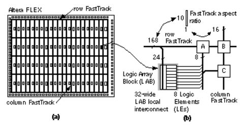
7.6 Altera FLEX
Figure 7.10 shows the interconnect used in the Altera FLEX family of complex PLDs. Altera refers to the FLEX interconnect and MAX 9000 interconnect by the same name, FastTrack, but the two are different because the granularity of the logic cell arrays is different. The FLEX architecture is of finer grain than the MAX arrays because of the difference in programming technology. The FLEX horizontal interconnect is much denser (at 168 channels per row) than the vertical interconnect (16 channels per column), creating an aspect ratio for the interconnect of over 10:1 (168:16). This imbalance is partly due to the aspect ratio of the die, the array, and the aspect ratio of the basic logic cell, the LAB.
FIGURE 7.10 The Altera FLEX interconnect scheme. (a) The row and column FastTrack interconnect. The chip shown, with 4 rows ¥ 21 columns, is the same size as the EPF8820. (b) A simplified diagram of the interconnect architecture showing the connections between the FastTrack buses and a LAB. Boxes A, B, and C represent the bus-to-bus connections.
As an example, the EPF8820 has 4 rows and 21 columns of LABs ( Figure 7.10 a). Ignoring, for simplicity s sake, what happens at the edge of the die we can total the routing channels as follows:
●Horizontal channels = 4 rows ¥ 168 channels/row = 672 channels.
●Vertical channels = 21 rows ¥ 16 channels/row = 336 channels.
It appears that there is still approximately twice (672:336) as much interconnect capacity in the horizontal direction as the vertical. If we look inside the boxes A, B, and C in Figure 7.10 (b) we see that for individual lines on each bus:

●Box A connects an LE to two row channels.
●Box B connects two column channels to a row channel.
●Box C connects an LE to two column channels.
There is some dependence between boxes A and B since they contain MUXes rather than direct connections, but essentially there are twice as many connections to the column FastTrack as the row FastTrack, thus restoring the balance in interconnect capacity.