

1.1 Types of ASICs
ICs are made on a thin (a few hundred microns thick), circular silicon wafer , with each wafer holding hundreds of die (sometimes people use dies or dice for the plural of die). The transistors and wiring are made from many layers (usually between 10 and 15 distinct layers) built on top of one another. Each successive mask layer has a pattern that is defined using a mask similar to a glass photographic slide. The first half-dozen or so layers define the transistors. The last half-dozen or so layers define the metal wires between the transistors (the interconnect ).
A full-custom IC includes some (possibly all) logic cells that are customized and all mask layers that are customized. A microprocessor is an example of a full-custom IC designers spend many hours squeezing the most out of every last square micron of microprocessor chip space by hand. Customizing all of the IC features in this way allows designers to include analog circuits, optimized memory cells, or mechanical structures on an IC, for example. Full-custom ICs are the most expensive to manufacture and to design. The manufacturing lead time (the time it takes just to make an IC not including design time) is typically eight weeks for a full-custom IC. These specialized full-custom ICs are often intended for a specific application, so we might call some of them full-custom ASICs.
We shall discuss full-custom ASICs briefly next, but the members of the IC family that we are more interested in are semicustom ASICs , for which all of the logic cells are predesigned and some (possibly all) of the mask layers are customized. Using predesigned cells from a cell library makes our lives as designers much, much easier. There are two types of semicustom ASICs that we shall cover: standard-cell based ASICs and gate-array based ASICs. Following this we shall describe the programmable ASICs , for which all of the logic cells are predesigned and none of the mask layers are customized. There are two types of programmable ASICs: the programmable logic device and, the newest member of the ASIC family, the field-programmable gate array.
1.1.1 Full-Custom ASICs
In a full-custom ASIC an engineer designs some or all of the logic cells, circuits, or layout specifically for one ASIC. This means the designer abandons the approach of using pretested and precharacterized cells for all or part of that design. It makes sense to take this approach only if there are no suitable existing
cell libraries available that can be used for the entire design. This might be because existing cell libraries are not fast enough, or the logic cells are not small enough or consume too much power. You may need to use full-custom design if the ASIC technology is new or so specialized that there are no existing cell libraries or because the ASIC is so specialized that some circuits must be custom designed. Fewer and fewer full-custom ICs are being designed because of the problems with these special parts of the ASIC. There is one growing member of this family, though, the mixed analog/digital ASIC, which we shall discuss next.
Bipolar technology has historically been used for precision analog functions. There are some fundamental reasons for this. In all integrated circuits the matching of component characteristics between chips is very poor, while the matching of characteristics between components on the same chip is excellent. Suppose we have transistors T1, T2, and T3 on an analog/digital ASIC. The three transistors are all the same size and are constructed in an identical fashion. Transistors T1 and T2 are located adjacent to each other and have the same orientation. Transistor T3 is the same size as T1 and T2 but is located on the other side of the chip from T1 and T2 and has a different orientation. ICs are made in batches called wafer lots. A wafer lot is a group of silicon wafers that are all processed together. Usually there are between 5 and 30 wafers in a lot. Each wafer can contain tens or hundreds of chips depending on the size of the IC and the wafer.
If we were to make measurements of the characteristics of transistors T1, T2, and T3 we would find the following:
●Transistors T1 will have virtually identical characteristics to T2 on the same IC. We say that the transistors match well or the tracking between devices is excellent.
●Transistor T3 will match transistors T1 and T2 on the same IC very well, but not as closely as T1 matches T2 on the same IC.
●Transistor T1, T2, and T3 will match fairly well with transistors T1, T2, and T3 on a different IC on the same wafer. The matching will depend on how far apart the two ICs are on the wafer.
●Transistors on ICs from different wafers in the same wafer lot will not match very well.
●Transistors on ICs from different wafer lots will match very poorly.
For many analog designs the close matching of transistors is crucial to circuit operation. For these circuit designs pairs of transistors are used, located adjacent to each other. Device physics dictates that a pair of bipolar transistors will always match more precisely than CMOS transistors of a comparable size. Bipolar technology has historically been more widely used for full-custom analog design because of its improved precision. Despite its poorer analog properties, the use of CMOS technology for analog functions is increasing. There are two reasons for this. The first reason is that CMOS is now by far the most widely available IC technology. Many more CMOS ASICs and CMOS standard products are now
being manufactured than bipolar ICs. The second reason is that increased levels of integration require mixing analog and digital functions on the same IC: this has forced designers to find ways to use CMOS technology to implement analog functions. Circuit designers, using clever new techniques, have been very successful in finding new ways to design analog CMOS circuits that can approach the accuracy of bipolar analog designs.
1.1.2 Standard-Cell Based ASICs
A cell-based ASIC (cell-based IC, or CBIC a common term in Japan, pronounced sea-bick ) uses predesigned logic cells (AND gates, OR gates, multiplexers, and flip-flops, for example) known as standard cells . We could apply the term CBIC to any IC that uses cells, but it is generally accepted that a cell-based ASIC or CBIC means a standard-cell based ASIC.
The standard-cell areas (also called flexible blocks) in a CBIC are built of rows of standard cells like a wall built of bricks. The standard-cell areas may be used in combination with larger predesigned cells, perhaps microcontrollers or even microprocessors, known as megacells . Megacells are also called megafunctions, full-custom blocks, system-level macros (SLMs), fixed blocks, cores, or Functional Standard Blocks (FSBs).
The ASIC designer defines only the placement of the standard cells and the interconnect in a CBIC. However, the standard cells can be placed anywhere on the silicon; this means that all the mask layers of a CBIC are customized and are unique to a particular customer. The advantage of CBICs is that designers save time, money, and reduce risk by using a predesigned, pretested, and precharacterized standard-cell library . In addition each standard cell can be optimized individually. During the design of the cell library each and every transistor in every standard cell can be chosen to maximize speed or minimize area, for example. The disadvantages are the time or expense of designing or buying the standard-cell library and the time needed to fabricate all layers of the ASIC for each new design.
Figure 1.2 shows a CBIC (looking down on the die shown in Figure 1.1b, for example). The important features of this type of ASIC are as follows:
●All mask layers are customized transistors and interconnect.
●Custom blocks can be embedded.
●Manufacturing lead time is about eight weeks.
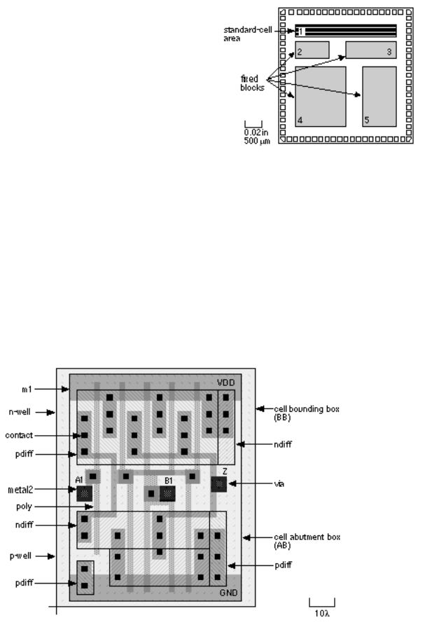
FIGURE 1.2 A cell-based ASIC (CBIC) die with a single standard-cell area (a flexible block) together with four fixed blocks. The flexible block contains rows of standard cells. This is what you might see through a low-powered microscope looking down on the die of Figure 1.1(b). The small squares around the edge of the die are bonding pads that are connected to the pins of the ASIC package.
Each standard cell in the library is constructed using full-custom design methods, but you can use these predesigned and precharacterized circuits without having to do any full-custom design yourself. This design style gives you the same performance and flexibility advantages of a full-custom ASIC but reduces design time and reduces risk.
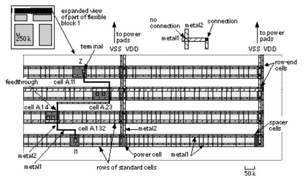
Standard cells are designed to fit together like bricks in a wall. Figure 1.3 shows an example of a simple standard cell (it is simple in the sense it is not maximized for density but ideal for showing you its internal construction). Power and ground buses (VDD and GND or VSS) run horizontally on metal lines inside the cells.
FIGURE 1.3 Looking down on the layout of a standard cell. This cell would be approximately 25 microns wide on an ASIC with l (lambda) = 0.25 microns (a micron is 10 6 m). Standard cells are stacked like bricks in a wall; the abutment box (AB) defines the edges of the brick. The difference between the bounding box (BB) and the AB is the area of overlap between the bricks. Power supplies (labeled VDD and GND) run horizontally inside a standard cell on a metal layer that lies above the transistor layers. Each different shaded and labeled pattern represents a different layer. This standard cell has center connectors (the three squares, labeled A1, B1, and Z) that allow the cell to connect to others. The layout was drawn using ROSE, a symbolic layout editor developed by Rockwell and Compass, and then imported into Tanner Research s L-Edit.
Standard-cell design allows the automation of the process of assembling an ASIC. Groups of standard cells fit horizontally together to form rows. The rows stack vertically to form flexible rectangular blocks (which you can reshape during design). You may then connect a flexible block built from several rows of standard cells to other standard-cell blocks or other full-custom logic blocks. For example, you might want to include a custom interface to a standard, predesigned microcontroller together with some memory. The microcontroller block may be a fixed-size megacell, you might generate the memory using a memory compiler, and the custom logic and memory controller will be built from flexible standard-cell blocks, shaped to fit in the empty spaces on the chip.
Both cell-based and gate-array ASICs use predefined cells, but there is a difference we can change the transistor sizes in a standard cell to optimize speed and performance, but the device sizes in a gate array are fixed. This results in a trade-off in performance and area in a gate array at the silicon level. The trade-off between area and performance is made at the library level for a standard-cell ASIC.
Modern CMOS ASICs use two, three, or more levels (or layers) of metal for interconnect. This allows wires to cross over different layers in the same way that we use copper traces on different layers on a printed-circuit board. In a two-level metal CMOS technology, connections to the standard-cell inputs and outputs are usually made using the second level of metal ( metal2 , the upper level of metal) at the tops and bottoms of the cells. In a three-level metal technology, connections may be internal to the logic cell (as they are in Figure 1.3). This allows for more sophisticated routing programs to take advantage of the extra metal layer to route interconnect over the top of the logic cells. We shall cover the details of routing ASICs in Chapter 17.
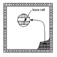
A connection that needs to cross over a row of standard cells uses a feedthrough. The term feedthrough can refer either to the piece of metal that is used to pass a signal through a cell or to a space in a cell waiting to be used as a feedthroughvery confusing. Figure 1.4 shows two feedthroughs: one in cell A.14 and one in cell A.23.
In both two-level and three-level metal technology, the power buses (VDD and GND) inside the standard cells normally use the lowest (closest to the transistors) layer of metal ( metal1 ). The width of each row of standard cells is adjusted so that they may be aligned using spacer cells . The power buses, or rails, are then connected to additional vertical power rails using row-end cells at the aligned ends of each standard-cell block. If the rows of standard cells are long, then vertical power rails can also be run in metal2 through the cell rows using special power cells that just connect to VDD and GND. Usually the designer manually controls the number and width of the vertical power rails connected to the standard-cell blocks during physical design. A diagram of the power distribution scheme for a CBIC is shown in Figure 1.4.
FIGURE 1.4 Routing the CBIC (cell-based IC) shown in Figure 1.2. The use of regularly shaped standard cells, such as the one in Figure 1.3, from a library allows ASICs like this to be designed automatically. This ASIC uses two separate layers of metal interconnect (metal1 and metal2) running at right angles to each other (like traces on a printed-circuit board). Interconnections between logic cells uses spaces (called channels) between the rows of cells. ASICs may have three (or more) layers of metal allowing the cell rows to touch with the interconnect running over the top of the cells.
All the mask layers of a CBIC are customized. This allows megacells (SRAM, a SCSI controller, or an MPEG decoder, for example) to be placed on the same IC with standard cells. Megacells are usually supplied by an ASIC or library company complete with behavioral models and some way to test them (a test strategy). ASIC library companies also supply compilers to generate flexible DRAM, SRAM, and ROM blocks. Since all mask layers on a standard-cell design are customized, memory design is more efficient and denser than for gate arrays.
For logic that operates on multiple signals across a data bus a datapath ( DP ) the use of standard cells may not be the most efficient ASIC design style. Some ASIC library companies provide a datapath compiler that automatically generates datapath logic . A datapath library typically contains cells such as adders, subtracters, multipliers, and simple arithmetic and logical units ( ALUs ). The connectors of datapath library cells are pitch-matched to each other so that they fit together. Connecting datapath cells to form a datapath usually, but not always, results in faster and denser layout than using standard cells or a gate array.
Standard-cell and gate-array libraries may contain hundreds of different logic cells, including combinational functions (NAND, NOR, AND, OR gates) with multiple inputs, as well as latches and flip-flops with different combinations of reset, preset and clocking options. The ASIC library company provides designers with a data book in paper or electronic form with all of the functional descriptions and timing information for each library element.
1.1.3 Gate-Array Based ASICs
In a gate array (sometimes abbreviated to GA) or gate-array based ASIC the transistors are predefined on the silicon wafer. The predefined pattern of transistors on a gate array is the base array , and the smallest element that is replicated to make the base array (like an M. C. Escher drawing, or tiles on a floor) is the base cell (sometimes called a primitive cell ). Only the top few layers of metal, which define the interconnect between transistors, are defined by the designer using custom masks. To distinguish this type of gate array from other types of gate array, it is often called a masked gate array ( MGA ). The designer chooses from a gate-array library of predesigned and precharacterized logic cells. The logic cells in a gate-array library are often called macros . The reason for this is that the base-cell layout is the same for each logic cell, and only the interconnect (inside cells and between cells) is customized, so that there is a similarity between gate-array macros and a software macro. Inside IBM, gate-array macros are known as books (so that books are part of a library), but unfortunately this descriptive term is not very widely used outside IBM.
We can complete the diffusion steps that form the transistors and then stockpile wafers (sometimes we call a gate array a prediffused array for this reason). Since only the metal interconnections are unique to an MGA, we can use the stockpiled wafers for different customers as needed. Using wafers prefabricated up to the metallization steps reduces the time needed to make an MGA, the turnaround time , to a few days or at most a couple of weeks. The costs for all the initial fabrication steps for an MGA are shared for each customer and this reduces the cost of an MGA compared to a full-custom or standard-cell ASIC design.
There are the following different types of MGA or gate-array based ASICs:
●Channeled gate arrays.
●Channelless gate arrays.
● Structured gate arrays.
The hyphenation of these terms when they are used as adjectives explains their construction. For example, in the term channeled gate-array architecture, the gate array is channeled , as will be explained. There are two common ways of arranging (or arraying) the transistors on a MGA: in a channeled gate array we leave space between the rows of transistors for wiring; the routing on a channelless gate array uses rows of unused transistors. The channeled gate array was the first to be developed, but the channelless gate-array architecture is now more widely used. A structured (or embedded) gate array can be either channeled or channelless but it includes (or embeds) a custom block.
1.1.4 Channeled Gate Array
Figure 1.5 shows a channeled gate array . The important features of this type of MGA are:
●Only the interconnect is customized.
●The interconnect uses predefined spaces between rows of base cells.
●Manufacturing lead time is between two days and two weeks.
FIGURE 1.5 A channeled gate-array die. The spaces between rows of the base cells are set aside for interconnect.
A channeled gate array is similar to a CBIC both use rows of cells separated by channels used for interconnect. One difference is that the space for interconnect between rows of cells are fixed in height in a channeled gate array, whereas the space between rows of cells may be adjusted in a CBIC.
1.1.5 Channelless Gate Array
Figure 1.6 shows a channelless gate array (also known as a channel-free gate array , sea-of-gates array , or SOG array). The important features of this type of MGA are as follows:
●Only some (the top few) mask layers are customized the interconnect.
●Manufacturing lead time is between two days and two weeks.
FIGURE 1.6 A channelless gate-array or sea-of-gates (SOG) array die. The core area of the die is completely filled with an array of base cells (the base array).
The key difference between a channelless gate array and channeled gate array is that there are no predefined areas set aside for routing between cells on a channelless gate array. Instead we route over the top of the gate-array devices. We can do this because we customize the contact layer that defines the connections between metal1, the first layer of metal, and the transistors. When we use an area of transistors for routing in a channelless array, we do not make any contacts to the devices lying underneath; we simply leave the transistors unused.
The logic density the amount of logic that can be implemented in a given silicon area is higher for channelless gate arrays than for channeled gate arrays. This is usually attributed to the difference in structure between the two types of array. In fact, the difference occurs because the contact mask is customized in a channelless gate array, but is not usually customized in a channeled gate array. This leads to denser cells in the channelless architectures. Customizing the contact layer in a channelless gate array allows us to increase the density of gate-array cells because we can route over the top of unused contact sites.
1.1.6 Structured Gate Array
An embedded gate array or structured gate array (also known as masterslice or masterimage ) combines some of the features of CBICs and MGAs. One of the disadvantages of the MGA is the fixed gate-array base cell. This makes the implementation of memory, for example, difficult and inefficient. In an embedded gate array we set aside some of the IC area and dedicate it to a specific function. This embedded area either can contain a different base cell that is more suitable for building memory cells, or it can contain a complete circuit block, such as a microcontroller.
Figure 1.7 shows an embedded gate array. The important features of this type of MGA are the following:
●Only the interconnect is customized.
●Custom blocks (the same for each design) can be embedded.
●Manufacturing lead time is between two days and two weeks.
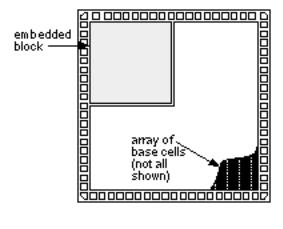
FIGURE 1.7 A structured or embedded gate-array die showing an embedded block in the upper left corner (a static random-access memory, for example). The rest of the die is filled with an array of base cells.
An embedded gate array gives the improved area efficiency and increased performance of a CBIC but with the lower cost and faster turnaround of an MGA. One disadvantage of an embedded gate array is that the embedded function is fixed. For example, if an embedded gate array contains an area set aside for a 32 k-bit memory, but we only need a 16 k-bit memory, then we may have to waste half of the embedded memory function. However, this may still be more efficient and cheaper than implementing a 32 k-bit memory using macros on a SOG array.
ASIC vendors may offer several embedded gate array structures containing different memory types and sizes as well as a variety of embedded functions. ASIC companies wishing to offer a wide range of embedded functions must ensure that enough customers use each different embedded gate array to give the cost advantages over a custom gate array or CBIC (the Sun Microsystems SPARCstation 1 described in Section 1.3 made use of LSI Logic embedded gate arrays and the 10K and 100K series of embedded gate arrays were two of LSI Logic s most successful products).
1.1.7 Programmable Logic Devices
Programmable logic devices ( PLDs ) are standard ICs that are available in standard configurations from a catalog of parts and are sold in very high volume to many different customers. However, PLDs may be configured or programmed to create a part customized to a specific application, and so they also belong to the family of ASICs. PLDs use different technologies to allow programming of the device. Figure 1.8 shows a PLD and the following important features that all PLDs have in common:
●No customized mask layers or logic cells
●Fast design turnaround
●A single large block of programmable interconnect
●A matrix of logic macrocells that usually consist of programmable array logic followed by a flip-flop or latch
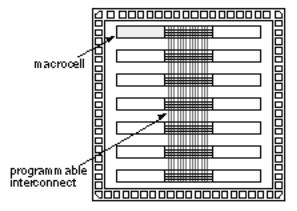
FIGURE 1.8 A programmable logic device (PLD) die. The macrocells typically consist of programmable array logic followed by a flip-flop or latch. The macrocells are connected using a large programmable interconnect block.
The simplest type of programmable IC is a read-only memory ( ROM ). The most common types of ROM use a metal fuse that can be blown permanently (a programmable ROM or PROM ). An electrically programmable ROM , or EPROM , uses programmable MOS transistors whose characteristics are altered by applying a high voltage. You can erase an EPROM either by using another high voltage (an electrically erasable PROM , or EEPROM ) or by exposing the device to ultraviolet light ( UV-erasable PROM , or UVPROM ).
There is another type of ROM that can be placed on any ASIC a mask-programmable ROM (mask-programmed ROM or masked ROM). A masked ROM is a regular array of transistors permanently programmed using custom mask patterns. An embedded masked ROM is thus a large, specialized, logic cell.
The same programmable technologies used to make ROMs can be applied to more flexible logic structures. By using the programmable devices in a large array of AND gates and an array of OR gates, we create a family of flexible and programmable logic devices called logic arrays . The company Monolithic Memories (bought by AMD) was the first to produce Programmable Array Logic (PAL ® , a registered trademark of AMD) devices that you can use, for example, as transition decoders for state machines. A PAL can also include registers (flip-flops) to store the current state information so that you can use a PAL to make a complete state machine.
Just as we have a mask-programmable ROM, we could place a logic array as a cell on a custom ASIC. This type of logic array is called a programmable logic array (PLA). There is a difference between a PAL and a PLA: a PLA has a programmable AND logic array, or AND plane , followed by a programmable OR logic array, or OR plane ; a PAL has a programmable AND plane and, in contrast to a PLA, a fixed OR plane.
Depending on how the PLD is programmed, we can have an erasable PLD (EPLD), or mask-programmed PLD (sometimes called a masked PLD but usually just PLD). The first PALs, PLAs, and PLDs were based on bipolar technology and used programmable fuses or links. CMOS PLDs usually employ floating-gate transistors (see Section 4.3, EPROM and EEPROM Technology ).
1.1.8 Field-Programmable Gate Arrays
A step above the PLD in complexity is the field-programmable gate array ( FPGA ). There is very little difference between an FPGA and a PLD an FPGA is usually just larger and more complex than a PLD. In fact, some companies that manufacture programmable ASICs call their products FPGAs and some call them complex PLDs . FPGAs are the newest member of the ASIC family and are rapidly growing in importance, replacing TTL in microelectronic systems. Even though an FPGA is a type of gate array, we do not consider the term gate-arraybased ASICs to include FPGAs. This may change as FPGAs and MGAs start to look more alike.
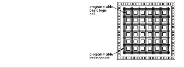
Figure 1.9 illustrates the essential characteristics of an FPGA:
●None of the mask layers are customized.
●A method for programming the basic logic cells and the interconnect.
●The core is a regular array of programmable basic logic cells that can implement combinational as well as sequential logic (flip-flops).
●A matrix of programmable interconnect surrounds the basic logic cells.
●Programmable I/O cells surround the core.
●Design turnaround is a few hours.
We shall examine these features in detail in Chapters 4 8.
FIGURE 1.9 A field-programmable gate array (FPGA) die. All FPGAs contain a regular structure of programmable basic logic cells surrounded by programmable interconnect. The exact type, size, and number of the programmable basic logic cells varies tremendously.