

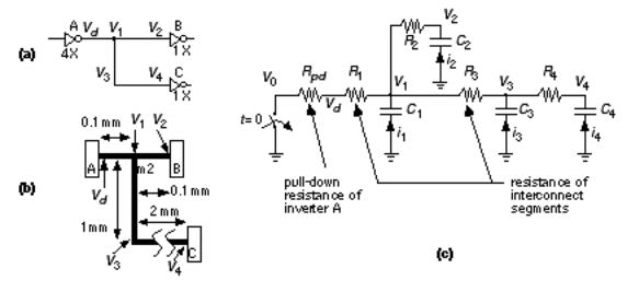
predefined look-up table. After placement, the logic cell positions are fixed and the global router can afford to use better estimates of the interconnect delay. To illustrate one method, we shall use the Elmore constant to estimate the interconnect delay for the circuit shown in Figure 17.3 .
FIGURE 17.3 Measuring the delay of a net. (a) A simple circuit with an inverter A driving a net with a fanout of two. Voltages V 1 , V 2 , V 3 , and V 4 are the voltages at intermediate points along the net. (b) The layout showing the net segments (pieces of interconnect). (c) The RC model with each segment replaced by a capacitance and resistance. The ideal switch and pull-down resistance R pd model the inverter A.
The problem is to find the voltages at the inputs to logic cells B and C taking into account the parasitic resistance and capacitance of the metal interconnect.
Figure 17.3 (c) models logic cell A as an ideal switch with a pull-down resistance equal to R pd and models the metal interconnect using resistors and capacitors for each segment of the interconnect.
The Elmore constant for node 4 (labeled V 4 ) in the network shown in Figure 17.3 (c) is
4 |
|
|
t D 4 = S |
R k 4 C k |
(17.1) |
k = 1 |
|
|
|
= R 14 C 1 + R 24 C 2 + R 34 C 3 + R 44 C 4 , |
|
where, |
|
|
R 14 |
= R pd + R 1 |
(17.2) |
R 24 |
= R pd + R 1 |
|
R 34 = R pd + R 1 + R 3 |
|
|

R 44 = R pd + R 1 + R 3 + R 4
In Eq. 17.2 notice that R 24 = R pd + R 1 (and not R pd + R 1 + R 2 ) because R 1 is the resistance to V 0 (ground) shared by node 2 and node 4.
Suppose we have the following parameters (from the generic 0.5 m m CMOS process, G5) for the layout shown in Figure 17.3 (b):
●m2 resistance is 50 m W /square.
●m2 capacitance (for a minimum-width line) is 0.2 pFmm 1 .
●4X inverter delay is 0.02 ns + 0.5 C L ns ( C L is in picofarads).
●Delay is measured using 0.35/0.65 output trip points.
●m2 minimum width is 3 l = 0.9 m m.
●1X inverter input capacitance is 0.02 pF (a standard load).
First we need to find the pull-down resistance, R pd , of the 4X inverter. If we model the gate with a linear pull-down resistor, R pd , driving a load C L , the output waveform is exp t /( C L R pd ) (normalized to 1V). The output reaches 63 percent of its final value when t = C L R pd , because exp ( 1) = 0.63. Then,
because the delay is measured with a 0.65 trip point, the constant 0.5 nspF 1 = 0.5 k W is very close to the equivalent pull-down resistance. Thus, R pd ª 500 W .
From the given data, we can calculate the R s and C s:
|
(0.1 mm) (50 ¥ 10 3 W ) |
|
|
R 1 = R 2 = |
= 6 W |
|
|
|
0.9 m m |
|
|
|
(1 mm) (50 ¥ 10 3 W ) |
|
|
R 3 |
= |
= 56 W |
|
|
0.9 m m |
|
|
|
(2 mm) (50 ¥ 10 3 W ) |
|
|
R 4 |
= |
= 112 W |
|
|
0.9 m m |
|
|
|
|
|
(17.3) |
C 1 = (0.1 mm) (0.2 ¥ pFmm 1 ) |
= |
0.02 pF |
|
C 2 = (0.1 mm) (0.2 ¥ pFmm 1 ) + 0.02 pF = |
0.04 pF |
||
C 3 |
= (1 mm) (0.2 ¥ pFmm 1 ) |
= |
0.2 pF |
C 4 |
= (2 mm) (0.2 ¥ pFmm 1 ) + 0.02 pF = |
0.42 pF |
|
(17.4)
Now we can calculate the path resistance, R ki , values (notice that R ki = R ik ):
R 14 |
= 500 W + 6 W |
= 506 W |
R 24 |
= 500 W + 6 W |
= 506 W |
R 34 |
= 500 W + 6 W + 56 W |
= 562 W |
R 44 |
= 500 W + 6 W + 56 W + 112 W = 674 W |
|
(17.5)
Finally, we can calculate Elmore s constants for node 4 and node 2 as follows:
t D 4 = R 14 C 1 + R 24 C 2 + R 34 C 3 + R 44 C 4 (17.6)
=(506)(0.02) + (506)(0.04) + (562)(0.2) + (674)(0.42)
=425 ps .
t D 2 = R 12 C 1 + R 22 C 2 + R 32 C 3 + R 42 C 4 (17.7)
=( R pd + R 1 )( C 2 + C 3 + C 4 )
+( R pd + R 1 + R 2 ) C 2
=(500 + 6 + 6)(0.04)
+(500 + 6)(0.02 + 0.2 + 0.2)
=344 ps .
and t D 4 t D 2 = (425 344) = 81 ps.
A lumped-delay model neglects the effects of interconnect resistance and simply sums all the node capacitances (the lumped capacitance ) as follows:
t D = R pd ( C 1 + C 2 + C 3 + C 4 ) |
(17.8) |
=(500) (0.02 + 0.04 + 0.2 + 0.42)
=340 ps .
Comparing Eqs. 17.6 17.8 , we can see that the delay of the inverter can be
assigned as follows: 20 ps (the intrinsic delay, 0.2 ns, due to the cell output capacitance), 340 ps (due to the pull-down resistance and the output capacitance), 4 ps (due to the interconnect from A to B), and 65 ps (due to the interconnect from A to C). We can see that the error from neglecting interconnect resistance can be important.
Even using the Elmore constant we still made the following assumptions in estimating the path delays:
●A step-function waveform drives the net.
●The delay is measured from when the gate input changes.
●The delay is equal to the time constant of an exponential waveform that approximates the actual output waveform.
●The interconnect is modeled by discrete resistance and capacitance elements.
The global router could use more sophisticated estimates that remove some of these assumptions, but there is a limit to the accuracy with which delay can be estimated during global routing. For example, the global router does not know how much of the routing is on which of the layers, or how many vias will be used and of which type, or how wide the metal lines will be. It may be possible to estimate how much interconnect will be horizontal and how much is vertical. Unfortunately, this knowledge does not help much if horizontal interconnect may be completed in either m1 or m3 and there is a large difference in parasitic capacitance between m1 and m3, for example.
When the global router attempts to minimize interconnect delay, there is an important difference between a path and a net. The path that minimizes the delay between two terminals on a net is not necessarily the same as the path that minimizes the total path length of the net. For example, to minimize the path delay (using the Elmore constant as a measure) from the output of inverter A in Figure 17.3 (a) to the input of inverter B requires a rather complicated algorithm to construct the best path. We shall return to this problem in Section 17.1.6 .
17.1.3 Global Routing Methods
Global routing cannot use the interconnect-length approximations, such as the half-perimeter measure, that were used in placement. What is needed now is the actual path and not an approximation to the path length. However, many of the methods used in global routing are still based on the solutions to the tree on a graph problem.
One approach to global routing takes each net in turn and calculates the shortest path using tree on graph algorithms with the added restriction of using the available channels. This process is known as sequential routing . As a sequential routing algorithm proceeds, some channels will become more congested since they hold more interconnects than others. In the case of FPGAs and channeled gate arrays, the channels have a fixed channel capacity and can only hold a certain number of interconnects. There are two different ways that a global router normally handles this problem. Using order-independent routing , a global router proceeds by routing each net, ignoring how crowded the channels are. Whether a particular net is processed first or last does not matter, the channel assignment will be the same. In order-independent routing, after all the interconnects are assigned to channels, the global router returns to those channels that are the most crowded and reassigns some interconnects to other, less crowded, channels. Alternatively, a global router can consider the number of interconnects already placed in various channels as it proceeds. In this case the global routing is order
dependent the routing is still sequential, but now the order of processing the nets will affect the results. Iterative improvement or simulated annealing may be applied to the solutions found from both order-dependent and order-independent algorithms. This is implemented in the same way as for system partitioning and placement: A constructed solution is successively changed, one interconnect path at a time, in a series of random moves.
In contrast to sequential global-routing methods, which handle nets one at a time, hierarchical routing handles all nets at a particular level at once. Rather than handling all of the nets on the chip at the same time, the global-routing problem is made more tractable by dividing the chip area into levels of hierarchy. By considering only one level of hierarchy at a time the size of the problem is reduced at each level. There are two ways to traverse the levels of hierarchy. Starting at the whole chip, or highest level, and proceeding down to the logic cells is the top-down approach. The bottom-up approach starts at the lowest level of hierarchy and globally routes the smallest areas first.
17.1.4 Global Routing Between Blocks
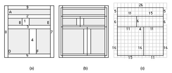
Figure 17.4 illustrates the global-routing problem for a cell-based ASIC. Each edge in the channel-intersection graph in Figure 17.4 (c) represents a channel. The global router is restricted to using these channels. The weight of each edge in the graph corresponds to the length of the channel. The global router plans a path for each interconnect using this graph.
FIGURE 17.4 Global routing for a cell-based ASIC formulated as a graph problem. (a) A cell-based ASIC with numbered channels. (b) The channels form the edges of a graph. (c) The channel-intersection graph. Each channel corresponds to an edge on a graph whose weight corresponds to the channel length.
Figure 17.5 shows an example of global routing for a net with five terminals, labeled A1 through F1, for the cell-based ASIC shown in Figure 17.4 . If a designer wishes to use minimum total interconnect path length as an objective,

the global router finds the minimum-length tree shown in Figure 17.5 (b). This tree determines the channels the interconnects will use. For example, the shortest connection from A1 to B1 uses channels 2, 1, and 5 (in that order). This is the information the global router passes to the detailed router. Figure 17.5 (c) shows that minimizing the total path length may not correspond to minimizing the path delay between two points.
FIGURE 17.5 Finding paths in global routing. (a) A cell-based ASIC (from Figure 17.4 ) showing a single net with a fanout of four (five terminals). We have to order the numbered channels to complete the interconnect path for terminals A1 through F1. (b) The terminals are projected to the center of the nearest channel, forming a graph. A minimum-length tree for the net that uses the channels and takes into account the channel capacities. (c) The minimum-length tree does not necessarily correspond to minimum delay. If we wish to minimize the delay from terminal A1 to D1, a different tree might be better.
Global routing is very similar for cell-based ASICs and gate arrays, but there is a very important difference between the types of channels in these ASICs. The size of the channels in sea-of-gates arrays, channelless gate arrays, and cell-based ASICs can be varied to make sure there is enough space to complete the wiring. In channeled gate-arrays and FPGAs the size, number, and location of channels are fixed. The good news is that the global router can allocate as many interconnects to each channel as it likes, since that space is committed anyway. The bad news is that there is a maximum number of interconnects that each channel can hold. If the global router needs more room, even in just one channel on the whole chip, the designer has to repeat the placement-and-routing steps and try again (or use a bigger chip).
17.1.5 Global Routing Inside Flexible
Blocks
We shall illustrate global routing using a gate array. Figure 17.6 (a) shows the routing resources on a sea-of-gates or channelless gate array. The gate array base cells are arranged in 36 blocks, each block containing an array of 8-by-16 gate-array base cells, making a total of 4068 base cells.
The horizontal interconnect resources are the routing channels that are formed from unused rows of the gate-array base cells, as shown in Figure 17.6 (b) and
(c). The vertical resources are feedthroughs. For example, the logic cell shown in Figure 17.6 (d) is an inverter that contains two types of feedthrough. The inverter logic cell uses a single gate-array base cell with terminals (or connectors ) located at the top and bottom of the logic cell. The inverter input pin has two electrically equivalent terminals that the global router can use as a feedthrough. The output of the inverter is connected to only one terminal. The remaining vertical track is unused by the inverter logic cell, so this track forms an uncommitted feedthrough.
You may see any of the terms landing pad (because we say that we drop a via to a landing pad), pick-up point , connector , terminal , pin , or port used for the connection to a logic cell. The term pick-up point refers to the physical pieces of metal (or sometimes polysilicon) in the logic cell to which the router connects. In a three-level metal process, the global router may be able to connect to anywhere in an area an area pick-up point . In this book we use the term connector to refer to the physical pick-up point. The term pin more often refers to the connection on a logic schematic icon (a dot, square box, or whatever symbol is used), rather than layout. Thus the difference between a pin and a connector is that we can have multiple connectors for one pin. Terminal is often used when we talk about routing. The term port is used when we are using text (EDIF netlists or HDLs, for example) to describe circuits.
In a gate array the channel capacity must be a multiple of the number of horizontal tracks in the gate-array base cell. Figure 17.6 (e) shows a gate-array base cell with seven horizontal tracks (see Section 17.2 for the factors that determine the track width and track spacing). Thus, in this gate array, we can have a channel with a capacity of 7, 14, 21, ... horizontal tracks but not between these values.
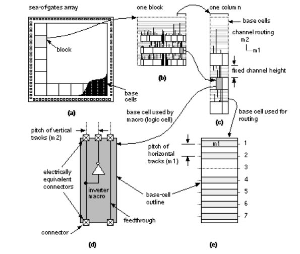
FIGURE 17.6 Gate-array global routing. (a) A small gate array. (b) An enlarged view of the routing. The top channel uses three rows of gate-array base cells; the other channels use only one. (c) A further enlarged view showing how the routing in the channels connects to the logic cells. (d) One of the logic cells, an inverter. (e) There are seven horizontal wiring tracks available in one row of gate-array base cells the channel capacity is thus 7.
Figure 17.7 shows the inverter macro for the sea-of-gates array shown in Figure 17.6 . Figure 17.7 (a) shows the base cell. Figure 17.7 (b) shows how the
internal inverter wiring on m1 leaves one vertical track free as a feedthrough in a two-level metal process (connectors placed at the top and bottom of the cell). In a three-level metal process the connectors may be placed inside the cell abutment box ( Figure 17.7 c). Figure 17.8 shows the global routing for the sea-of-gates array. We divide the array into nonoverlapping routing bins (or just bins , also called global routing cells or GRCs ), each containing a number of gate-array base cells.
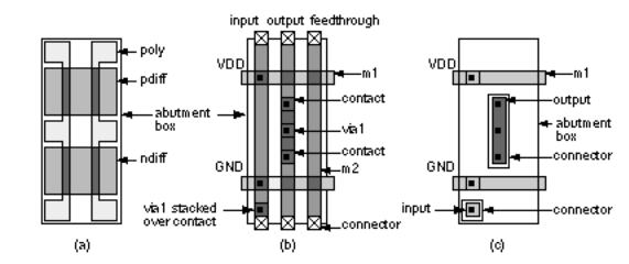
FIGURE 17.7 The gate-array inverter from Figure 17.6 d. (a) An oxide-isolated gate-array base cell, showing the diffusion and polysilicon layers. (b) The metal and contact layers for the inverter in a 2LM (two-level metal) process. (c) The router s view of the cell in a 3LM process.
We need an aside to discuss our use of the term cell . Be careful not to confuse the global routing cells with gate-array base cells (the smallest element of a gate array, consisting of a small number of n -type and p -type transistors), or with logic cells (which are NAND gates, NOR gates, and so on).
A large routing bin reduces the size of the routing problem, and a small routing bin allows the router to calculate the wiring capacities more accurately. Some tools permit routing bins of different size in different areas of the chip (with smaller routing bins helping in areas of dense routing). Figure 17.8 (a) shows a routing bin that is 2 -by-4 gate-array base cells. The logic cells occupy the lower half of the routing bin. The upper half of the routing bin is the channel area, reserved for wiring. The global router calculates the edge capacities for this routing bin, including the vertical feedthroughs. The global router then determines the shortest path for each net considering these edge capacities. An example of a global-routing calculation is shown in Figure 17.8 (b). The path, described by a series of adjacent routing bins, is passed to the detailed router.
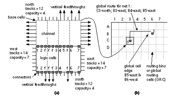
FIGURE 17.8 Global routing a gate array. (a) A single global-routing cell (GRC or routing bin) containing 2-by-4 gate-array base cells. For this choice of routing bin the maximum horizontal track capacity is 14, the maximum vertical track capacity is 12. The routing bin labeled C3 contains three logic cells, two of which have feedthroughs marked 'f'. This results in the edge capacities shown.
(b) A view of the top left-hand corner of the gate array showing 28 routing bins. The global router uses the edge capacities to find a sequence of routing bins to connect the nets.
17.1.6 Timing-Driven Methods
Minimizing the total pathlength using a Steiner tree does not necessarily minimize the interconnect delay of a path. Alternative tree algorithms apply in this situation, most using the Elmore constant as a method to estimate the delay of a path ( Section 17.1.2 ). As in timing-driven placement, there are two main approaches to timing-driven routing: net-based and path-based. Path-based methods are more sophisticated. For example, if there is a critical path from logic cell A to B to C, the global router may increase the delay due to the interconnect between logic cells A and B if it can reduce the delay between logic cells B and C. Placement and global routing tools may or may not use the same algorithm to estimate net delay. If these tools are from different companies, the algorithms are probably different. The algorithms must be compatible, however. There is no use performing placement to minimize predicted delay if the global router uses completely different measurement methods. Companies that produce floorplanning and placement tools make sure that the output is compatible with different routing tools often to the extent of using different algorithms to target different routers.

17.1.7 Back-annotation
After global routing is complete it is possible to accurately predict what the length of each interconnect in every net will be after detailed routing, probably to within 5 percent. The global router can give us not just an estimate of the total net length (which was all we knew at the placement stage), but the resistance and capacitance of each path in each net. This RC information is used to calculate net delays. We can back-annotate this net delay information to the synthesis tool for in-place optimization or to a timing verifier to make sure there are no timing surprises. Differences in timing predictions at this point arise due to the different ways in which the placement algorithms estimate the paths and the way the global router actually builds the paths.