


6.2 AC Output
Figure 6.5 shows an example of an off-chip three-state bus. Chips that have inputs and outputs connected to a bus are called bus transceivers . Can we use FPGAs to perform the role of bus transceivers? We will focus on one bit, B1, on bus BUSA, and we shall call it BUSA.B1. We need unique names to refer to signals on each chip; thus CHIP1.OE means the signal OE inside CHIP1. Notice that CHIP1.OE is not connected to CHIP2.OE.
FIGURE 6.5 A three-state bus. (a) Bus parasitic capacitance. (b) The output buffers in each chip. The ASIC CHIP1 contains a bus keeper, BK1.
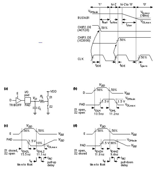
Figure 6.6 shows the timing of part of a bus transaction (a sequence of signals on a bus):
1.Initially CHIP2 drives BUSA.B1 high (CHIP2.D1 is '1' and CHIP2.OE is '1').
2.The buffer output enable on CHIP2 (CHIP2.OE) goes low, floating the bus. The bus will stay high because we have a bus keeper, BK1.
3.The buffer output enable on CHIP3 (CHIP3.OE) goes high and the buffer drives a low onto the bus (CHIP3.D1 is '0').
We wish to calculate the delays involved in driving the off-chip bus in Figure 6.6 . In order to find t float , we need to understand how Actel specifies the delays for its I/O cells. Figure 6.7 (a) shows the circuit used for measuring I/O delays for the ACT FPGAs. These measurements do not use the same trip points that are used to characterize the internal logic (Actel uses input and output trip points of 0.5 for
internal logic delays).
FIGURE 6.6 Three-state bus timing for Figure 6.5 . The on-chip delays, t 2OE and t 3OE , for the logic that generates
signals CHIP2.E1 and CHIP3.E1 are derived from the timing models described in Chapter 5 (the minimum
values for each chip would be the clock-to-Q delay times).
FIGURE 6.7 (a) The test circuit for characterizing the ACT 2 and ACT 3 I/O delay parameters. (b) Output buffer propagation delays from the data input to PAD (output enable, E, is high). (c) Three-state delay with D low. (d) Three-state delay with D high. Delays are shown for ACT 2 'Std' speed grade, worst-case commercial conditions ( R L = 1 k W , C L = 50 pF, V OHmin = 2.4 V, V OLmax = 0.5 V). (The Actel three-state buffer is named TRIBUFF, an input buffer INBUF, and the output buffer, OUTBUF.)
Notice in Figure 6.7 (a) that when the output enable E is '0' the output is three-stated ( high-impedance or hi-Z ). Different companies use different polarity and naming conventions for the output enable signal on a three-state buffer. To measure the buffer delay (measured from the change in the enable signal, E) Actel uses a resistor
load ( R L = 1 k W for ACT 2). The resistor pulls the buffer output high or low depending on whether we are measuring:
●t ENZL , when the output switches from hi-Z to '0'.
●t ENLZ , when the output switches from '0' to hi-Z.
●t ENZH , when the output switches from hi-Z to '1'.
●t ENHZ , when the output switches from '1' to hi-Z.
Other vendors specify the time to float a three-state output buffer directly (t fr and t ff in Figure 6.7 c and d). This delay time has different names (and definitions): disable time , time to begin hi-Z , or time to turn off .
Actel does not specify the time to float but, since R L C L = 50 ns, we know t RC = R L C L ln 0.9 or approximately 5.3 ns. Now we can estimate that
t fr = t ENLZ t RC = 11.1 5.3 = 5.8 ns, and tff = 9.4 5.3 = 4.1 ns,
and thus the Actel buffer can float the bus in t float = 4.1 ns ( Figure 6.6 ).
The Xilinx FPGA is responsible for the second part of the bus transaction. The time to make the buffer CHIP2.B1 active is t active . Once the buffer is active, the output transistors turn on, conducting a current I peak . The output voltage V O across the load
capacitance, C BUS , will slew or change at a steady rate, d V O / d t = I peak / C BUS ; thus t slew = C BUS D V O / I peak , where D V O is the change in output voltage.
Vendors do not always provide enough information to calculate t active and t slew separately, but we can usually estimate their sum. Xilinx specifies the time from the three-state input switching to the time the pad is active and valid for an XC3000-125 switching with a 50 pF load, to be t active = t TSON = 11 ns (fast option), and 27 ns (slew-rate limited option). 1 If we need to drive the bus in less than one clock cycle (30 ns), we will definitely need to use the fast option.
A supplement to the XC3000 timing data specifies the additional fall delay for switching large capacitive loads (above 50 pF) as R fall = 0.06 nspF 1 (falling) and R rise = 0.12 nspF 1 (rising) using the fast output option. 2 We can thus estimate that
I peak ª (5 V)/( 0.06 ¥ 103 sF 1 ) ª 84 mA (falling) and I peak ª (5 V)/(0.12 ¥ 10 3 sF 1 ) ª 42 mA (rising). Now we can calculate,
t slew = R fall ( C BUS 50 pF) = (90 pF 50 pF) (0.06 nspF 1 ) or 2.4 ns ,
for a total falling delay of 11 + 2.4 = 13.4 ns. The rising delay is slower at 11 + (40 pF)(0.12 nspF 1 ) or 15.8 ns. This leaves (30 15.8) ns, or about 14 ns worst-case, to generate the output enable signal CHIP2.OE (t 3OE in Figure 6.6 ) and still leave time t spare before the bus data is latched on the next clock edge. We can thus probably use a
XC3000 part for a 30 MHz bus transceiver, but only if we use the fast slew-rate option.
An aside: Our example looks a little like the PCI bus used on Pentium and PowerPC systems, but the bus transactions are simplified. PCI buses use a sustained three-state system ( s / t / s ). On the PCI bus an s / t / s driver must drive the bus high for at least one clock cycle before letting it float. A new driver may not start driving the bus until a clock edge after the previous driver floats it. After such a turnaround cycle a new driver will always find the bus parked high.
6.2.1 Supply Bounce
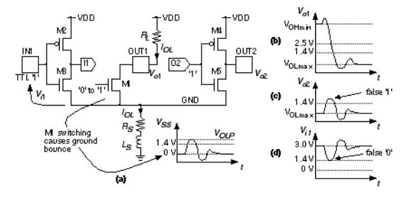
Figure 6.8 (a) shows an n -channel transistor, M1, that is part of an output buffer driving an output pad, OUT1; M2 and M3 form an inverter connected to an input pad, IN1; and M4 and M5 are part of another output buffer connected to an output pad, OUT2. As M1 sinks current pulling OUT1 low ( V o 1 in Figure 6.8 b), a substantial current I OL may flow in the resistance, R S , and inductance, L S , that are between the on-chip GND net and the off-chip, external ground connection.
FIGURE 6.8 Supply bounce. (a) As the pull-down device, M1, switches, it causes the GND net (value V SS ) to bounce. (b) The supply bounce is dependent on the output slew rate. (c) Ground bounce can cause other output buffers to generate a logic glitch. (d) Bounce can also cause errors on other inputs.
The voltage drop across R S and L S causes a spike (or transient) on the GND net, changing the value of V SS , leading to a problem known as supply bounce . The situation is illustrated in Figure 6.8 (a), with V SS bouncing to a maximum of V OLP . This ground bounce causes the voltage at the output, V o 2 , to bounce also. If the threshold of the gate that OUT2 is driving is a TTL level at 1.4 V, for example, a ground bounce of more than 1.4 V will cause a logic high glitch (a momentary transition from one logic level to the opposite logic level and back again).
Ground bounce may also cause problems at chip inputs. Suppose the inverter M2/M3
is set to have a TTL threshold of 1.4 V and the input, IN1, is at a fixed voltage equal to 3 V (a respectable logic high for bipolar TTL). In this case a ground bounce of greater than 1.6 V will cause the input, IN1, to see a logic low instead of a high and a glitch will be generated on the inverter output, I1. Supply bounce can also occur on the VDD net, but this is usually less severe because the pull-up transistors in an output buffer are usually weaker than the pull-down transistors. The risk of generating a glitch is also greater at the low logic level for TTL-threshold inputs and TTL-level outputs because the low-level noise margins are smaller than the high-level noise margins in TTL.
Sixteen SSOs, with each output driving 150 pF on a bus, can generate a ground bounce of 1.5 V or more. We cannot simulate this problem easily with FPGAs because we are not normally given the characteristics of the output devices. As a rule of thumb we wish to keep ground bounce below 1 V. To help do this we can limit the maximum number of SSOs, and we can limit the number of I/O buffers that share GND and VDD pads.
To further reduce the problem, FPGAs now provide options to limit the current flowing in the output buffers, reducing the slew rate and slowing them down. Some FPGAs also have quiet I/O circuits that sense when the input to an output buffer changes. The quiet I/O then starts to change the output using small transistors; shortly afterwards the large output transistors drop-in. As the output approaches its final value, the large transistors kick-out, reducing the supply bounce.
6.2.2 Transmission Lines
Most of the problems with driving large capacitive loads at high speed occur on a bus, and in this case we may have to consider the bus as a transmission line. Figure 6.9 (a) shows how a transmission line appears to a driver, D1, and receiver, R1, as a constant impedance, the characteristic impedance of the line, Z 0 . For a typical PCB trace, Z 0 is between 50 W and 100 W .
FIGURE 6.9 Transmission lines. (a) A printed-circuit board (PCB) trace is a transmission (TX) line. (b) A driver launches an incident wave, which is reflected at the end of the line. (c) A connection starts to look like a transmission line when the signal rise time is about equal to twice the line delay (2 t f ).
The voltages on a transmission line are determined by the value of the driver source resistance, R 0 , and the way that we terminate the end of the transmission line. In Figure 6.9 (a) the termination is just the capacitance of the receiver, C in . As the driver switches between 5 V and 0 V, it launches a voltage wave down the line, as shown in Figure 6.9 (b). The wave will be Z 0 / ( R 0 + Z 0 ) times 5 V in magnitude, so that if R 0 is equal to Z 0 , the wave will be 2.5 V.
Notice that it does not matter what is at the far end of the line. The bus driver sees only Z 0 and not C in . Imagine the transmission line as a tunnel; all the bus driver can see at the entrance is a little way into the tunnel it could be 500 m or 5 km long. To find out, we have to go with the wave to the end, turn around, come back, and tell the bus driver. The final result will be the same whether the transmission line is there or not, but with a transmission line it takes a little longer for the voltages and currents to settle down. This is rather like the difference between having a conversation by telephone or by post.
The propagation delay (or time of flight), t f , for a typical PCB trace is approximately 1 ns for every 15 cm of trace (the signal velocity is about one-half the speed of light). A voltage wave launched on a transmission line takes a time t f to get to the end of the line, where it finds the load capacitance, C in . Since no current can flow at this point, there must be a reflection that exactly cancels the incident wave so that the voltage at the input to the receiver, at V 2 , becomes exactly zero at time t f . The reflected wave travels back down the line and finally causes the voltage at the output of the driver, at V 1 , to be exactly zero at time 2 t f . In practice the nonidealities of the driver and the line cause the waves to have finite rise times. We start to see transmission line behavior if the rise time of the driver is less than 2 t f , as shown in Figure 6.9 (c).
There are several ways to terminate a transmission line. Figure 6.10 illustrates the following methods:
●Open-circuit or capacitive termination. The bus termination is the input capacitance of the receivers (usually less than 20 pF). The PCI bus uses this method.
●Parallel resistive termination. This requires substantial DC current (5 V / 100 W = 50 mA for a 100 W line). It is used by bipolar logic, for example
emitter-coupled logic (ECL), where we typically do not care how much power we use.
●Thévenin termination. Connecting 300 W in parallel with 150 W across a 5 V supply is equivalent to a 100 W termination connected to a 1.6 V source. This reduces the DC current drain on the drivers but adds a resistance directly across the supply.
●Series termination at the source. Adding a resistor in series with the driver so that the sum of the driver source resistance (which is usually 50 W or even less) and the termination resistor matches the line impedance (usually around 100 W ). The disadvantage is that it generates reflections that may be close to the switching threshold.
●Parallel termination with a voltage bias. This is awkward because it requires a
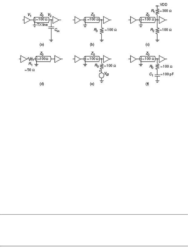
third supply and is normally used only for a specialized high-speed bus.
●Parallel termination with a series capacitance. This removes the requirement for DC current but introduces other problems.
FIGURE 6.10 Transmission line termination. (a) Open-circuit or capacitive termination. (b) Parallel resistive termination. (c) Thévenin termination.
(d) Series termination at the source. (e) Parallel termination using a voltage bias. (f) Parallel termination with a series capacitor.
Until recently most bus protocols required strong bipolar or BiCMOS output buffers capable of driving all the way between logic levels. The PCI standard uses weaker CMOS drivers that rely on reflection from the end of the bus to allow the intermediate receivers to see the full logic value. Many FPGA vendors now offer complete PCI functions that the ASIC designer can drop in to an FPGA [PCI, 1995].
An alternative to using a transmission line that operates across the full swing of the supply voltage is to use current-mode signaling or differential signals with low-voltage swings. These and other techniques are used in specialized bus structures and in high-speed DRAM. Examples are Rambus, and Gunning transistor logic ( GTL ). These are analog rather than digital circuits, but ASIC methods apply if the interface circuits are available as cells, hiding some of the complexity from the designer. For example, Rambus offers a Rambus access cell ( RAC ) for standard-cell design (but not yet for an FPGA). Directions to more information on these topics are in the bibliography at the end of this chapter.
1.1994 data book, p. 2-159.
2.Application Note XAPP 024.000, Additional XC3000 Data, 1994 data book p. 8-15.