

5.6 Problems
* = Difficult, ** = Very difficult, *** = Extremely difficult
5.1 (Using the ACT 1 Logic Module, 30 min.) Consider the Actel ACT 1 Logic Module shown in Figure 5.1 . Show how to implement: (a) a three-input NOR gate, (b) a three-input majority function gate, (c) a 2:1 MUX, (d) a half adder,
(e) a three-input XOR gate, and (f) a four-input MUX.
5.2(Worst-case and best-case timing, 10 min.) Seasoned digital CMOS designers do not worry too much when their designs stop working when they get too hot or when they reduce the supply voltage, but an ASIC that stops working either when increasing the supply voltage above normal or when it gets cold causes panic.
Why?
5.3(Typical to worst-case variation, 10 min.) The 1994 Actel data book (p. 1-5) remarks that: the total derating factor from typical to worst-case for a standard ACT 1 array is only 1.19:1, compared to 2:1 for a masked gate array.
●a. Can you explain why this is when the basic ACT 1 CMOS process is identical to a CMOS process for masked gate arrays?
●b. There is a price to pay for the reduced spread in timing delays from typical to worst-case in an ACT 1 array. What is this disadvantage of the ACT 1 array over a masked gate array?
5.4(ACT 2/3 sequential element, 30 min.). Show how the Actel ACT 2 and ACT 3 sequential element of Figure 5.4 (used in the S-Module) can be wired to
implement:
●a. a positive-edge triggered flip-flop with clear,
●b. a negative-edge triggered flip-flop with clear,
●c. a transparent-high latch,
●d. a transparent-low latch, and
●e. how it can be made totally transparent.
5.5(*ACT 1 logic functions, 40 min.+)
●a. How many different combinational functions of four logic variables are there?
●b. of n variables? Hint: Consider the truth table.
●c. The ACT 1 module can implement 213 of the 256 functions with three variables. How many of the 43 three-input functions that it cannot
implement can you find?
●d. (harder) Show that if you have access to both the true and complement form of the input variables you can implement all 256 logic functions of three variables with the ACT 1 Logic Module.
5.6(Actel and Xilinx, 10 min.) The Actel Logic Modules (ACT 1, ACT 2, and ACT 3) have eight inputs and can implement most three-input logic functions and a few logic functions with four input variables. In contrast, the Xilinx XC5200 CLB, for example, has only four inputs but can implement all logic functions with four or fewer variables. Why would Actel choose these logic cell designs and how can they be competitive with the Xilinx FPGA (which they are)?
5.7(Actel address decoders, 10 min.) The maximum number of inputs that the ACT 1 Logic Module can handle is four. The ACT 2/ACT 3 C-module increases this to five.
●a. How many ACT 1 Logic Modules do you need to implement a 32-bit wide address decoder (a 32-input AND gate)?
●b. How many ACT 2/ACT 3 C-modules do you need?
5.8(Altera shared logic expanders, 30 min.) Consider an Altera MAX 5000 logic array with three product-term lines. You cannot directly implement the function Z = A · B · C + A · B' · C' + A' · B · C' + A' · B' · C with a programmable array logic macrocell that has only three product-term lines, since Z has four product terms.
●a. How many Boolean functions of three variables are there that cannot be implemented with a programmable array logic macrocell that has only three product terms? Hint: Use a Karnaugh map to consider how many Boolean functions of three variables have more than three product terms in their sum-of-products representation.
●b. Show how to use shared logic expanders that feed terms back into the product-term array to implement the function Z using a macrocell with three product terms.
●c. How many shared expander lines do you need to add to be able to implement all the Boolean functions of three variables?
●d. What is the largest number of product terms that you need to implement a Boolean function with n variables?
5.9(Splitting the XC3000 CLB, 20 min.) In Section 5.2.1 we noted You can split
the (XC3000) 32-bit LUT in half, using one of the seven input variables to switch between the F and G outputs. This technique can implement some functions of six and seven variables.
●a. Show which functions of six and seven variables can, and
●b. which functions cannot, be implemented using this method.
5.10(Programmable inversion, 20 min.) Section 5.4 described how the Altera
MAX series logic cells can use programmable inversion to reduce the number of product terms needed to implement a function. Give another example of a function of four variables that requires four product terms. Is there a way to tell how many product terms a function may require?
5.11 (Table look-up mapping, 20 min.) Consider a four-input LUT (used in the CLB in the Xilinx XC2000, the first generation of Xilinx FPGAs, and in the XC5200 LE). This CLB can implement any Boolean function of four variables. Consider the function
Z = (A · (B + C)) + (B · D) + (E · F · G · H · I) .(5.27)
We can use four CLBs to implement Z as follows:
CLB1: Z = Z1 + (B · D) + Z3 ,
CLB2: Z1 = A · (B + C) ,
CLB3: Z3 = E · F · G · Z5 ,
CLB4: Z5 = H · I .(5.28)
What is the length of the critical path? Find a better assignment in terms of area and critical path.
5.12 (Multiplexer mapping, 10 min.) Consider the function:
F = (A · B) + (B' · C) + D .(5.29)
Use Shannon s expansion theorem to expand F wrt B:
F = B · F1 + B' · F2 .(5.30)
In other words express F in terms of B, B', F1, and F2 ( Hint: F1 is a function of A and D only, F2 is a function of C and D only). Now expand F1 wrt A, and F2 wrt C. Using your answer, implement F using a single ACT 1 Logic Module.
5.13(*Xilinx hazards, 10 min.) Explain why the outputs of the Xilinx CLBs are hazard-free for input changes in only one variable. Is this important?
5.14(**Actel S-Modules, 10 min.) Notice that CLR is tied to the input corresponding to B0 of the C-module in the ACT 2 S-Module but the CLR input is separate from the B0 input in the ACT 3 version. Why?
5.15(**Timing estimates, 60 min.) Using data book values for an FPGA architecture that you choose, and explaining your calculations carefully, estimate the (worst-case commercial) delay for the following functions: (a) 16-bit address decoder, (b) 8-bit ripple-carry adder, (c) 8-bit ripple-carry counter. Give your answers in terms of the data book symbols, and using actual parameters, for a speed grade that you specify, give an example calculation with the delay in ns.
5.16(Actel logic. 30 min.) Table 5.10 shows how to use the Actel ACT 1 Logic
Module to implement some of the 16 functions of two input variables. Complete this table.
TABLE 5.10 Boolean functions using the ACT 1 Logic Module (Problem 5.16).
Function, F |
F = |
Canonical form |
Minterms M1 |
|
M2 |
OR1 |
||
|
|
|
|
|
A0 A1 SA B0 B1 SB S0 S1 |
|||
1 |
0 |
0 |
0 |
|
0 |
0 |
0 |
|
2 |
AND(A, B) |
A · B A · B |
3 |
0 |
B |
A |
|
|
3 |
AND1-1(A, B) |
A · |
A · B' |
2 |
A |
0 |
B |
|
B' |
|
|||||||
|
|
|
|
|
|
|
|
|
4 |
NOR(A, B) |
A + |
A' · B' |
0 |
|
|
|
|
B |
|
|
|
|
||||
|
|
|
|
|
|
|
|
|
5 |
NOR1-1(A, B) |
A + |
A' · B |
1 |
B |
0 |
A |
|
B' |
|
|||||||
|
|
|
|
|
|
|
|
|
6 |
A |
A |
A · B' + A · B |
2, 3 |
0 A |
1 |
|
|
7 |
B |
B |
A' · B + A · B |
1, 3 |
0 B |
1 |
|
|
8 |
NOT(A) |
A' |
A' · B' + A' · B |
0, 1 |
0 |
1 |
A |
|
9 |
NOT(B) |
B' |
A' · B' + A · B' |
0, 2 |
0 |
1 |
B |
|
10 EXOR(A, B) |
A • |
A' · B + A · B' |
1, 2 |
|
|
|
|
|
B |
|
|
|
|
||||
|
|
|
|
|
|
|
|
|
11 EXNOR(A, B) |
(A • |
A' · B' + A · B |
0, 3 |
|
|
|
|
|
B) |
|
|
|
|
||||
|
|
|
|
|
|
|
|
|
12 OR(A, B) |
A + |
A' · B + A · B' + |
1, 2, 3 |
B |
1 |
A |
|
|
|
|
B |
A · B |
|
|
|
|
|
13 OR1-1(A, B) |
A + |
A' · B' + A · B' |
0, 2, 3 |
|
|
|
|
|
B' |
+ A · B |
|
|
|
|
|||
|
|
|
|
|
|
|
||
14 NAND(A, B) |
(A · |
A' · B' + A' · B |
0, 1, 2 |
|
|
|
|
|
B)' |
+ A · B' |
|
|
|
|
|||
|
|
|
|
|
|
|
||
|
|
(A · |
A' · B' + A' · B |
|
|
|
|
|
15 NAND1-1(A, B) B')' |
+ A · B |
0, 1, 3 |
|
|
|
|
||
16 1 |
1 |
A' · B' + A' · B |
0, 1, 2, 3 1 |
1 |
1 |
|
||
+ A · B' + A · B |
|
|||||||
5.17(ACT 1 module implementation, 120 min.)
●a. Show that the circuit shown in Figure 5.17 , with buffered inputs and outputs, is equivalent to the one shown in Figure 5.1 .
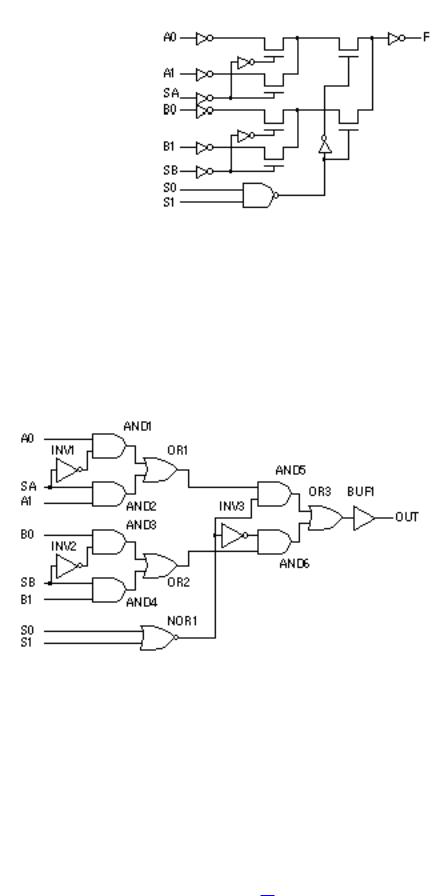
FIGURE 5.17 An alternative implementation of the ACT 1 Logic Module shown in Figure 5.1 (Problem 5.17).
●b. Show that the circuit for the ACT 1 Logic Module shown in Figure 5.18 is also the same.
●c. Convert the circuit of Figure 5.18 to one that uses more efficient CMOS gates: inverters, AOI, and NAND gates.
●d. (harder) Assume that the ACT 1 Logic Module has the equivalent of a 2X drive and the logic ratio is close to one. Compare your answer to part c against Figure 5.17 in terms of logical efficiency and logical area.
FIGURE 5.18 A schematic equivalent of the Actel ACT 1 Logic Module (Problem 5.17).
5.18 (**Xilinx CLB analysis, 60 min.) Table 5.11 shows some information derived from a die photo in the AT&T ATT3000 series data book that shows the eight by eight CLB matrix on an ATT3020 (equivalent to a XC3020) clearly. By measuring the die size in the photo and knowing the actual die size we can calculate the size of a CLB matrix element ( ME ) that includes a single XC3000 CLB as approximately 277 mil 2 . The ME includes interconnect, SRAM, programming, and other resources as well as a CLB.
TABLE 5.11 ATT3020 die information (Problem 5.18). 1
Parameter |
Data book Die photo |
Calculated |
3020 die width |
183.5 mil 4.1 cm |
|

3020 die height |
219.3 mil |
4.9 cm |
|
3000 ME width |
0.325 cm |
14.55 mil = 370 m m |
|
3000 ME height |
0.425 cm |
19.02 mil = 483 m m |
|
3000 ME area |
|
|
277 mil 2 |
3020 pad pitch |
|
1.6 mm / pad 7.21 mil / pad |
|
●a. The minimum feature size in the AT&T Holmdel twin-tub V process used for the ATT3000 family is 0.9 m m. Using a value of l = 0.45 m m, calculate the Xilinx XC3000 ME size in l 2 .
●b. Estimate, explaining your assumptions, the area of the XC4000 ME, and the XC5200 ME (both in l 2 ).
●c. Table 5.12 shows the ATT3000 die information. Using a value of 277 mil 2 for the ATT/XC3000 ME area, complete this table.
TABLE 5.12 ATT3000 die information (Problem 5.18). 2 |
|
||||||||
|
|
|
|
|
|
|
|
|
|
|
Die height Die width |
|
Die |
|
ME |
ME |
|||
Die |
Die area mil 2 area |
CLBs area |
area |
||||||
mil |
mil |
||||||||
|
|
cm2 |
|
mil 2 |
cm2 |
||||
|
|
|
|
|
|||||
3020 |
219.3 |
183.5 |
40,242 |
0.26 |
8 ¥ 8 |
|
|
|
|
3030 |
259.8 |
215.0 |
55,857 |
0.36 |
10 ¥ 10 |
|
|
||
3042 |
295.3 |
242.5 |
71,610 |
0.46 |
12 ¥ 12 |
|
|
||
3064 |
270.9 |
366.5 |
99,285 |
0.64 |
16 ¥ 14 |
|
|
||
3090 |
437.0 |
299.2 |
130,750 |
0.84 |
16 ¥ 20 |
|
|
||
1.Data from AT&T data book, July 1992, p. 3-76, MN92-024FPGA
2.Data from AT&T data book, July 1992, p. 3-75, MN92-024FPGA. 1 mil 2 = 106 in 2 = 2.54 2 ¥ 10 6 cm 2 = 6.452 ¥ 10 6 cm 2